
We invite all engineers, researchers, entrepreneurs, inventors, and end users active in the development or manufacturing or applications of perovskite technology to join this fantastic one-day event.
This one-day curated event focuses on all aspects of perovskite technologies, from material development to processing to applications in lighting, displays, photovoltaics, and beyond.
This event is co-organised by TechBlick and Perovskite-Info.com.
This event will also feature a parallel track dedicated to innovations in (a) additive, printed, hybrid and sustainable electronics and (2) MicroLED + AR/VR display technologies.
Full Agenda
Berlin Time
Track 1
Sumitomo Metal Mining

joint
Sumitomo Metal Mining
1:30 PM
Development of nano copper powder with oxidation-resistant and air stable copper based MOD Paste for Printed Electronics
Abstract

Kentaro Nakatsuji
We develop unique conductive materials for an energy-smart, sustainable world using our core technique. This talk introduces newly developed items, which are oxidation-resistant nano copper powder and MOD (metal-organic decomposition) paste for printed electronics. Our fine copper powder shows uniform size, strong oxidation resistance, and dense sintering near 200℃.
Also, MOD paste consists of MOD ink and its Cu powder to obtain film thickness—from thin lines to thick buses, over 3× typical nano inks—while keeping copper-like conductivity.
During curing, a protective layer forms on Cu, enabling reliable, low-resistance paths for high-current and large-area devices and compact modules. We aim to bring affordable, scalable copper printing to mainstream manufacturing.
Development of nano copper powder with oxidation-resistant and air stable copper based MOD Paste for Printed Electronics
1:30 PM
We develop unique conductive materials for an energy-smart, sustainable world using our core technique. This talk introduces newly developed items, which are oxidation-resistant nano copper powder and MOD (metal-organic decomposition) paste for printed electronics. Our fine copper powder shows uniform size, strong oxidation resistance, and dense sintering near 200℃.
Also, MOD paste consists of MOD ink and its Cu powder to obtain film thickness—from thin lines to thick buses, over 3× typical nano inks—while keeping copper-like conductivity.
During curing, a protective layer forms on Cu, enabling reliable, low-resistance paths for high-current and large-area devices and compact modules. We aim to bring affordable, scalable copper printing to mainstream manufacturing.
Arkema Piezotech

joint
Arkema Piezotech
1:45 pm
Electroactive Polymers: Bringing Sensitivity to Printed Electronics
Abstract

Mickael Pruvost
Research And Development Engineer
Printed electronics are evolving fast, and electroactive polymers are paving the way for a new generation of devices that don’t just perform—they feel. Available as powders, inks, and films, these materials combine the versatility of polymers with piezoelectric functionality, enabling electronics that respond to touch, vibration, and impact.
With their printability, flexibility, and lightweight design, electroactive polymers make it possible to create highly sensitive sensors across a wide frequency range. They are already opening opportunities in automotive (safer human–machine interfaces), energy (structural health monitoring of hydrogen tanks and batteries), healthcare (vital signs monitoring), acoustics (musical pickups), and sports (impact detection).
This talk will demystify piezoelectric polymers and show how they can be implemented in real applications. Attendees will discover why these materials are an essential platform for innovation in tomorrow’s smart and sustainable electronics.
Electroactive Polymers: Bringing Sensitivity to Printed Electronics
1:45 pm
Printed electronics are evolving fast, and electroactive polymers are paving the way for a new generation of devices that don’t just perform—they feel. Available as powders, inks, and films, these materials combine the versatility of polymers with piezoelectric functionality, enabling electronics that respond to touch, vibration, and impact.
With their printability, flexibility, and lightweight design, electroactive polymers make it possible to create highly sensitive sensors across a wide frequency range. They are already opening opportunities in automotive (safer human–machine interfaces), energy (structural health monitoring of hydrogen tanks and batteries), healthcare (vital signs monitoring), acoustics (musical pickups), and sports (impact detection).
This talk will demystify piezoelectric polymers and show how they can be implemented in real applications. Attendees will discover why these materials are an essential platform for innovation in tomorrow’s smart and sustainable electronics.
NanoSen GmbH

joint
NanoSen GmbH
2:00 pm
NanoSen PNC Force Sensors for Printed and Hybrid Electronics
Abstract

Joseph Stephens
Grndungsmitglied
This 10-minute tech talk introduces NanoSen PNC Force Sensors, a breakthrough in printed and hybrid electronics. Leveraging our specially developed piezoresitive and piezocapacitive polymer nanocomposite (PNC) material, this sensor material can be seamlessly integrated with flexible substrates, enabling robust, sensitive, and adaptable force measurements via impedance readout electronics. A single 20mm sensor can measure 0.01 newton - 150 newton and withstand 20 megapascals of pressure before the material is damaged. We have also tested the robustness with 20 million cycles á 200 newtons of force, without experiencing material degredation.
The talk will highlight their durability, flexibility for applications like wearables and robotics, and high sensitivity for precise force detection in medical and consumer devices. Attendees will explore real-world use cases with printed electrodes made from different substrates and configurations to show the future potential of this innovative technology.
NanoSen PNC Force Sensors for Printed and Hybrid Electronics
2:00 pm
This 10-minute tech talk introduces NanoSen PNC Force Sensors, a breakthrough in printed and hybrid electronics. Leveraging our specially developed piezoresitive and piezocapacitive polymer nanocomposite (PNC) material, this sensor material can be seamlessly integrated with flexible substrates, enabling robust, sensitive, and adaptable force measurements via impedance readout electronics. A single 20mm sensor can measure 0.01 newton - 150 newton and withstand 20 megapascals of pressure before the material is damaged. We have also tested the robustness with 20 million cycles á 200 newtons of force, without experiencing material degredation.
The talk will highlight their durability, flexibility for applications like wearables and robotics, and high sensitivity for precise force detection in medical and consumer devices. Attendees will explore real-world use cases with printed electrodes made from different substrates and configurations to show the future potential of this innovative technology.
Integrated Graphene (iGii)

joint
Integrated Graphene (iGii)
2:15 pm
Revolutionsing Functional Devices : A Scalable 3D Carbon Nanomaterial Platform for Next-Generation Applications
Abstract

Michelle Ntola
Principle Development Scientist
Three-dimensional (3D) carbon nanomaterials are transforming the landscape of functional materials, unlocking new possibilities in sectors ranging from diagnostics and energy storage to smart sensing and thermal management. Their unique three-dimensional architecture and tuneable properties enable the development of high-performance, cost-effective, and sustainable solutions that are compatible with existing technology systems.
At the forefront of this innovation is Gii, our proprietary 3D carbon material platform, engineered for seamless integration across diverse application systems. This presentation will showcase recent breakthroughs in Gii’s deployment across a spectrum of use cases, including:
Electrochemical sensing: for real-time diagnostics and environmental monitoring
Printed batteries: for flexible, lightweight energy storage, IoT, wearables, and digital health applications
Pressure and strain sensors: for wearable devices and occupancy monitoring
Microheaters: for localised thermal control in biosensors, microreactors and other compact systems
Catalytic platforms: for energy and chemical processing applications
Gii™ not only addresses the limitations of conventional material system, such as durability, high cost, and limited scalability, but also delivers superior performance metrics:
High surface area: specific electroactive surface area of 3 – 4 times the geometric area
Electrical conductivity: 5 – 10 Ω/square at room temperature
Functionalisation: can be functionalised with metal oxides, bioreceptors, ion-selective membranes
Thermal conductivity: 3.8 W/mK and temperature coefficient of resistance of 0.0013/°C to -0.000488/°C)
Chemical stability: compatible with most organic and aqueous solutions, stable in solutions from pH 0 – pH 10
Anti-fouling: no performance loss after 30 min exposure in whole milk
Additionally, Gii is manufactured using roll-to-roll and roll-to-sheet compatible, low-temperature fabrication processes, enabling scalable production capable of producing 80 million parts per year per machine. This positions Gii as a commercially viable solution for industries seeking to accelerate product innovation without compromising on performance, cost or sustainability.
Join our presentation to explore how Gi is redefining advanced materials for next-generation devices and how your industry can benefit from its potential.
Revolutionsing Functional Devices : A Scalable 3D Carbon Nanomaterial Platform for Next-Generation Applications
2:15 pm
Three-dimensional (3D) carbon nanomaterials are transforming the landscape of functional materials, unlocking new possibilities in sectors ranging from diagnostics and energy storage to smart sensing and thermal management. Their unique three-dimensional architecture and tuneable properties enable the development of high-performance, cost-effective, and sustainable solutions that are compatible with existing technology systems.
At the forefront of this innovation is Gii, our proprietary 3D carbon material platform, engineered for seamless integration across diverse application systems. This presentation will showcase recent breakthroughs in Gii’s deployment across a spectrum of use cases, including:
Electrochemical sensing: for real-time diagnostics and environmental monitoring
Printed batteries: for flexible, lightweight energy storage, IoT, wearables, and digital health applications
Pressure and strain sensors: for wearable devices and occupancy monitoring
Microheaters: for localised thermal control in biosensors, microreactors and other compact systems
Catalytic platforms: for energy and chemical processing applications
Gii™ not only addresses the limitations of conventional material system, such as durability, high cost, and limited scalability, but also delivers superior performance metrics:
High surface area: specific electroactive surface area of 3 – 4 times the geometric area
Electrical conductivity: 5 – 10 Ω/square at room temperature
Functionalisation: can be functionalised with metal oxides, bioreceptors, ion-selective membranes
Thermal conductivity: 3.8 W/mK and temperature coefficient of resistance of 0.0013/°C to -0.000488/°C)
Chemical stability: compatible with most organic and aqueous solutions, stable in solutions from pH 0 – pH 10
Anti-fouling: no performance loss after 30 min exposure in whole milk
Additionally, Gii is manufactured using roll-to-roll and roll-to-sheet compatible, low-temperature fabrication processes, enabling scalable production capable of producing 80 million parts per year per machine. This positions Gii as a commercially viable solution for industries seeking to accelerate product innovation without compromising on performance, cost or sustainability.
Join our presentation to explore how Gi is redefining advanced materials for next-generation devices and how your industry can benefit from its potential.
Exhibition & Refreshment Break

joint
Exhibition & Refreshment Break
2:30 PM
Exhibition & Refreshment Break
Abstract
Exhibition & Refreshment Break
2:30 PM
Alqio


Fabien Resweber
Armor Smart Films, an ARMOR Group company is a trusted industrial partner, supporting clients from design to large-scale production of functionalized surfaces.
With advanced capabilities in coating, printing, and formulation, Armor Smart helps accelerate innovation and market entry.
A key focus lies in electroactive technologies using P(VDF-TrFE) copolymers, known for their excellent piezoelectric properties.
These materials enable the development of next-generation sensors, haptic interfaces, heating surfaces, and medical instrumentation—combining flexibility, efficiency, and seamless integration.
Empowering Scalable Innovation in Functional Surfaces
3:00 pm
Armor Smart Films, an ARMOR Group company is a trusted industrial partner, supporting clients from design to large-scale production of functionalized surfaces.
With advanced capabilities in coating, printing, and formulation, Armor Smart helps accelerate innovation and market entry.
A key focus lies in electroactive technologies using P(VDF-TrFE) copolymers, known for their excellent piezoelectric properties.
These materials enable the development of next-generation sensors, haptic interfaces, heating surfaces, and medical instrumentation—combining flexibility, efficiency, and seamless integration.
BLACKLEAF


Michael Friess
Sales director
Blackleaf produces graphene-based heating inks.
Thanks to an innovative and sustainable graphene production process, combined with deep expertise in chemical formulation, we offer our clients comprehensive solutions and a diversified portfolio of graphene-based heatable inks.
Our heating inks are used to bring heat onto surfaces through two complementary methods: flexible heating foils and heating coatings.
Graphene-based Electric Heating: How Graphene Films Are Reinventing Surface Heating in the Industry
3:15 pm
Blackleaf produces graphene-based heating inks.
Thanks to an innovative and sustainable graphene production process, combined with deep expertise in chemical formulation, we offer our clients comprehensive solutions and a diversified portfolio of graphene-based heatable inks.
Our heating inks are used to bring heat onto surfaces through two complementary methods: flexible heating foils and heating coatings.
Komori America Corporation


Reza Kazemi
Business Development Manager
Using gravure offset technology under development, we have created an advanced micro-printing process capable of producing fine patterns with high positional accuracy (±5 µm, 3σ) and feature sizes down to 5 µm. This approach enables precise alignment for multilayer printing, allowing controlled thickness build-up without defects. It is optimized for micro-solder and copper paste deposition, supporting next-generation applications such as high-density surface-mount components, micro-bumps, and micro-LED assembly. By eliminating plating processes, it offers an eco-friendly alternative while ensuring high reliability and strong resistance to migration. Ongoing developments include nano-copper pastes with excellent conductivity and fine-line capability, expanding the potential for dense, high-performance interconnects in advanced packaging and printed electronics.
Advancing Micro-Printing: High-Precision Gravure Offset for Next-Generation Electronics
3:30 pm
Using gravure offset technology under development, we have created an advanced micro-printing process capable of producing fine patterns with high positional accuracy (±5 µm, 3σ) and feature sizes down to 5 µm. This approach enables precise alignment for multilayer printing, allowing controlled thickness build-up without defects. It is optimized for micro-solder and copper paste deposition, supporting next-generation applications such as high-density surface-mount components, micro-bumps, and micro-LED assembly. By eliminating plating processes, it offers an eco-friendly alternative while ensuring high reliability and strong resistance to migration. Ongoing developments include nano-copper pastes with excellent conductivity and fine-line capability, expanding the potential for dense, high-performance interconnects in advanced packaging and printed electronics.
Policrom Screens Spa


Giorgio Bisutti
President
Printing electrical circuits on TPU (thermoplastic polyurethane) substrates opens the door to a wide range of applications in wearable and flexible electronics. Typically, though not exclusively, these circuits are transferred onto woven or nonwoven textiles, enabling functions such as signal transmission, stretch monitoring, heat transfer, and more.
The Challenges
Despite its potential, screen printing conductive and carbon inks on TPU presents significant difficulties:
• Printing process: TPU sheets often stick to the mesh or lift off the platen, disrupting the process.
• Curing phase: Exposure to the curing temperature compromises the flatness and dimensional accuracy of TPU, causing a total loss of image registration.
• Transfer to textile: During the final bonding step, the heat required to adhere the printed circuit to the textile softens the TPU, damaging the tracks and reducing conductivity.
These issues frequently lead to high scrap rates and, in many cases, make it impossible to produce a reliable circuit.
Our Solution:
To overcome these challenges, we have developed a dedicated product line and an application process that eliminate the critical issues of TPU printing and enable the production of multi-layer circuits.
This innovative material combines:
• A multilayer TPU film
• A heat-stabilized PET film
The lamination of these two components ensures perfect flatness and thermal stability, both essential for consistent and accurate printing results.
When used together with our encapsulant product, it becomes part of a system specifically designed for multi-layer electronic circuits, ensuring durability, reliability, and improved conductivity
Innovation in TPU
3:45 pm
Printing electrical circuits on TPU (thermoplastic polyurethane) substrates opens the door to a wide range of applications in wearable and flexible electronics. Typically, though not exclusively, these circuits are transferred onto woven or nonwoven textiles, enabling functions such as signal transmission, stretch monitoring, heat transfer, and more.
The Challenges
Despite its potential, screen printing conductive and carbon inks on TPU presents significant difficulties:
• Printing process: TPU sheets often stick to the mesh or lift off the platen, disrupting the process.
• Curing phase: Exposure to the curing temperature compromises the flatness and dimensional accuracy of TPU, causing a total loss of image registration.
• Transfer to textile: During the final bonding step, the heat required to adhere the printed circuit to the textile softens the TPU, damaging the tracks and reducing conductivity.
These issues frequently lead to high scrap rates and, in many cases, make it impossible to produce a reliable circuit.
Our Solution:
To overcome these challenges, we have developed a dedicated product line and an application process that eliminate the critical issues of TPU printing and enable the production of multi-layer circuits.
This innovative material combines:
• A multilayer TPU film
• A heat-stabilized PET film
The lamination of these two components ensures perfect flatness and thermal stability, both essential for consistent and accurate printing results.
When used together with our encapsulant product, it becomes part of a system specifically designed for multi-layer electronic circuits, ensuring durability, reliability, and improved conductivity
Nagase ChemteX America, LLC.


Alan Brown
Visible
Screen printed conductive inks offer a cost-effective and versatile method for creating biosensors. By depositing these inks onto flexible substrates, researchers can fabricate conformable and lightweight sensing platforms. This technique is particularly valuable for developing point-of-care diagnostics and wearable devices for continuous health monitoring, as it allows for the rapid and scalable production of sensors with high sensitivity and specificity.
Conductive Inks for Medical/ Wearable Electronics
4:00 pm
Screen printed conductive inks offer a cost-effective and versatile method for creating biosensors. By depositing these inks onto flexible substrates, researchers can fabricate conformable and lightweight sensing platforms. This technique is particularly valuable for developing point-of-care diagnostics and wearable devices for continuous health monitoring, as it allows for the rapid and scalable production of sensors with high sensitivity and specificity.
Exhibition & Refreshment Break
joint
Exhibition & Refreshment Break
4:15 pm
Exhibition & Refreshment Break
Abstract
Exhibition & Refreshment Break
4:15 pm
DELO Industrial Adhesives

Sven Hujo
Reliability of adhesives for MiniLED/MicroLED interconnects
This study investigates the long-term reliability of directional conductive adhesives (DCA) for electrical and mechanical interconnects in MiniLED and MicroLED applications. Building on a previous feasibility study from 2024, the adhesive bonds are subjected to extensive temperature and moisture resistance testing.
Key points:
- Evaluation of three adhesives for semiconductor mass production
- Performance of "light-on" tests, measurement of die-shear strength and U-I characteristics
- Tests under different conditions: Initial, after 500 h at 85°C/85% RH and after 500 h at 120°C
- Analysis of electrical and mechanical properties before and after storage
The results show excellent stability of the adhesive bonds, especially at 120°C storage.
This study represents an important step towards the commercialization of MiniLED and MicroLED applications and positions adhesive technology as a key element for future scalability and cost efficiency in production
Investigation of Electrically Conductive Adhesives for Miniaturized SMD Components
4:45 pm
Reliability of adhesives for MiniLED/MicroLED interconnects
This study investigates the long-term reliability of directional conductive adhesives (DCA) for electrical and mechanical interconnects in MiniLED and MicroLED applications. Building on a previous feasibility study from 2024, the adhesive bonds are subjected to extensive temperature and moisture resistance testing.
Key points:
- Evaluation of three adhesives for semiconductor mass production
- Performance of "light-on" tests, measurement of die-shear strength and U-I characteristics
- Tests under different conditions: Initial, after 500 h at 85°C/85% RH and after 500 h at 120°C
- Analysis of electrical and mechanical properties before and after storage
The results show excellent stability of the adhesive bonds, especially at 120°C storage.
This study represents an important step towards the commercialization of MiniLED and MicroLED applications and positions adhesive technology as a key element for future scalability and cost efficiency in production
Heraeus Electronics


Jessica Waite
The performance of silver conductive inks is critically influenced by the parameters of the drying process, particularly temperature and time. This presentation explores how these factors affect the electrical conductivity, adhesion, and overall functionality of printed silver traces. Through a series of controlled experiments, we examine the interplay between drying temperature and duration, highlighting optimal conditions for achieving low resistivity and robust film formation without compromising substrate compatibility.
How altering drying properties affects conductive ink performance
5:00 pm
The performance of silver conductive inks is critically influenced by the parameters of the drying process, particularly temperature and time. This presentation explores how these factors affect the electrical conductivity, adhesion, and overall functionality of printed silver traces. Through a series of controlled experiments, we examine the interplay between drying temperature and duration, highlighting optimal conditions for achieving low resistivity and robust film formation without compromising substrate compatibility.
Voltera


Thomas Pol
Material Science Technician
Given the fast-evolving landscape of hybrid electronics, the challenge of creating reliable interconnects between flexible, stretchable, and rigid circuits has become increasingly important. This presentation will provide a technical overview of the latest connector technologies and integration methods designed to meet the demands of emerging electronic systems.
Key topics will include:
- A review of connector types and selection criteria based on mechanical, electrical, and environmental requirements
- Technical specifications and recent innovations in connector design for hybrid electronics
- Best practices for attaching connectors to diverse substrates, including soldering to flex circuits, heat sealing, and other bonding techniques
- Testing methodologies for evaluating connection durability under stress, abrasion, and environmental exposure
Attendees will gain practical insights into designing and implementing robust interconnects for next-generation flexible and hybrid electronic devices.
Connector Technologies and Integration Strategies for Flexible, Stretchable, and Rigid Electronics
5:15 pm
Given the fast-evolving landscape of hybrid electronics, the challenge of creating reliable interconnects between flexible, stretchable, and rigid circuits has become increasingly important. This presentation will provide a technical overview of the latest connector technologies and integration methods designed to meet the demands of emerging electronic systems.
Key topics will include:
- A review of connector types and selection criteria based on mechanical, electrical, and environmental requirements
- Technical specifications and recent innovations in connector design for hybrid electronics
- Best practices for attaching connectors to diverse substrates, including soldering to flex circuits, heat sealing, and other bonding techniques
- Testing methodologies for evaluating connection durability under stress, abrasion, and environmental exposure
Attendees will gain practical insights into designing and implementing robust interconnects for next-generation flexible and hybrid electronic devices.
Exhibition & Refreshment Break
joint
Exhibition & Refreshment Break
5:30 pm
Exhibition & Refreshment Break
Abstract
Exhibition & Refreshment Break
5:30 pm
Profactor GmbH


Max Scherf
Research Engineer
Europe’s aging population poses significant challenges to healthcare systems, raising concerns about the long-term sustainability of social health infrastructure. This demographic shift will drive a growing need for personalized, comprehensive care tailored to elderly patients' specific requirements, alongside enhanced caregiver support and the adoption of advanced technologies like telemedicine and remote monitoring. Recent advancements in digital inkjet printing have unlocked new possibilities for textile functionalization, offering unprecedented levels of customization and seamless integration of electronic devices. This study examines the fabrication of a wearable smart belt by combining dual-sided embroidery for electrical interconnections with multi-material inkjet printing and a tailored low-temperature bonding process to directly assemble electronic SMDs onto textiles. To establish contact with the electronic island for heart rate measurement on the back of the belt, contact surfaces were created on the back using embroidery, like the principle of vias in PCB production. A key innovation lies in the dual-sided embroidery of conductive yarn, complemented by the inkjet printing of electronic islands. This design enables the interconnection of multiple sensors, which are prominently displayed on the belt's front side, offering a novel and effective solution for integrating smart functionality into textiles.
Multi-Material Inkjet Printing for Smart Textile Applications
6:00PM
Europe’s aging population poses significant challenges to healthcare systems, raising concerns about the long-term sustainability of social health infrastructure. This demographic shift will drive a growing need for personalized, comprehensive care tailored to elderly patients' specific requirements, alongside enhanced caregiver support and the adoption of advanced technologies like telemedicine and remote monitoring. Recent advancements in digital inkjet printing have unlocked new possibilities for textile functionalization, offering unprecedented levels of customization and seamless integration of electronic devices. This study examines the fabrication of a wearable smart belt by combining dual-sided embroidery for electrical interconnections with multi-material inkjet printing and a tailored low-temperature bonding process to directly assemble electronic SMDs onto textiles. To establish contact with the electronic island for heart rate measurement on the back of the belt, contact surfaces were created on the back using embroidery, like the principle of vias in PCB production. A key innovation lies in the dual-sided embroidery of conductive yarn, complemented by the inkjet printing of electronic islands. This design enables the interconnection of multiple sensors, which are prominently displayed on the belt's front side, offering a novel and effective solution for integrating smart functionality into textiles.
Graphene Engineering and Innovation Centre - University of Manchester


Andrew Strudwick
Senior Application Specialist
Graphene and 2D materials have the potential to revolutionise the world as we know it. Graphene has reached a tipping point, and we are now seeing real-world benefits living up to the early excitement of just a few years ago. Collaboration is key to realising graphene’s potential, and building a community of partners will accelerate the step change in graphene’s commercial prospects.
With world-class facilities and resources, supported by experienced and knowledgeable applications engineers and internationally renowned academics, we work across a broad range of novel technologies and applications and can help you design, develop, scale and launch the next generation of innovative products and processes. With a portfolio of over 500 completed projects to date, the team are highly skilled and focussed on delivering research to meet the needs of our partners.
This talk will cover (i) the main application areas covered by our expertise, (ii) the options available for engaging with us and (iii) an overview of our printed and flexible electronic capabilities. There will be emphasis on how our pilot-scale printing equipment can help companies to develop graphene and 2D material-based solutions to problems existing across a wide range of application areas. We have successfully worked with industry on technologies such as sensors for environmental and health monitoring, flexible electronic devices, and energy-efficient heating elements, plus many more.
Graphene and 2D Material Inks: Conductive, Optical and Beyond
6:15 pm
Graphene and 2D materials have the potential to revolutionise the world as we know it. Graphene has reached a tipping point, and we are now seeing real-world benefits living up to the early excitement of just a few years ago. Collaboration is key to realising graphene’s potential, and building a community of partners will accelerate the step change in graphene’s commercial prospects.
With world-class facilities and resources, supported by experienced and knowledgeable applications engineers and internationally renowned academics, we work across a broad range of novel technologies and applications and can help you design, develop, scale and launch the next generation of innovative products and processes. With a portfolio of over 500 completed projects to date, the team are highly skilled and focussed on delivering research to meet the needs of our partners.
This talk will cover (i) the main application areas covered by our expertise, (ii) the options available for engaging with us and (iii) an overview of our printed and flexible electronic capabilities. There will be emphasis on how our pilot-scale printing equipment can help companies to develop graphene and 2D material-based solutions to problems existing across a wide range of application areas. We have successfully worked with industry on technologies such as sensors for environmental and health monitoring, flexible electronic devices, and energy-efficient heating elements, plus many more.
3E Smart Solutions

joint
3E Smart Solutions
6:30 pm
Driving Reliability and Scalability in E-Textiles and Wearables via Embroidery Technology
Abstract

Steliyan
Discover how technical embroidery enables the scalable and reliable integration of smart functions into textiles. This presentation showcases how sensors, electrodes, heaters, LEDs, and PCBs can be embedded directly into fabric using ZSK embroidery machines—boosting comfort, washability, and production efficiency. Real-world examples from healthcare and wellness, protective and outdoor apparel, automotive and home textiles, and pet products illustrate how embroidery technology drives innovation in smart textiles and wearables.
Driving Reliability and Scalability in E-Textiles and Wearables via Embroidery Technology
6:30 pm
Discover how technical embroidery enables the scalable and reliable integration of smart functions into textiles. This presentation showcases how sensors, electrodes, heaters, LEDs, and PCBs can be embedded directly into fabric using ZSK embroidery machines—boosting comfort, washability, and production efficiency. Real-world examples from healthcare and wellness, protective and outdoor apparel, automotive and home textiles, and pet products illustrate how embroidery technology drives innovation in smart textiles and wearables.
Conductive Technologies


Alicen Pittenger
Director of Sales
Sensors are transforming diagnostics by enabling detection at the earliest molecular or physiological changes — before traditional symptoms appear. Using proprietary conductive materials and ultra-sensitive, low-power platforms, these sensors offer real-time, continuous monitoring for early intervention across medical and point-of-care applications. This talk will explore the technology’s core innovations, its impact on predictive diagnostics, and how sensors are setting a new benchmark for early disease detection and personalized care.
Redefining Diagnostics with Predictive Sensing
6:45 pm
Sensors are transforming diagnostics by enabling detection at the earliest molecular or physiological changes — before traditional symptoms appear. Using proprietary conductive materials and ultra-sensitive, low-power platforms, these sensors offer real-time, continuous monitoring for early intervention across medical and point-of-care applications. This talk will explore the technology’s core innovations, its impact on predictive diagnostics, and how sensors are setting a new benchmark for early disease detection and personalized care.
END
joint
END
7:00pm
END
Abstract
END
7:00pm
Track 2
Atlant3D
joint
Atlant3D
1:30 PM
Direct Atomic Layer Processing (DALP): Redefining Microfabrication
Abstract

Laszlo Izso
Applications Engineer
The exponential growth of computing, connectivity, and intelligent devices demands breakthroughs in how materials, electronics, and systems are built. Conventional semiconductor and microfabrication methods are increasingly constrained by limitations in scalability, flexibility, and sustainability.
Direct Atomic Layer Processing (DALP) offers a new approach: atomically precise, direct, and selective material processing on complex surfaces. Instead of incremental improvements to established methods, DALP represents a paradigm shift, from planar, rigid, and centralized chip-making toward flexible, on-demand, and design-driven fabrication.
This capability enables rapid material discovery and prototyping, accelerating the path from concept to functional device. It also opens new opportunities in advanced packaging, MEMS and sensors, and catalysis, where precision, adaptability, and material diversity are critical. DALP paves the way toward a future where innovation in materials and devices can happen faster, smarter, and with unprecedented freedom.
Direct Atomic Layer Processing (DALP): Redefining Microfabrication
1:30 PM
The exponential growth of computing, connectivity, and intelligent devices demands breakthroughs in how materials, electronics, and systems are built. Conventional semiconductor and microfabrication methods are increasingly constrained by limitations in scalability, flexibility, and sustainability.
Direct Atomic Layer Processing (DALP) offers a new approach: atomically precise, direct, and selective material processing on complex surfaces. Instead of incremental improvements to established methods, DALP represents a paradigm shift, from planar, rigid, and centralized chip-making toward flexible, on-demand, and design-driven fabrication.
This capability enables rapid material discovery and prototyping, accelerating the path from concept to functional device. It also opens new opportunities in advanced packaging, MEMS and sensors, and catalysis, where precision, adaptability, and material diversity are critical. DALP paves the way toward a future where innovation in materials and devices can happen faster, smarter, and with unprecedented freedom.
Beespenser Technology

joint
Beespenser Technology
1:45 pm
3D Electronics for Education, Research and Innovation
Abstract

Kaan Yapici
Additive and printed electronics are redefining how circuits are created by enabling direct printing of conductive and functional inks onto both rigid and flexible substrates. Advances in precision microdispensing now make it possible to move from a digital design to a working prototype within an hour. This capability serves a broad spectrum of users including academic researchers developing new materials, R&D teams accelerating prototyping cycles, educators integrating practical electronics into classrooms, and hobbyists driving innovation in the maker community. By combining dispensing, heating, and surface preparation in a compact platform, these technologies simplify workflows, reduce costs, and open opportunities for experimentation. The talk will highlight how accessible electronics fabrication empowers faster learning, deeper research, and creative exploration while supporting the development of next generation devices in areas such as wearables, sensors, and IoT.
3D Electronics for Education, Research and Innovation
1:45 pm
Additive and printed electronics are redefining how circuits are created by enabling direct printing of conductive and functional inks onto both rigid and flexible substrates. Advances in precision microdispensing now make it possible to move from a digital design to a working prototype within an hour. This capability serves a broad spectrum of users including academic researchers developing new materials, R&D teams accelerating prototyping cycles, educators integrating practical electronics into classrooms, and hobbyists driving innovation in the maker community. By combining dispensing, heating, and surface preparation in a compact platform, these technologies simplify workflows, reduce costs, and open opportunities for experimentation. The talk will highlight how accessible electronics fabrication empowers faster learning, deeper research, and creative exploration while supporting the development of next generation devices in areas such as wearables, sensors, and IoT.
Akoneer

joint
Akoneer
2:00 pm
Glass PCBs using SSAIL
Abstract

Tadas Kildusis
CCO
Various types of glasses are being adopted in semiconductor and electronics industries for substrates. Using SSAIL technology to plate copper traces directly on glass and other laser processes, we have developed multi layer glass PCB.
Glass PCBs using SSAIL
2:00 pm
Various types of glasses are being adopted in semiconductor and electronics industries for substrates. Using SSAIL technology to plate copper traces directly on glass and other laser processes, we have developed multi layer glass PCB.
DoMicro BV
joint
DoMicro BV
2:15 pm
Transparent touch application using PEDOT
Abstract

Marcel Grooten
Visible
Printed electronics often involve touch applications on flexible transparent films, which creates a demand for transparent conductive materials. Integration of ICs enables the control of capacitive touch functionality, combined with serial communication protocols such as I2C or USB. This allows for much smaller and more efficient connections than traditional solutions using bulky cables. DoMicro is capable of making Flexible Hybrid Electronic touch applications with screen-printed transparent PEDOT electrodes, inkjet printed silver circuitry and Anisotropic Conductive Adhesive (ACA) bonded components. This presentation focusses on the integration processes of printed transparent conductive polymer polyethylene dioxythiophene (PEDOT:PSS).
Transparent touch application using PEDOT
2:15 pm
Printed electronics often involve touch applications on flexible transparent films, which creates a demand for transparent conductive materials. Integration of ICs enables the control of capacitive touch functionality, combined with serial communication protocols such as I2C or USB. This allows for much smaller and more efficient connections than traditional solutions using bulky cables. DoMicro is capable of making Flexible Hybrid Electronic touch applications with screen-printed transparent PEDOT electrodes, inkjet printed silver circuitry and Anisotropic Conductive Adhesive (ACA) bonded components. This presentation focusses on the integration processes of printed transparent conductive polymer polyethylene dioxythiophene (PEDOT:PSS).
Exhibition & Refreshment Break
joint
Exhibition & Refreshment Break
2:30 PM
Exhibition & Refreshment Break
Abstract
Exhibition & Refreshment Break
2:30 PM
Notion Systems GmbH
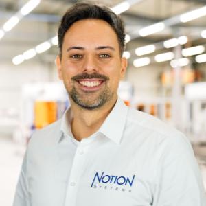
Simon Rihm
Senior Process Development Engineer
Electrohydrodynamic (EHD) printing is rapidly emerging as a transformative technology in the field of advanced electronics, offering unprecedented resolution, material versatility, and scalability. This talk explores how EHD printing leverages electric fields to precisely deposit functional inks at the microscale, enabling the fabrication of high-performance electronic components on flexible, stretchable, and unconventional substrates.
We will delve into the core principles of EHD printing, highlight recent breakthroughs in multi-nozzle printhead design, and showcase real-world applications. Attendees will gain insights into how EHD printing is overcoming limitations of traditional lithography and inkjet methods, paving the way for next-generation electronics with enhanced functionality and reduced environmental impact
High-Resolution, High-Impact: EHD Printing for Advanced Electronics
3:00 pm
Electrohydrodynamic (EHD) printing is rapidly emerging as a transformative technology in the field of advanced electronics, offering unprecedented resolution, material versatility, and scalability. This talk explores how EHD printing leverages electric fields to precisely deposit functional inks at the microscale, enabling the fabrication of high-performance electronic components on flexible, stretchable, and unconventional substrates.
We will delve into the core principles of EHD printing, highlight recent breakthroughs in multi-nozzle printhead design, and showcase real-world applications. Attendees will gain insights into how EHD printing is overcoming limitations of traditional lithography and inkjet methods, paving the way for next-generation electronics with enhanced functionality and reduced environmental impact
HighLine Technology Gmbh


Maximilian Pospischil
Managing Director
Since 2019, HighLine has been redefining PV metallization with ultra-precise fine lines up to <20 μm at dispensing speeds beyond 500 mm/s. Today, our portfolio extends from scalable dispensing to intermittent coating solutions, supported by customized nozzle kits and versatile MONO & MULTI print head systems.
With intelligent automation – from integrated cuckoo units to AI-driven recipe optimization – HighLine empowers next-level production across industries.
Next-Gen Dispensing – From Ultra-Fine Metallization to Smart Coating
3:15 pm
Since 2019, HighLine has been redefining PV metallization with ultra-precise fine lines up to <20 μm at dispensing speeds beyond 500 mm/s. Today, our portfolio extends from scalable dispensing to intermittent coating solutions, supported by customized nozzle kits and versatile MONO & MULTI print head systems.
With intelligent automation – from integrated cuckoo units to AI-driven recipe optimization – HighLine empowers next-level production across industries.
SUSS MicroTec Solutions


Dennis Kuppens
Product Manager
This presentation introduces a novel high-precision inkjet printer designed for advanced printed electronics applications. The system features a flexible printhead configuration, next to the dozen existing printhead types the machine already supports, now integrating a printhead for ultra-fine resolution (3.5 picoliter droplets) and an printhead that accommodates up to eight different inks, including water-based formulations crucial for pharmaceutical applications. This unique setup enables both highly detailed micro-printing and versatile multi-material deposition, significantly enhancing research capabilities in printed electronics and opening new avenues for scientific exploration
Inkjet Printing for Semiconductor Manufacturing: A Scalable and Material Saving Solution
3:30 pm
This presentation introduces a novel high-precision inkjet printer designed for advanced printed electronics applications. The system features a flexible printhead configuration, next to the dozen existing printhead types the machine already supports, now integrating a printhead for ultra-fine resolution (3.5 picoliter droplets) and an printhead that accommodates up to eight different inks, including water-based formulations crucial for pharmaceutical applications. This unique setup enables both highly detailed micro-printing and versatile multi-material deposition, significantly enhancing research capabilities in printed electronics and opening new avenues for scientific exploration
ImageXpert


Jochen Christiaens
Inkjet printhead selection is a critical step in the development of high-performance printed electronics systems. The printhead directly impacts print resolution, material compatibility and selection, production throughput, and overall process reliability. This presentation will explore a structured approach to printhead selection tailored for advanced printed electronics applications, where functional inks must be jetted with high precision and consistency. We will examine the key parameters influencing printhead choice, including drop volume, nozzle density, waveform customization, material compatibility, and more all within the context of application-specific requirements.
We’ll compare the latest advancements from leading piezoelectric printhead technologies and highlight performance trade-offs and integration considerations for both development and production environments. Real-world case studies will be used to illustrate how different printhead architectures perform with challenging ink formulations and substrates. Attendees will leave with a clear methodology for evaluating and selecting printheads that align with their performance goals, manufacturing constraints, and future scalability.
Selecting the Right Inkjet Printhead for Advanced Electronics Applications
3:45 pm
Inkjet printhead selection is a critical step in the development of high-performance printed electronics systems. The printhead directly impacts print resolution, material compatibility and selection, production throughput, and overall process reliability. This presentation will explore a structured approach to printhead selection tailored for advanced printed electronics applications, where functional inks must be jetted with high precision and consistency. We will examine the key parameters influencing printhead choice, including drop volume, nozzle density, waveform customization, material compatibility, and more all within the context of application-specific requirements.
We’ll compare the latest advancements from leading piezoelectric printhead technologies and highlight performance trade-offs and integration considerations for both development and production environments. Real-world case studies will be used to illustrate how different printhead architectures perform with challenging ink formulations and substrates. Attendees will leave with a clear methodology for evaluating and selecting printheads that align with their performance goals, manufacturing constraints, and future scalability.
droptical GmbH


Daniel Föste
Inkjet printing nowadays has a lot of different tools for inspection of the print process. However dropwatching, which provides the most information, is mainly used for waveform optimization in the laboratory setup so far and, less commonly, as a separate checking station in a plant. This talk will sketch the current development of droptical systems to provide an inline camera inspection solution covering all nozzles of a printhead simultaneously. This ensures consistent print quality and offers a significant advantage when changing to new batches of ink. Especially in modern applications that use higher viscosity inkjet printing, this can provide huge benefits regarding process stability and early scrap detection. In addition, an inline camera offers the possibility of closed loop control.
Inline, full-printhead camera inspection for inkjet
4:00 pm
Inkjet printing nowadays has a lot of different tools for inspection of the print process. However dropwatching, which provides the most information, is mainly used for waveform optimization in the laboratory setup so far and, less commonly, as a separate checking station in a plant. This talk will sketch the current development of droptical systems to provide an inline camera inspection solution covering all nozzles of a printhead simultaneously. This ensures consistent print quality and offers a significant advantage when changing to new batches of ink. Especially in modern applications that use higher viscosity inkjet printing, this can provide huge benefits regarding process stability and early scrap detection. In addition, an inline camera offers the possibility of closed loop control.
Exhibition & Refreshment Break
joint
Exhibition & Refreshment Break
4:15 pm
Exhibition & Refreshment Break
Abstract
Exhibition & Refreshment Break
4:15 pm
VTT Technical Research Centre of Finland

Antti Kemppainen
Visible
Printed and hybrid electronics has been introduced in various application during last years on flexible and even elastic substrates - even in roll processes. One obstacle in development has been significant costs and time needed in concept and prototyping phase. In this presentation advances in assembly, converting and characterization for faster prototyping is discussed.
Printed hybrid electronics accelerated concepting and verification
4:45 pm
Printed and hybrid electronics has been introduced in various application during last years on flexible and even elastic substrates - even in roll processes. One obstacle in development has been significant costs and time needed in concept and prototyping phase. In this presentation advances in assembly, converting and characterization for faster prototyping is discussed.
Fraunhofer IFAM


Jonas Deitschun
Printed multilayer PCBs can have significant environmental advantages over traditional FR4 circuit boards. Nevertheless, there are considerable challenges in achieving a similar level of complexity and reliability.
Hybrid electronics compared to conventional PCBs: their advantages and challenges
5:00 pm
Printed multilayer PCBs can have significant environmental advantages over traditional FR4 circuit boards. Nevertheless, there are considerable challenges in achieving a similar level of complexity and reliability.
RISE Research Institutes of Sweden AB


Duncan Platt
Group Manager
Printed electronics is an emerging field that promises to revolutionize various industries with its potential for creating flexible, lightweight, and cost-effective electronic devices. However, despite its significant advantages, many researchers and developers encounter substantial hurdles when trying to get started in this domain. These challenges include limited access to specialized materials and equipment, a steep learning curve associated with understanding the intricate fabrication processes, and the need for interdisciplinary knowledge spanning electronics, materials science, and engineering. To address these barriers, it is vital to develop deep knowledge, foster collaborative initiatives, and streamline access to essential tools and materials.
Hybrid printed electronics, which combine traditional silicon-based components with printed electronic elements, present a compelling pathway to enhance device functionality, form factor and performance. By daring to explore hybrid approaches, developers can leverage the strengths of both conventional and printed electronics to create innovative solutions.
We will discuss how to reduce the hurdles and get started with printed electronics and hybrid electronics. By encouraging experiments with hybrid designs and collaborative networks that bridge gaps between different areas of expertise, as well as with improved access to materials and equipment, we can together create new innovations.
How to get started with hybrid printed electronics
5:15 pm
Printed electronics is an emerging field that promises to revolutionize various industries with its potential for creating flexible, lightweight, and cost-effective electronic devices. However, despite its significant advantages, many researchers and developers encounter substantial hurdles when trying to get started in this domain. These challenges include limited access to specialized materials and equipment, a steep learning curve associated with understanding the intricate fabrication processes, and the need for interdisciplinary knowledge spanning electronics, materials science, and engineering. To address these barriers, it is vital to develop deep knowledge, foster collaborative initiatives, and streamline access to essential tools and materials.
Hybrid printed electronics, which combine traditional silicon-based components with printed electronic elements, present a compelling pathway to enhance device functionality, form factor and performance. By daring to explore hybrid approaches, developers can leverage the strengths of both conventional and printed electronics to create innovative solutions.
We will discuss how to reduce the hurdles and get started with printed electronics and hybrid electronics. By encouraging experiments with hybrid designs and collaborative networks that bridge gaps between different areas of expertise, as well as with improved access to materials and equipment, we can together create new innovations.
END
joint
END
5:30 pm
END
Abstract
END
5:30 pm
Track 3
Title of Talk

joint
SCIL Nanoimprint B.V.
1:30 pm
Compact AR Smart Glasses with Direct Nanoimprinted Optical Elements for MicroLED Display Integration
Abstract

Marc Verschuuren
CTO
As augmented reality (AR) smart glasses advance toward smaller, lighter, and more ergonomic designs, the integration of microLED displays introduces challenges in optical system design. Achieving a compact form factor while maintaining high image quality requires precise control over how light is extracted, coupled, and guided from microLED sources through the optical path to the visual user experience.
SCIL Nanoimprint Solutions has developed a high-precision nanoimprinting technology that enables the direct patterning of structures directly into inorganic high refractive index materials—critical for coupling light efficiently from microLED arrays into waveguides or combiners. This technique supports high-volume manufacturing of complex optical elements for both the microLED source (such as photonic crystals, plasmonics) and the waveguide combiner (slanted gratings with continuously varying depth and duty cycle), which are essential for optimizing light extraction and uniformity. The process offers great design flexibility and allows for multi-orientation patterning in a single imprint step, enabling compact, high-efficiency sources and optics that meet the challenging requirements of microLED-based optical systems. Combining advanced nanoimprint lithography with microLED display integration paves the way for scalable, high-throughput manufacturing of next-generation AR optics.
Compact AR Smart Glasses with Direct Nanoimprinted Optical Elements for MicroLED Display Integration
1:30 pm
As augmented reality (AR) smart glasses advance toward smaller, lighter, and more ergonomic designs, the integration of microLED displays introduces challenges in optical system design. Achieving a compact form factor while maintaining high image quality requires precise control over how light is extracted, coupled, and guided from microLED sources through the optical path to the visual user experience.
SCIL Nanoimprint Solutions has developed a high-precision nanoimprinting technology that enables the direct patterning of structures directly into inorganic high refractive index materials—critical for coupling light efficiently from microLED arrays into waveguides or combiners. This technique supports high-volume manufacturing of complex optical elements for both the microLED source (such as photonic crystals, plasmonics) and the waveguide combiner (slanted gratings with continuously varying depth and duty cycle), which are essential for optimizing light extraction and uniformity. The process offers great design flexibility and allows for multi-orientation patterning in a single imprint step, enabling compact, high-efficiency sources and optics that meet the challenging requirements of microLED-based optical systems. Combining advanced nanoimprint lithography with microLED display integration paves the way for scalable, high-throughput manufacturing of next-generation AR optics.
Title of Talk

joint
DR Laser Singapore Pte Ltd
1:45 pm
Laser Technologies Powering MicroLED Manufacturing
Abstract

Edmond Soh
MicroLED is heralded as the future of display technology, promising to disrupt the market currently dominated by LCD and OLED technologies. The recent first-ever commercialisation of MicroLED smartwatch highlights how this technology is moving from the lab to the consumer market. Yet, to truly unlock the full potential of MicroLED, the industry must overcome key challenges in finding a ‘killer application’ while taking into accounts of the manufacturing costs.
In this presentation, we share ideas about how MicroLED technology can be indispensable in creating potential bestseller products, and how advanced laser technologies are driving the next wave of MicroLED manufacturing. Using lasers for mass transfer and bonding, manufacturers can achieve faster production, higher yields, and greater design flexibility — bringing MicroLED closer to mainstream adoption.
Laser Technologies Powering MicroLED Manufacturing
1:45 pm
MicroLED is heralded as the future of display technology, promising to disrupt the market currently dominated by LCD and OLED technologies. The recent first-ever commercialisation of MicroLED smartwatch highlights how this technology is moving from the lab to the consumer market. Yet, to truly unlock the full potential of MicroLED, the industry must overcome key challenges in finding a ‘killer application’ while taking into accounts of the manufacturing costs.
In this presentation, we share ideas about how MicroLED technology can be indispensable in creating potential bestseller products, and how advanced laser technologies are driving the next wave of MicroLED manufacturing. Using lasers for mass transfer and bonding, manufacturers can achieve faster production, higher yields, and greater design flexibility — bringing MicroLED closer to mainstream adoption.
Title of Talk


Kahraman Keskinbora
Senior Application Engineer
High-resolution, high-throughput laser lithography is emerging as a critical technology for bridging the gap between research and industrial adoption in advanced device manufacturing. Leveraging maskless, direct-write flexibility, modern systems integrate multi-beam parallelization, high-NA optics, and precision stage control to deliver deep-sub-micron resolution while maintaining large-area scalability.
These advancements open new opportunities in semiconductor and photonics markets where both speed and fidelity are essential. In microLEDs, laser lithography enables rapid prototyping and high-volume master fabrication for mass transfer processes. In advanced packaging, it supports redistribution layers and through-package vias with fine-pitch accuracy. For photonic components, grayscale lithography extends the platform to 3D topographies such as waveguides and microlens arrays, critical for AR/VR and optical communication systems. Here in this talk, we will go into the details how the parallel maskless laser lithography engines can provide real-time grayscale exposure while providing a deep sub-micron resolution and excellent overlay capabilities for applications in micro-optics, mask making and advanced packaging.
By combining throughput, resolution, and process versatility, next-generation laser lithography provides a cost-effective alternative to mask-based approaches, accelerating innovation from concept to pilot-line production.
High Resolution and High Throughput Laser Lithography
2:00 pm
High-resolution, high-throughput laser lithography is emerging as a critical technology for bridging the gap between research and industrial adoption in advanced device manufacturing. Leveraging maskless, direct-write flexibility, modern systems integrate multi-beam parallelization, high-NA optics, and precision stage control to deliver deep-sub-micron resolution while maintaining large-area scalability.
These advancements open new opportunities in semiconductor and photonics markets where both speed and fidelity are essential. In microLEDs, laser lithography enables rapid prototyping and high-volume master fabrication for mass transfer processes. In advanced packaging, it supports redistribution layers and through-package vias with fine-pitch accuracy. For photonic components, grayscale lithography extends the platform to 3D topographies such as waveguides and microlens arrays, critical for AR/VR and optical communication systems. Here in this talk, we will go into the details how the parallel maskless laser lithography engines can provide real-time grayscale exposure while providing a deep sub-micron resolution and excellent overlay capabilities for applications in micro-optics, mask making and advanced packaging.
By combining throughput, resolution, and process versatility, next-generation laser lithography provides a cost-effective alternative to mask-based approaches, accelerating innovation from concept to pilot-line production.
Title of Talk


Lucas Klamer
Co-Founder
The promise of Augmented Reality is vast, but a critical challenge remains: billions of potential users wear prescription glasses. Existing AR solutions often fall short, forcing uncomfortable workarounds or excluding those with vision correction altogether. This limits adoption and hinders the true potential of AR.
Direct Finished Lens Casting Technology creates thin and lightweight prescription lenses with integrated waveguide displays.
The Direct Finished Lens Casting Technology allows for the combination of prescription corrected lenses and integrated mechanical features while minimizing weight and volume.
Furthermore, it eliminates the need for edging and polishing, which in turn allows for complex freeform surfaces. Finally, the process is set-up to embed electronic components into the lens. Together this results in the most advanced prescription lenses for AR glasses.
Creating the world's most advanced prescription lens technology for Augmented Reality glasses
2:15 pm
The promise of Augmented Reality is vast, but a critical challenge remains: billions of potential users wear prescription glasses. Existing AR solutions often fall short, forcing uncomfortable workarounds or excluding those with vision correction altogether. This limits adoption and hinders the true potential of AR.
Direct Finished Lens Casting Technology creates thin and lightweight prescription lenses with integrated waveguide displays.
The Direct Finished Lens Casting Technology allows for the combination of prescription corrected lenses and integrated mechanical features while minimizing weight and volume.
Furthermore, it eliminates the need for edging and polishing, which in turn allows for complex freeform surfaces. Finally, the process is set-up to embed electronic components into the lens. Together this results in the most advanced prescription lenses for AR glasses.
Title of Talk
joint
Exhibition & Refreshment Break
2:30 PM
Exhibition & Refreshment Break
Abstract
Exhibition & Refreshment Break
2:30 PM
Title of Talk


Ivan-Christophe Robin
Head of Innovation
A new kind of microLEDs’ array technology that aims to answer ultrahigh brightness, narrow optical aperture, low power consumption and small footprint requirements for Augmented Reality glasses applications will be discussed.
GaN sub-micrometer (“nano”) rods are grown directly on large size microelectronic silicon wafers with further LED structure resulting in self-standing “nanoLEDs”. NanoLEDs size allows to array them in such a way it builds a photonic crystal tuned to the desired emission wavelength and designed so that propagative modes are only allowed into a narrow cone normal to the array plane. It results in intrinsic directivity of light emission without a need for additional microlenses, meaning that instead of losing 90% of the light not entering the AR glasses optics (waveguides, for instance) most of it becomes useful raising significantly the overall system power efficiency. The number of nanoLEDs to maintain efficient photonic effect is discussed and leads to µm range subpixel capability, other advantageous consequences of such a resonant coupling are discussed, while single color arrays results are presented.
Furthermore, quantum well Indium composition can be modulated by playing on local fill-factor, basically size and pitch of the nanorods, thus changing the quantum well emission wavelength. By adding fill-factor constrain to photonic crystal design for directivity it is possible to grow in a single run three colors (R,G,B) patterns with most of above advantages, including directivity of light emission. Design trade-off and perspectives are discussed and results on actual microLEDs presented. This technology opens path to single chip >6000ppi RGB ultra-compact and highly efficient micro display designs.
MicroLEDs with built-in directive emission and RGB capability for power efficient AR microdisplays
3:00 pm
A new kind of microLEDs’ array technology that aims to answer ultrahigh brightness, narrow optical aperture, low power consumption and small footprint requirements for Augmented Reality glasses applications will be discussed.
GaN sub-micrometer (“nano”) rods are grown directly on large size microelectronic silicon wafers with further LED structure resulting in self-standing “nanoLEDs”. NanoLEDs size allows to array them in such a way it builds a photonic crystal tuned to the desired emission wavelength and designed so that propagative modes are only allowed into a narrow cone normal to the array plane. It results in intrinsic directivity of light emission without a need for additional microlenses, meaning that instead of losing 90% of the light not entering the AR glasses optics (waveguides, for instance) most of it becomes useful raising significantly the overall system power efficiency. The number of nanoLEDs to maintain efficient photonic effect is discussed and leads to µm range subpixel capability, other advantageous consequences of such a resonant coupling are discussed, while single color arrays results are presented.
Furthermore, quantum well Indium composition can be modulated by playing on local fill-factor, basically size and pitch of the nanorods, thus changing the quantum well emission wavelength. By adding fill-factor constrain to photonic crystal design for directivity it is possible to grow in a single run three colors (R,G,B) patterns with most of above advantages, including directivity of light emission. Design trade-off and perspectives are discussed and results on actual microLEDs presented. This technology opens path to single chip >6000ppi RGB ultra-compact and highly efficient micro display designs.
Title of Talk

Jasper Wesselingh
Senior Principal Mechatronics Architect
High-yield and cost-effective microLED assembly processes still face major challenges to solve for successful market adoption by the display and lighting markets. We believe that achieving five-nine (or even six-nine) yield is within reach—enabled by 100% in-line quality control and in-cycle process selectivity for both placement and binning. ITEC has been working together with TNO-Holst to bring two key processes to market: LIFT2.0 for dispensing of interconnect materials and FAST-CT for laser component transfer.We developed the XG-Alpha, a lab tool that enables fast turn-around in sample making for MicroLED applications. It is a flexible platform combining laser-based micro-droplet dispensing and laser-based die transfer. The tool offers a flexibility in input materials, inline metrology for placement position-alignment, dynamic transfer gap control, and automatic setting of the laser spot dimensions. For quality inspection and process windowing, it is equipped with 100% automatic optical inspection of donor and receiver substrates, and single shot repair functionality.
This presentation discusses the features of this tool, how it aligns to the process development roadmap of TNO. Furthermore it is the beginning of ITEC’s journey toward building the XG-platform as an industrial enabler for next-generation MicroLED manufacturing. We invite industry partners to explore the XG-alpha tool for their specific applications and join us in shaping the future of MicroLED production.
XG-Alpha: Exploring Cost-Effective, High-Quality Laser Assembly of MicroLEDs
3:15pm
High-yield and cost-effective microLED assembly processes still face major challenges to solve for successful market adoption by the display and lighting markets. We believe that achieving five-nine (or even six-nine) yield is within reach—enabled by 100% in-line quality control and in-cycle process selectivity for both placement and binning. ITEC has been working together with TNO-Holst to bring two key processes to market: LIFT2.0 for dispensing of interconnect materials and FAST-CT for laser component transfer.We developed the XG-Alpha, a lab tool that enables fast turn-around in sample making for MicroLED applications. It is a flexible platform combining laser-based micro-droplet dispensing and laser-based die transfer. The tool offers a flexibility in input materials, inline metrology for placement position-alignment, dynamic transfer gap control, and automatic setting of the laser spot dimensions. For quality inspection and process windowing, it is equipped with 100% automatic optical inspection of donor and receiver substrates, and single shot repair functionality.
This presentation discusses the features of this tool, how it aligns to the process development roadmap of TNO. Furthermore it is the beginning of ITEC’s journey toward building the XG-platform as an industrial enabler for next-generation MicroLED manufacturing. We invite industry partners to explore the XG-alpha tool for their specific applications and join us in shaping the future of MicroLED production.
Title of Talk


Susan
Commercially available visible wavelength LEDs originated in the 1960s and yet sixty years later, there is still a huge amount of research and investment in this sector. Technological and environmental advances necessitate device miniaturisation, higher light output, reduced power consumption, faster switching and improved colour gamut. While advanced fabrication and processing techniques meet some of these new challenges, the complexity and associated costs of manufacturing microLEDs with such requirements have stalled the widespread adoption of microLEDs across various market sectors.
At Kubos Semiconductors we are focused on a material-level solution, using cubic-GaN, to overcome the fundamental technological limitations that have hindered market adoption. This presentation will explain the unique properties of cubic-GaN that make it a material of choice for future visible wavelength LEDs and microLEDs. Furthermore, we will explain how Kubos’ technology can enhance existing device performance and enable RGB wavelength from a common material platform with minimal capital investment and process adjustment, using existing semi-standard silicon toolsets at 200mm and above.
Next generation material for microLEDs; the relevance of cubic-GaN
3:30pm
Commercially available visible wavelength LEDs originated in the 1960s and yet sixty years later, there is still a huge amount of research and investment in this sector. Technological and environmental advances necessitate device miniaturisation, higher light output, reduced power consumption, faster switching and improved colour gamut. While advanced fabrication and processing techniques meet some of these new challenges, the complexity and associated costs of manufacturing microLEDs with such requirements have stalled the widespread adoption of microLEDs across various market sectors.
At Kubos Semiconductors we are focused on a material-level solution, using cubic-GaN, to overcome the fundamental technological limitations that have hindered market adoption. This presentation will explain the unique properties of cubic-GaN that make it a material of choice for future visible wavelength LEDs and microLEDs. Furthermore, we will explain how Kubos’ technology can enhance existing device performance and enable RGB wavelength from a common material platform with minimal capital investment and process adjustment, using existing semi-standard silicon toolsets at 200mm and above.
Title of Talk

joint
VueReal
3:45 pm
Human–Machine Interface (HMI) needs in the age of AI and immersive applications
Abstract

Reza Chaji
CEO
The rapid convergence of artificial intelligence and immersive technologies is reshaping how humans interact with machines. In this talk, I will explore the evolving requirements of Human–Machine Interfaces (HMI) to enable intuitive, seamless, and context-aware experiences across automotive, wearable, and consumer applications. I will discuss how AI-driven personalization, multimodal sensing, and real-time adaptive feedback are redefining user expectations, and why display and interaction technologies must evolve to meet the demands of extended reality (XR), connected mobility, and smart environments. By highlighting both the challenges—such as transparency, power efficiency, and safety—and the opportunities—such as microdisplay integration, natural interaction, and scalable architectures—this session will outline a roadmap for next-generation HMIs that bridge digital intelligence with human experience.
Human–Machine Interface (HMI) needs in the age of AI and immersive applications
3:45 pm
The rapid convergence of artificial intelligence and immersive technologies is reshaping how humans interact with machines. In this talk, I will explore the evolving requirements of Human–Machine Interfaces (HMI) to enable intuitive, seamless, and context-aware experiences across automotive, wearable, and consumer applications. I will discuss how AI-driven personalization, multimodal sensing, and real-time adaptive feedback are redefining user expectations, and why display and interaction technologies must evolve to meet the demands of extended reality (XR), connected mobility, and smart environments. By highlighting both the challenges—such as transparency, power efficiency, and safety—and the opportunities—such as microdisplay integration, natural interaction, and scalable architectures—this session will outline a roadmap for next-generation HMIs that bridge digital intelligence with human experience.
Title of Talk

Andrew Munro
MicroLED displays are poised to revolutionize the automotive industry, delivering improved performance. As production techniques improve and costs decrease, microLED technology will become more pervasive in Head-Up Displays (HUDs), intelligent adaptive headlights, customizable exterior lighting, and cockpit displays.
Metrology of microLED next-generation automotive interfaces is of utmost importance to ensure their successful implementation. Performance metrics include emitter defects, luminance and color non-uniformity, and much more. Solutions for the calibration and testing of microLED products that streamline the quality control process must adequately meet the inspection challenges. These can include a non-uniformity correction process (demura) to actively balance the display to a target uniformity, while also testing for performance metrics to pass/fail the display, and hitting cycle time.
The automotive industry poses an interesting opportunity for microLED developers who can provide a compelling solution for next-generation automotive displays and lighting. Proper implementation of metrology will help microLED developers to deliver the quality of product needed for succeed in this market.
Addressing the Visual Inspection Challenges of microLED Displays & Lighting in Vehicles
4:00 PM
MicroLED displays are poised to revolutionize the automotive industry, delivering improved performance. As production techniques improve and costs decrease, microLED technology will become more pervasive in Head-Up Displays (HUDs), intelligent adaptive headlights, customizable exterior lighting, and cockpit displays.
Metrology of microLED next-generation automotive interfaces is of utmost importance to ensure their successful implementation. Performance metrics include emitter defects, luminance and color non-uniformity, and much more. Solutions for the calibration and testing of microLED products that streamline the quality control process must adequately meet the inspection challenges. These can include a non-uniformity correction process (demura) to actively balance the display to a target uniformity, while also testing for performance metrics to pass/fail the display, and hitting cycle time.
The automotive industry poses an interesting opportunity for microLED developers who can provide a compelling solution for next-generation automotive displays and lighting. Proper implementation of metrology will help microLED developers to deliver the quality of product needed for succeed in this market.
Title of Talk
joint
Exhibition & Refreshment Break
4:15 pm
Exhibition & Refreshment Break
Abstract
Exhibition & Refreshment Break
4:15 pm
Title of Talk


Dr Jon Carle
Perovskite solar cells are promising candidates for next-generation solar technology, but their transition from laboratory research to large-scale commercial production presents significant challenges. Scaling these technologies requires addressing issues related to efficiency, material costs, resource consumption, and long-term sustainability—all of which affect the overall cost-effectiveness and viability of manufacturing processes. While early research focuses on innovation and technological development, achieving commercialization demands solutions that ensure both scalability and processing flexibility. By employing advanced techniques and equipment—such as laboratory-scale sheet coaters and roll-to-roll coaters—researchers and manufacturers can better address these challenges and facilitate the successful commercialization of perovskite solar technologies.
Innovations in Processing Techniques for Perovskite Solar Cells
4:45 pm
Perovskite solar cells are promising candidates for next-generation solar technology, but their transition from laboratory research to large-scale commercial production presents significant challenges. Scaling these technologies requires addressing issues related to efficiency, material costs, resource consumption, and long-term sustainability—all of which affect the overall cost-effectiveness and viability of manufacturing processes. While early research focuses on innovation and technological development, achieving commercialization demands solutions that ensure both scalability and processing flexibility. By employing advanced techniques and equipment—such as laboratory-scale sheet coaters and roll-to-roll coaters—researchers and manufacturers can better address these challenges and facilitate the successful commercialization of perovskite solar technologies.
Title of Talk

Alexander Bouman
A key challenge in scaling perovskite solar cells (PSCs) lies in the high-throughput and uniform deposition of thin films such as SnO₂ electron transport layers on flexible substrates. Conventional ALD provides excellent film quality but suffers from low throughput due to slow pump–purge cycles and limited area. Spatial ALD overcomes this by separating precursor exposures, enabling deposition rates over two orders of magnitude faster in combination with a roll-to-roll format. With web speeds support up to 80 m·min⁻¹, substrate widths up to 1.5 m, and deposition temperatures between 50–150 °C for flexible polymer and metal foils, the key challenge can be resolved. This presentation will introduce the fundamentals of spatial ALD and illustrate how the roll-to-roll implementation enables translation from laboratory-scale film optimization to gigawatt-scale PSC manufacturing, with emphasis on scalable SnO₂ deposition and how the SparkNano Omega system addresses the throughput, uniformity, and substrate compatibility requirements critical for industrialization.
Roll-to-Roll spatial ALD advances scalable perovskite solar cell manufacturing
5:00 PM
A key challenge in scaling perovskite solar cells (PSCs) lies in the high-throughput and uniform deposition of thin films such as SnO₂ electron transport layers on flexible substrates. Conventional ALD provides excellent film quality but suffers from low throughput due to slow pump–purge cycles and limited area. Spatial ALD overcomes this by separating precursor exposures, enabling deposition rates over two orders of magnitude faster in combination with a roll-to-roll format. With web speeds support up to 80 m·min⁻¹, substrate widths up to 1.5 m, and deposition temperatures between 50–150 °C for flexible polymer and metal foils, the key challenge can be resolved. This presentation will introduce the fundamentals of spatial ALD and illustrate how the roll-to-roll implementation enables translation from laboratory-scale film optimization to gigawatt-scale PSC manufacturing, with emphasis on scalable SnO₂ deposition and how the SparkNano Omega system addresses the throughput, uniformity, and substrate compatibility requirements critical for industrialization.
Title of Talk


Nicolas Vandamme
Integration, Prototyping Platform Manager
IPVF is developing perovskite technologies in the Paris-Saclay area (France) as part of its comprehensive R&D program on photovoltaics, semiconductors and photonics. In 2025, IPVF is building a new lab2fab technological platform to produce 30x60 cm² perovskite modules. 500 m² of cleanrooms are dedicated to the pursuit of best efficiencies, with the possibility to test new materials and new processes at each stage of the fabrication. We will present the line as well as upcoming and expected outcomes, as the platform may also be used by our partners.
STAFF: the new lab2fab platform for pervokiste development in Europe
5:15 pm
IPVF is developing perovskite technologies in the Paris-Saclay area (France) as part of its comprehensive R&D program on photovoltaics, semiconductors and photonics. In 2025, IPVF is building a new lab2fab technological platform to produce 30x60 cm² perovskite modules. 500 m² of cleanrooms are dedicated to the pursuit of best efficiencies, with the possibility to test new materials and new processes at each stage of the fabrication. We will present the line as well as upcoming and expected outcomes, as the platform may also be used by our partners.
Title of Talk
joint
Exhibition & Refreshment Break
5:30 pm
Exhibition & Refreshment Break
Abstract
Exhibition & Refreshment Break
5:30 pm
Title of Talk


Varun Vohra
R&D Director
As energy demands rise, organic photovoltaics (OPVs) offer a versatile, rapidly manufactured solution with a low energy payback time and low carbon footprint. Lightweight, flexible, and semi-transparent, OPVs are applicable in agrivoltaics, building integration technologies, and for low intensity light harvesting for IoT devices.
This talk will highlight our work in developing scalable active-layer materials for industrially produced OPV panels. Here, we will present our newest active layer blend, which has been designed to deliver over 10% power conversion efficiency at the module level. The novel active layer exhibits exceptional stability under continuous light-soaking tests and has a scalable and reproducible synthesis allowing for production at the high volumes which are critical for mass production of OPV. Initial results, including batch to batch reproducibility, device performance and stability testing will be discussed alongside the targeted applications for this unique technology.
A Scalable Active Layer System Delivering a Stabilized 10% Power Conversion Efficiency for Commercial Organic Photovoltaics
6:00PM
As energy demands rise, organic photovoltaics (OPVs) offer a versatile, rapidly manufactured solution with a low energy payback time and low carbon footprint. Lightweight, flexible, and semi-transparent, OPVs are applicable in agrivoltaics, building integration technologies, and for low intensity light harvesting for IoT devices.
This talk will highlight our work in developing scalable active-layer materials for industrially produced OPV panels. Here, we will present our newest active layer blend, which has been designed to deliver over 10% power conversion efficiency at the module level. The novel active layer exhibits exceptional stability under continuous light-soaking tests and has a scalable and reproducible synthesis allowing for production at the high volumes which are critical for mass production of OPV. Initial results, including batch to batch reproducibility, device performance and stability testing will be discussed alongside the targeted applications for this unique technology.
Title of Talk


Maryam Bari
CEO
PINA’s printable ZnO and SnO₂ nano inks maximize perovskite solar cell efficiency by 20%, boost durability by 50%, and enable cost-effective, scalable production on glass and flexible substrates.
A key barrier to the commercialization of perovskite solar cells (PSCs) lies in translating high laboratory efficiencies into stable, large-area devices manufactured at scale. The performance and lifetime of PSCs critically depend on the electron transport layer (ETL) and hole transport layer (HTL), which must combine high optoelectronic quality with compatibility for industrial coating methods. PINA Creation addresses this challenge with advanced ZnO and SnO₂ nano inks—water-based and alcohol-based formulations engineered for slot-die, roll-to-roll, inkjet, blade, and spin coating on both glass and flexible substrates. Our low-temperature (<150 °C), high-transparency (>85%), cost-effective ETLs have been shown to improve solar cell efficiency by up to 20% and increase durability by 50% compared to traditional materials. By enabling scalable, high-performance, and eco-friendly ETL solutions, PINA bridges the gap between lab-scale prototypes and commercial perovskite module production.
Bridging the Lab-to-Fab Gap: HowTin Oxide Nano Inks Drive Perovskite Commercialization?
6:15 pm
PINA’s printable ZnO and SnO₂ nano inks maximize perovskite solar cell efficiency by 20%, boost durability by 50%, and enable cost-effective, scalable production on glass and flexible substrates.
A key barrier to the commercialization of perovskite solar cells (PSCs) lies in translating high laboratory efficiencies into stable, large-area devices manufactured at scale. The performance and lifetime of PSCs critically depend on the electron transport layer (ETL) and hole transport layer (HTL), which must combine high optoelectronic quality with compatibility for industrial coating methods. PINA Creation addresses this challenge with advanced ZnO and SnO₂ nano inks—water-based and alcohol-based formulations engineered for slot-die, roll-to-roll, inkjet, blade, and spin coating on both glass and flexible substrates. Our low-temperature (<150 °C), high-transparency (>85%), cost-effective ETLs have been shown to improve solar cell efficiency by up to 20% and increase durability by 50% compared to traditional materials. By enabling scalable, high-performance, and eco-friendly ETL solutions, PINA bridges the gap between lab-scale prototypes and commercial perovskite module production.
Title of Talk


Miguel Friedrich
Chief Business Development Officer
Perovskite solar cells (PSC) have demonstrated remarkable efficiency gains in a relatively short timeframe, setting the stage for their potential in large-scale production. However, as companies strive to scale PSC to large area processing (1x2 meters panels or larger) for mass production (single junction and 4-terminal), several challenges emerge.
Challenges in scaling Perovskite to Mass Production
6:30 pm
Perovskite solar cells (PSC) have demonstrated remarkable efficiency gains in a relatively short timeframe, setting the stage for their potential in large-scale production. However, as companies strive to scale PSC to large area processing (1x2 meters panels or larger) for mass production (single junction and 4-terminal), several challenges emerge.
Title of Talk
joint
END
6:45 pm
END
Abstract
END
6:45 pm