
top of page


1/4


24 July 2026
Introducing the Program – Rethinking the PCB: Wearables That Work: Health, Safety & Performance
Why Should You Join TechBlick's The Future of Electronic Textiles RESHAPED? The Future of Electronic Textiles RESHAPED conference and exhibition (21 & 22 OCT 2026, Estrel Congress Centre, Berlin) is where technologies and applications meet, accelerating the industrialisation of smart and electronic textiles. The event is co-located with Electronics RESHAPED, Sustainable Electronics RESHAPED, and Perovskite Connect. Smart textiles prove their worth on the body — monitoring health, protecting workers, and performing in environments where conventional electronics fail. In this article, we highlight talks around the theme of wearables that work: health and physiological monitoring, and safety-critical wearables for demanding environments. In a companion article, we cover the manufacturing platforms, materials, and standards behind these products. Explore the full agenda now and register to join the event — one pass gives you access to all four co-located shows, the exhibition, and the TechBlick on-demand library. Health & Physiological Monitoring: From Lab Accuracy to Daily Wear Danish Technological Institute (Denmark) – Zachary J. Davis provides a comprehensive overview of DTI's smart wearable technologies, spanning the full value chain from e-textile manufacturing and standardized IPC test methods (wash durability, abrasion, tensile and stretch behavior, climate exposure) to functional demonstrators: a printed EMG electrode sleeve targeting musculoskeletal disorder prevention w...

22 July 2026
Introducing the Program – Rethinking the PCB: Sustainable Substrates & Greener Production
Why Should You Join TechBlick's Sustainable Electronics RESHAPED? Sustainable Electronics RESHAPED (21 & 22 OCT 2026, Estrel Congress Centre, Berlin) is where the global sustainable electronics industry takes form — reshaping the future of electronics layer by layer, through sustainable materials, efficient manufacturing, and circular designs. The event is co-located with Electronics RESHAPED, Electronic Textiles RESHAPED, and Perovskite Connect. The printed circuit board sits at the heart of electronics — and at the heart of its waste problem. In this article, we highlight talks around the theme of rethinking the PCB: bio-based substrates, additive and recyclable circuit fabrication, and greener production at industrial scale. In a companion article, we cover life cycle assessment, eco-design, and circular business models. Explore the full agenda now and register to join the event — one pass gives you access to all four co-located shows, the exhibition, and the TechBlick on-demand library. Bio-Based PCB Substrates: Wood, Cellulose, and Natural Fibres Holzforschung Austria (Austria) – Boris Forsthuber presents ecoPCBs on wood, developed within the EU-funded HyPELignum project. Conductive paths are printed onto wood substrates via inkjet or screen printing; the plywood ecoPCB concept prints circuitry into each veneer layer before gluing, connecting layers with vias to mimic a conventional multilayer PCB. Waterborne primers homogenize ink penetration on birch wood, and the scre...

30 June 2026
Agenda is live: MicroLED Connect + AR/VR Connect + Optical I/O Connect
16 & 17 September 2026 | High Tech Campus, Eindhoven, Netherlands The agenda is LIVE! It is time to explore the full agenda and book your tickets! This event will feature ✅MicroLED Connect,✅ AR/VR Connect and ✅Optical I/O Connect, uniquely bringing together the display, the semiconductor and the AI communities. The agenda is very strong, featuring the likes of Google, Microsoft, Meta, Sony, GlobalFoundries, AppliedMaterials, Samsung Display, EssilorLuxottica, Aumovio, and more. You can explore the agenda below The exhibition floor is also nearly sold out. The ground floor is in fact full and for the first time we have opened the space on the upper floor for exhibition too! 📅When: 16 & 17 Sept 2026 (Masterclasses on 15 Sept 2026) 📍Where: High Tech Campus, Eindhoven, Netherlands 📋Combined Agenda: https://www.microledconnect.com/agenda-2026 Explore LIVE Agenda Now and Book Your Tickets Day1: 16.09.2026 09:15 | Track 1 | Sony | Challenges in democratizing AR glasses 09:35 | Track 1 | Google | Purpose-Driven Pixels: Aligning Display Tech with XR Use Cases 10:10 | Track 1 | Meta | AI glasses 11:15 | Track 1 | Hongshi Intelligence | What’s Next for MicroLED Micro-Displays: Hybrid Bonding, Metasurfaces, and System-Level Iteration 11:15 | Track 2 | Lumus | Synergistic Design of Micro-LED Projectors and Waveguides 11:35 | Track 1 | Adeia | 3D System Integration for MicroLEDs: Hybrid Bonding and Co-Optimization of GaN and Silicon 11:35 | Track 2 | Optinvent | Molded Polymer Reflec...

1 June 2026
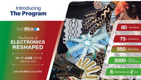
Speaker Lineup and Agenda: The Future of Electronics RESHAPED USA 2026
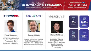
Future of Electronics RESHAPED: USA conference arrives in Mountain View, California, on 10-11 June 2026. Held at the Computer History Museum, this global gathering focuses on the commercialization and technical advancement of additive, printed, 3D, and wearable electronics. This is the most important and the largest conference and exhibition of the year dedicated to printed electronics, additive electronics, 3D electronics, wearable electronics, flexible electronics and hybrid electronics. The 2026 agenda features deep-tech presentations from industry leaders covering material innovations, scalable roll-to-roll (R2R) manufacturing, and novel hardware applications. Final early bird rates expire on 30 May. Register Now! Agenda: Link Registration: Link High-precision capillary printing, roll-to-roll VIA printing, and electrochemical additive manufacturing (ECAM) for thermal management. Sub-Micron Printing, Scalable FHE, and Next-Gen AI Cooling? Here we introduce the talks to be given in Mountain View at Day 1, Track 1, Keynote Presentations covering high-precision capillary printing, roll-to-roll VIA printing, and electrochemical additive manufacturing (ECAM) for thermal management. Hummink | Pascal Boncenne Topic: HPCaP (High Precision Capillary Printing) : A Technology for Advanced Packaging. Pascal explores the strict micron-scale limitations of traditional inkjet printing, which relies on external lasers, pressure, or UV energy and struggles with high-viscosity materials. Th...

24 July 2026
Introducing the Program – Materials and Films Innovations for Perovskite Solar
Why Should You Join TechBlick's Perovskite Connect? Perovskite Connect (21 & 22 OCT 2026, Estrel Congress Centre, Berlin) brings together the companies, institutes, and equipment makers turning perovskite photovoltaics from a laboratory success story into a manufacturable, bankable product. The event is co-located with Electronics RESHAPED, Electronic Textiles RESHAPED, and Sustainable Electronics RESHAPED. A perovskite module is a stack of thin layers, and every one of them is a materials problem: transport layers that must be depositable at scale, contacts that survive firing, encapsulants that keep moisture out for 25 years, and electrodes that don't depend on scarce indium. In this article, we highlight talks around the theme of materials innovations — charge transport and interfaces, encapsulation and end-of-life, and transparent electrodes and alternative device concepts. In companion articles, we cover tandems and commercial deployment, and manufacturing equipment and processes. Explore the full agenda and register early for the best rates — one pass gives you access to all four co-located shows, the exhibition, and the TechBlick on-demand library. Charge Transport & Interface Materials TU Dortmund (Germany) – Matthias Grotevent presents a room-temperature synthesis of crystalline tin oxide nanocrystals that is remarkably robust: particle size and crystallinity are independent of reaction time, temperature, and precursor concentration. Unlike conventional colloidal syn...

21 July 2026
Introducing the Program – Breaking Barriers in Digital Deposition & Inkjet
Why Should You Join TechBlick's The Future of Electronics RESHAPED? The Future of Electronics RESHAPED conference and exhibition (21 & 22 OCT 2026, Estrel Congress Centre, Berlin) is set to be the most important event of the year focused on additive, hybrid, 3D, sustainable, wearable, soft and textile electronics. The event is co-located with Electronic Textiles RESHAPED, Sustainable Electronics RESHAPED, and Perovskite Connect, bringing the entire ecosystem together under one roof. In this article, we highlight a series of superb talks around the theme of digital deposition and inkjet printing — from printheads that finally break the viscosity barrier, to complete digital manufacturing platforms, to technologies that push additive precision down to the sub-micron level. In future articles, we will cover further themes including material, ink and paste innovations; manufacturing and hybrid integration; and printed electronics applications. Explore the full agenda now and register to join the event — one pass gives you access to all four co-located shows, the exhibition, and the TechBlick on-demand library. Breaking the Viscosity Barrier: Next-Generation Inkjet Printheads For decades, inkjet in electronics has been confined to low-viscosity, near-Newtonian fluids, leaving most functional pastes to analogue screen printing. In Berlin, four leading printhead makers will show how this decades-old limit is finally falling. XAAR (United Kingdom) – Karl Forbes examines how recent ad...
24 June 2026
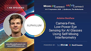
AlphaLum | What if the biggest bottleneck holding back the mass commercialization of all-day-wearable AI glasses isn't the display itself, but the way we track the use...
What if the biggest bottleneck holding back the mass commercialization of all-day-wearable AI glasses isn't the display itself, but the way we track the user's eyes? For AR OEMs, display integrators, and product strategists, the trade-off has always been brutal: resource-heavy, power-hungry camera architectures that kill battery life, or subpar, sluggish user experiences. But a massive structural paradigm shift is coming. By stripping the camera out of the equation entirely and replacing it with ultra-low-power, high-frequency temporal sensing integrated directly into the lens, a new commercial pathway is opening up. This breakthrough unlocks true "always-on" natural user interfaces at up to 1000 Hz while keeping power budgets at an absolute minimum—solving a critical hardware hurdle for consumer-grade, lightweight smart glasses and redefining the competitive roadmap for next-generation spatial computing. Join us at MicroLED Connect and AR/VR Connect at the High Tech Campus in Eindhoven (Netherlands) on 16 and 17 Sept 2026 to see how this technology is reshaping the display and AR optics landscape, and catch this presentation: * Who is presenting: Antoine Boniface; * Company: AlphaLum; * Title of the talk: Camera-Free, Low-Power Eye Sensing for AI Glasses Using Self-Mixing Interferometry; * Where they will present: High Tech Campus, Eindhoven (Netherlands); * Event & Dates: MicroLED Connect and AR/VR Connect on 16 and 17 Sept 2026; * Full Program: https://www.microledconnect....

1 June 2026
Future of Electronics RESHAPED: Smart interactive label technologies, silicone-based dry electrode biosensing, and AI-boosted neuromuscular tracking.
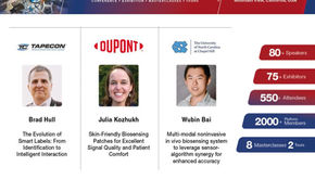
Intelligent Labels, Biosensing Patches, and Multi-Modal Tracking? Here we introduce the talks to be given in Mountain View at Day 1, Track 1, Session 1 covering smart interactive label technologies, silicone-based dry electrode biosensing, and AI-boosted neuromuscular tracking. Tapecon | Brad Hull Topic: The Evolution of Smart Labels: From Identification to Intelligent Interaction. Brad explores how standard barcoded identification no longer satisfies the data demands of modern logistics, healthcare, and retail ecosystems. The presentation outlines a versatile toolbox of emerging technologies designed to transform passive packaging into intelligent devices capable of autonomous authentication, sensing, and communication. This work provides original equipment manufacturers (OEMs) with a practical guide to speed up distributed workflows and enable real-time interactive product tracking. DuPont | Julia Kozhukh Topic: Skin-Friendly Biosensing Patches for Excellent Signal Quality and Patient Comfort. Julia explores the medical and technical challenges of remote cardiac monitoring, where standard patch materials cause skin irritation and suffer from signal degradation during extended patient wear. The talk details an innovative patch design utilizing silicone pressure-sensitive adhesives combined with specialized, silicone-based dry electrodes. This solution delivers an ultra-comfortable, skin-friendly architecture that maintains excellent signal quality to support early clinical d...
bottom of page