


ZnO Deposition with Direct Atomic Layer Processing (DALP®)
- Oct 17, 2025
- 8 min read
Authors: Laszlo Izso. Matthias Carnoy. Nandan Singh Ruhela. Benjamin Borie. Mira Baraket. Maksym Plakhotnyuk
Introduction: ZnO from an Applications point of view
Zinc oxide (ZnO) is a versatile semiconductor material that has attracted broad interest in electronics and sensing. It features a direct wide bandgap of ~3.37 eV, making it useful for UV optoelectronic devices like LEDs and photodetectors [1]. ZnO is also abundant, low-cost, and chemically stable, and it can be synthesized via relatively easy methods all contributing to its popularity in research and industry [2]. Beyond optics, ZnO can be doped to achieve high conductivity (transparent conducting films) and used in thin-film transistors (TFTs) as an n-type semiconductor channel. In microelectronics, ZnO and related oxides have been explored for transparent and flexible transistors, as well as varistors and UV sensors.
Its wurtzite crystal structure lacks inversion symmetry, giving ZnO a strong electromechanical coupling it is one of the few semiconductors that is also piezoelectric [3]. This means mechanical strain can induce an electric charge and vice versa, enabling ZnO to serve in mechanical actuators and sensors [3]. In MEMS/NEMS devices, polycrystalline ZnO thin films (often c-axis oriented) are used for piezoelectric actuators, micro-resonators, and energy harvesters. For example, ZnO thin films form the active layer in surface acoustic wave (SAW) devices and bulk acoustic resonators for filters and sensors [1].
Because of this unique mix of optical, electronic, and piezoelectric properties, ZnO attracts strong interest across multiple industries. In consumer and mobile electronics, it enables transparent and flexible displays, UV photodetectors, and low-power TFT backplanes; in automotive and industrial sensing, its piezoelectric response supports vibration, pressure, and acoustic devices that tolerate harsh environments. Healthcare and wearables benefit from biocompatible, flexible ZnO films for UV monitoring and self-powered (energy-harvesting) sensors, while IoT and smart-building applications leverage ZnO’s transparency and low-temperature processability for unobtrusive, large-area sensing. Combined with compatibility for back-end-of-line and additively patterned deposition, these attributes make ZnO a practical platform material for rapid productization across sectors.

ZnO Deposition via DALP®
2.1. Direct Atomic Layer Processing (DALP®)
ATLANT 3D’s Direct Atomic Layer Processing (DALP®), allows direct-write deposition. In DALP®, a microscale ALD printhead (micronozzle) delivers precursor gases locally to the substrate in a programmable pattern [4].
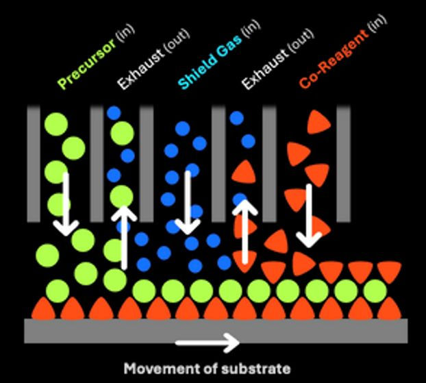
This approach translates the well-known ALD chemistry into a patternable format: instead of coating an entire wafer and then patterning, DALP deposits material only where needed, with features defined by the motion of the printhead. In other words, DALP is essentially maskless, localized ALD [4].
![Fig. 2: SEM Image of DALP® deposition of Atlant logo [4].](https://static.wixstatic.com/media/090711_5b664b705f3e431291f320d103ea2e78~mv2.jpg/v1/fill/w_976,h_294,al_c,q_80,enc_avif,quality_auto/090711_5b664b705f3e431291f320d103ea2e78~mv2.jpg)
2.2. ZnO Deposition with DALP®
ZnO deposition has been successfully demonstrated using DALP® process. In this approach, a safe and non-pyrophoric zinc precursor, bis(dimethylaminopropyl)zinc (Zn(DMP)₂), was used in combination with H₂O as the reactant, replacing the hazardous diethyl zinc (DEZ) typically employed in conventional atomic layer deposition (ALD) [5].
![Fig. 3: Optical micrograph of ZnO lines printed by DALP® at 200 °C using Zn(DMP)₂ + H₂O chemistry. Line thickness increases with the number of passes (50 – 800) [5].](https://static.wixstatic.com/media/090711_ea319a0b568c4756a7e6f80dd742f8b2~mv2.jpg/v1/fill/w_711,h_482,al_c,q_80,enc_avif,quality_auto/090711_ea319a0b568c4756a7e6f80dd742f8b2~mv2.jpg)

Comparing growth rate to traditional ALD, the DALP® ZnO process achieves a growth-per-pass (GPP) of approximately 1.1 Å/pass, nearly identical to the ~0.9 Å/cycle measured in traditional thermal ALD using the same precursor chemistry [5]. Both methods share the same self-limiting temperature window of 200-250 °C, within which stoichiometric and crystalline ZnO films are produced. This close alignment of growth kinetics demonstrates that DALP preserves the core benefits of ALD monolayer precision and reproducibility while adding the ability to pattern directly, greatly improving process flexibility and material utilization.
![Fig. 4: Comparison of ZnO growth rate between ALD (black) and DALP (red). Both exhibit a constant growth regime (ALD window) between 200–250 °C, yielding stoichiometric ZnO at ~1 Å per cycle/pass [5].](https://static.wixstatic.com/media/090711_d3db64a44dad4a00905e10383dac686c~mv2.jpg/v1/fill/w_624,h_517,al_c,q_80,enc_avif,quality_auto/090711_d3db64a44dad4a00905e10383dac686c~mv2.jpg)
To further validate the precision of the DALP® process, imaging ellipsometry was used to map the thickness profiles of ZnO lines deposited at 200 °C. The results demonstrate excellent uniformity along each printed line and well-defined edges, confirming that film growth remains consistent across the entire patterned area. The cross-sectional profile reveals a smooth, slightly rounded shape typical of self-limiting surface reactions, while the thickness maps for multiple lines show reproducible scaling with the number of passes. These observations underscore DALP’s ability to achieve highly uniform, conformal ZnO layers with nanometer-level accuracy, reinforcing its equivalence to conventional ALD in deposition control [5].
![Fig. 5: Thickness profiles and mapping of DALP-printed ZnO lines measured by imaging ellipsometry at 200 °C. (a) Cross-sectional thickness profile across a single line showing smooth curvature and uniformity; (b) thickness map of one printed line (~400 µm width); (c) set of ZnO lines with increasing numbers of passes (50–250), demonstrating reproducible, linear thickness scaling. Source: Stefanovic et al., 2023 [5].](https://static.wixstatic.com/media/090711_9369ead39242490989da9948b3ac0b04~mv2.jpg/v1/fill/w_915,h_287,al_c,q_80,enc_avif,quality_auto/090711_9369ead39242490989da9948b3ac0b04~mv2.jpg)
Comprehensive material characterization confirmed that ZnO films produced by the DALP® process are crystalline, stoichiometric, and free of defects, matching the high quality typically achieved by conventional ALD. Microscopic analyses using SEM and AFM revealed dense, homogeneous microstructures with nanoscale surface roughness and grain sizes of approximately 20-30 nm, which remained consistent across the tested temperature range. Grazing-incidence XRD measurements further identified the films as hexagonal wurtzite ZnO, exhibiting a pronounced (002) preferential orientation at around 250 °C, a texture particularly favorable for piezoelectric and electronic device applications. Complementary EDS and XPS analyses confirmed that ZnO layers deposited within the 200-250°C window are stoichiometric (Zn:O ≈ 1:1), while deviations at lower temperatures (150 °C) or higher temperatures (≥ 295 °C) resulted in oxygen-rich and zinc-rich compositions, respectively, attributed to incomplete surface reactions or precursor decomposition [5].
![Fig. 6: Microstructure of ZnO printed by DALP at different substrate temperatures (150 °C, 200 °C, 250 °C, 295 °C). SEM (top), AFM (middle), and XRD (bottom) confirm polycrystalline wurtzite ZnO with temperature-dependent orientation. Best crystallinity and stoichiometry occur near 200–250 °C [5].](https://static.wixstatic.com/media/090711_ba35427a9da2448793a033074cbfa504~mv2.jpg/v1/fill/w_918,h_484,al_c,q_85,enc_avif,quality_auto/090711_ba35427a9da2448793a033074cbfa504~mv2.jpg)
2.3. Further developments of ZnO using DALP® and Nanofabricator
At ATLANT 3D, we have also conducted extensive development and testing of ZnO deposition using the DALP® process, employing the same Zn(DMP)₂ + H₂O precursor-reactant combination as described in the literature. Our objective was to evaluate the electrical properties, specifically resistivity, of ZnO films grown under varying substrate temperatures and film thicknesses, to benchmark performance and identify optimization pathways. For electrical measurements, ZnO lines were printed on gold-padded wafers, which allowed for direct contact with predefined electrode pads and facilitated resistance testing. For resistance measurements we received help from the Danish Technological Institute (DTI) of these lines, as our in-house potentiostat was not sensitive enough for the task. The setup enabled accurate two-point resistivity measurements across multiple DALP® deposited ZnO lines of different thicknesses and deposition conditions.

Our measured ZnO resistivity-temperature curves are ≈3 orders of magnitude higher than the reference values and do not reproduce the characteristic trend reported in the literature. This discrepancy is most likely associated with the open-air deposition environment used in DALP® deposition. Literature indicates that ZnO grown in ambient conditions can exhibit increased resistivity due to oxygen adsorption and defect-related scattering at grain boundaries. A study by Ellmer & Mientus (2008) show that oxygen-rich surface states and grain boundary defects act as electron traps, thereby reducing carrier mobility in ZnO thin films deposited in non-inert atmospheres [6]. Similar behavior has been observed in open-air ALD systems, where uncontrolled oxygen incorporation leads to reduced conductivity compared to inert or vacuum processes.
![Fig 8: Left: Resistivity of DALP® deposited ZnO lines vs substrate temperature (600–1500 passes), showing a mid-temperature maximum followed by partial recovery at higher temperature. Right: Reference temperature dependence from literature for comparison (c) (highlighted).) [6].](https://static.wixstatic.com/media/090711_0c066e7f8fef413cb7448480a687a0d9~mv2.jpg/v1/fill/w_980,h_323,al_c,q_80,usm_0.66_1.00_0.01,enc_avif,quality_auto/090711_0c066e7f8fef413cb7448480a687a0d9~mv2.jpg)
Work is ongoing to further refine ZnO deposition conditions using DALP®. The lithography-free, direct-write nature of the technique allows for rapid, combinatorial optimization by systematically varying process parameters such as substrate temperature, deposition speed, gap distance between nozzle and substrate, and precursor and reactant bubbler temperatures. These tunable factors provide a wide process window to target improved crystallinity, stoichiometry, and electrical performance. Through systematic process mapping and controlled testing, DALP® continues to demonstrate its potential as a rapid prototyping platform for high-quality oxide semiconductors.

Positioning DALP® Within the ZnO Fabrication Landscape
Alternative Fabrication Methods for ZnO Thin FilmsBeyond DALP®, several fabrication routes have been proven to yield functional ZnO, each trading off precision, throughput, substrate compatibility, and post-processing. Among additive approaches, inkjet printing digitally patterns either nanoparticle dispersions or precursor inks that are converted to ZnO by thermal, UV, or plasma treatments. This enables maskless deposition on rigid or flexible substrates and large-area scalability, though film densification and crystallization typically require post-annealing and careful suppression of coffee-ring effects and porosity. Representative studies and reviews document successful thin films and devices prepared by inkjet, including recent demonstrations on flexible substrates and surveys of process-structure-property relations [7].
Two mature vacuum techniques pulsed laser deposition (PLD) and magnetron/RF sputtering remain benchmarks for dense, uniform ZnO. PLD can deliver highly stoichiometric and even epitaxial ZnO with excellent control of crystallinity via laser energy, oxygen ambience, and substrate temperature, albeit at limited area and higher system cost. Multiple studies and reviews outline PLD’s strength for high-quality ZnO thin films [8]. Magnetron/RF sputtering, by contrast, is industry-proven for large-area coatings at relatively low substrate temperatures; it provides dense, uniform layers suitable for transparent electronics, though patterning still requires masks or lithography and plasma exposure can introduce damage if not tuned [9].
Spray pyrolysis (including ultrasonic/nebulized variants) offers a low-cost, scalable path to ZnO by atomizing precursor solutions onto heated substrates, where thermal decomposition forms the oxide. It is attractive for rapid screening and large-area coatings but generally needs optimization to reduce roughness/porosity and to enhance film density and transport properties. Recent reviews and studies describe ZnO films produced by spray with controllable optical/electrical performance and post-treatments to improve crystallinity [10].
In summary, these methods map a practical spectrum of choices for ZnO: inkjet and spray routes offer low-cost, maskless patterning and rapid scale-up but typically rely on post-conversion to reach device-grade quality [6][9], while PLD and sputtering deliver dense, crystalline films with strong process control at the expense of vacuum infrastructure and added patterning steps [8][9]. DALP® complements this landscape by combining ALD-like, self-limiting growth with direct, lithography-free patterning using safer precursors, enabling fast design-to-device iteration and precise thickness control within the 100-300°C window, with far lower precursor consumption than blanket ALD [5].

Summary & Conclusions
This work outlined why ZnO remains a compelling platform material, combining a wide bandgap for optoelectronics with strong piezoelectric response for sensing and actuation, and showed that DALP® can deliver patterned, device-grade ZnO with ALD-like control. We reviewed literature results, detailed our own DALP-based ZnO growth, thickness uniformity, and microstructure, and discussed electrical measurements that highlight where open-air growth, contact geometry, and defect chemistry can shift resistivity trends. Taken together, the picture is clear: ZnO by DALP® retains the precision of ALD while removing lithography, making it a practical route for rapid, iterative device prototyping.
At ATLANT 3D, we are building on this foundation to expand ZnO capabilities in directions that matter for industry adoption: tighter control of stoichiometry and orientation within the 200-250 °C window; systematic de-embedding of contacts via TLM/four-point and Hall measurements; and process libraries that map substrate temperature, nozzle-substrate gap, stage speed, and precursor/reactant conditions to target electrical and piezoelectric figures of merit. The combination of DALP® with our NANOFABRICATOR™ Lite tool enables exactly this kind of rapid development, maskless, recipe-programmable, and combinatorial, so multiple thicknesses, chemistries, and device geometries can be explored on a single wafer in one run.

What to expect in Berlin?


Atomic layer processing is changing the way scientists and engineers develop high-precision materials. The method’s ability to create uniform zinc oxide coatings supports industries from solar energy to flexible displays. These processes rely heavily on precision, timing, and communication. Platforms like https://snapfish.pissedconsumer.com/customer-service.html remind us how vital it is for even digital creative tools to maintain accuracy. In both technology and art, precision defines long-term success.