


DP Patterning: How Dry Phase Patterning (DPP) is Revolutionizing the PCB Industry | Now Europe’s Largest Flexible Electronics Manufacturer?
- Apr 22
- 4 min read
Updated: Apr 30
Applications: Antennas · Electrodes · Conductors · Heaters · Circuit Boards
Conventional flex-PCB production is still dominated by wet chemical etching or printed conductive inks—processes built around multiple material steps, hazardous chemicals, and inherently unstable cost structures driven by silver and other volatile inputs. While widely adopted, these methods are increasingly misaligned with what the market now demands: scalable production, supply chain resilience, regulatory compliance, and verifiable sustainability.
Across industries, regulatory pressure is tightening. ESG (Environmental, Social and Governance) reporting requirements, restrictions on hazardous substances, and increasing scrutiny of chemical-intensive manufacturing processes are forcing companies to rethink not only what they produce, but how it is produced and documented. At the same time, geopolitical uncertainty and material volatility are exposing the fragility of globalized, chemistry-dependent supply chains.
DP Patterning’s patented Dry Phase Patterning (DPP) technology was developed to remove these constraints entirely.
At its core, DP Patterning replaces chemistry-based etching processes with a fully dry, mechanical roll-to-roll method. Instead of defining circuit geometry by selectively removing material through etchants and chemical processes, the pattern is formed directly in a metal-clad flexible substrate—typically aluminum-based laminates—using mechanical processing.
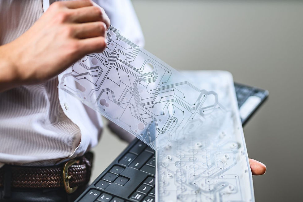
The process is based on two important steps to achieve well-defined structures:
First, a cliché is patterned with the desired geometry.
Second, a high-precision milling wheel removes only the protruded metal regions, leaving behind fully formed conductive traces on a flexible carrier.
The result is a continuous roll-to-roll production flow that converts raw laminate into finished flexible circuits without any wet chemistry, inks, or curing steps.
This has direct implications not only for performance and cost, but also for regulatory compliance and supply chain resilience.

Why DP Patterning is Outperforming Conventional Methods
Performance: Solid-metal conductivity instead of particle-based inks
Because DP Patterning uses solid aluminum and copper cladded aluminum (CCA)- foils rather than printed conductive inks, it delivers significantly higher and more stable electrical performance. Conductivity is typically 2–3× higher than printed electronics solutions, with improved long-term stability due to the absence of particle sintering or binder degradation.

Cost efficiency: Decoupling from material volatility and process complexity
By design, DP Patterning enables the use of widely available conductive materials and substrates such as aluminium-clad aluminium, and flexible carriers based on plastic or paper. This reduces dependence on silver-based inks and other high-cost, high-volatility materials, creating a more stable and predictable cost base.
In addition, the process eliminates multiple conventional manufacturing steps such as printing, drying, and sintering, thereby simplifying the overall production flow.
Simplicity and scalability: Fewer steps, higher industrial robustness
Traditional flex-PCB manufacturing relies on multi-step chemical sequences, each introducing variability, yield loss, and environmental burden. DP Patterning collapses this into a continuous mechanical process, significantly reducing process variability and enabling high-throughput roll-to-roll manufacturing suitable for industrial scale-up.

Sustainability & regulation readiness: Designed for a changing compliance landscape
Because DP Patterning is fully mechanical, it eliminates the need for etchants, solvents, and water-intensive processing. This directly reduces hazardous material handling, simplifies environmental reporting, and supports compliance with increasingly strict chemical and sustainability regulations in global manufacturing.
Material removed during patterning is generated as dry metal particles that can be recycled, avoiding liquid waste streams entirely. This is confirmed by an Independent Fraunhofer Institute Life Cycle Assessment (LCA), which reports up to ~98% reductions in CO₂, emissions and energy use compared to wet etching production - achieved through process step elimination rather than downstream compensation.
In a regulatory environment increasingly shaped by traceability, chemical restrictions, and ESG accountability, this represents a structurally compliant manufacturing model by design—not adaptation.
Supply chain resilience: From global dependency to local production
By removing reliance on complex chemical supply chains and volatile raw material inputs, DP Patterning enables a more robust and geographically flexible production model. Combined with roll-to-roll scalability and modular deployment, this supports localized manufacturing closer to end markets.
This reduces exposure to geopolitical disruption, shortens lead times, and increases control over critical production capacity—key requirements in an increasingly fragmented global supply environment.

From Process Innovation to Industrial Large-scale Production
Dry Phase Patterning introduces a fundamentally new approach to FLEX Electronics-manufacturing.
It represents a different process architecture —one that removes chemical processing entirely, reduces material cost volatility, and enables scalable production without sacrificing electrical performance.
In doing so, DP Patterning addresses a challenge the industry has faced for decades: how to achieve high performance, low cost, regulatory compliance, supply chain resilience, and real sustainability at the same time—without trade-offs.
This is what makes Dry Phase Patterning fundamentally different.
And why it is emerging as a new standard for flexible electronics manufacturing.
We look forward to discussing the technology and its applications in practice.
Visit DP Patterning at booth #E11.
We are exhibiting at
The Future of Electronics RESHAPED
in California, USA on 10-11 June 2026
Please register to meet us in person and see our technology in action.

Join the flagship TechBlick events in
California on 10-11 June 2026
This event is the global hub for Additive, Printed, Sustainable, Hybrid and 3D Electronics. It is where the global industry connects, where the latest is unveiled and where big products, novel ideas and key projects and partnerships are discussed and forged. This event is not to be missed!

This year, the event in California will also feature.


The event in Berlin will also feature:


Dry Phase Patterning (DPP) is truly shaking up the industry, and it’s about time we moved away from chemical-heavy etching! By utilizing mechanical precision, this method slashes waste and energy usage, proving that sustainable manufacturing can actually outperform traditional techniques. It’s exciting to see such a massive leap in flexible electronics. While new tech like this gains traction, finding a reliable PCBCool PCB manufacturer that stays ahead of these innovation curves is essential for any project. Whether you're chasing greener solutions or faster production cycles, embracing these advancements is the future. It’s definitely an inspiring time to be in electronics!