Heterogenous integration: Aggressive pitch scaling, Cu-Cu bonding, and transition to optical I/O
- Aug 26, 2022
- 2 min read
Heterogenous integration is the key to the future of computing. Here, the limiting factor is often the interconnect density (pitch) as well as bandwidth and energy consumption. Indeed, as we move towards platforms where multiple dies, potentially from different foundries, are all integrated into the same package, the issue becomes extremely important because die-to-die communication becomes the bottleneck.
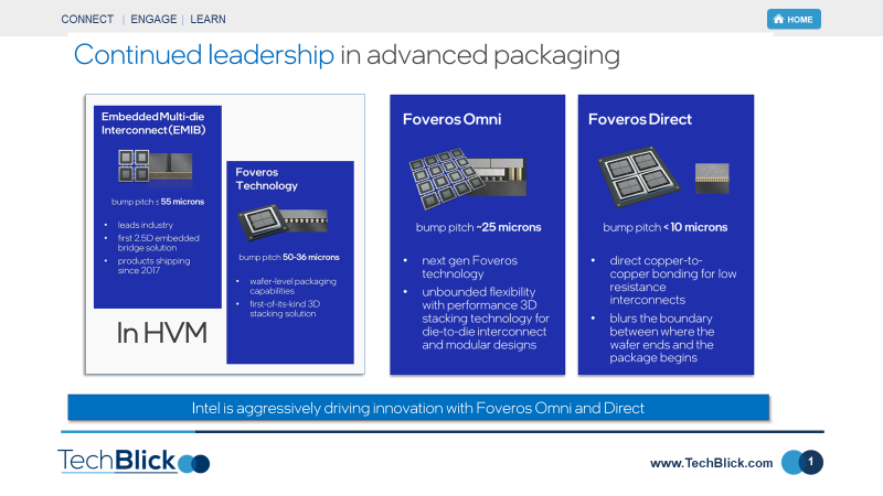
The first slide below are from Intel, presented at a conference in Sept 2021 online. Here, you can see the intended evolution of the technology. First, EMIB was launched. Here, a silicon bridge with <55um pitches serves as a small (2x2mm to 8x8mm) communication link between two separate dies in a package. This approaches is an alternative to the standard silicon interpose technology. Next was the development of Foveros platform, allowing face-to-face integration of dies from different foundries onto a package all connected via silicon base logic die. As you can see, these technology will involve with aggressive pitch scaling and a potential transition to direct Cu-to-Cu bonding from microbumps
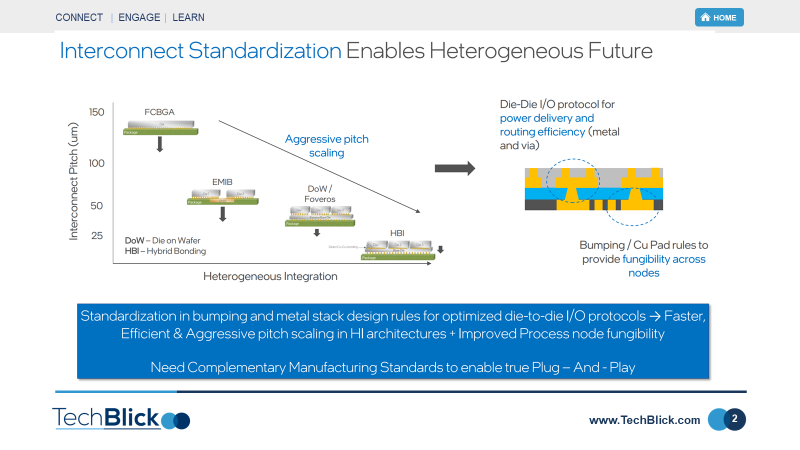
The second slide shows this trend further. It shows the evolution of interconnect pitch as heterogeneous integration advances. The common technology is flip chip BGA (FCBGA). The pitc here is limited to around >120um. Next, the EMIB was launched. Here, the pitch was reduced to 55um thanks to the silicon bridge technology. Now there is Fovereos which is based on die on wafer technology. The next generation will based on HBI or hybrid bonding
These heterogenous integration platforms can enable the integration of dies from different foundries. The challenge is though that each foundry has its own I/O designs, making ease compatibility difficult. It is helpful for the industry to develop common standards to enable a plug-and-play solution
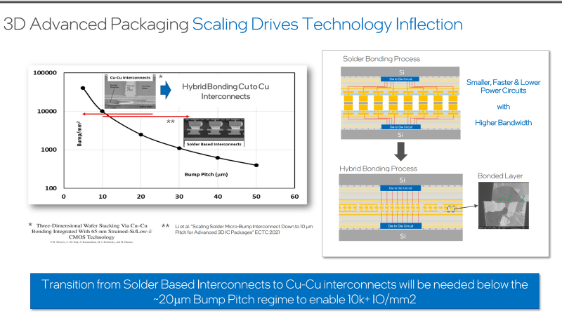
The third slide shows the need to transition towards Cu-Cu bonding. As the left chart shows, solder based microbumps can supported the technology until around 15-20um. Beyond this pitch level, a transition to Cu-Cu bonding becomes necessary. With this transition comes the possibility to increase bump density to over 10000/mm2. This is vital so that the I/O size and bandwidth do not limit overall system performance in complex multi-die packages.
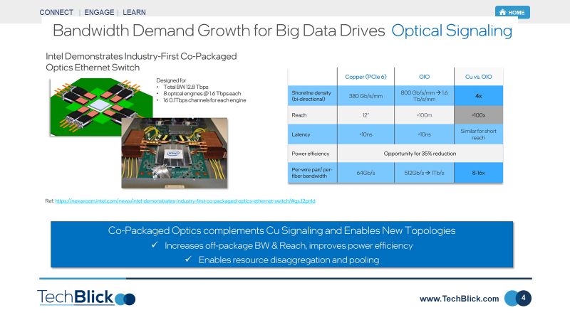
But will all suffice? The fourth slides show need to transition from Cu bonding to optical I/O technologies. As the comparison table shows, optical I/O (OIO) can increase shoreline density by a factor of4, reaching 1.6 Tb/s/mm. It will also improve power efficiency by some 35%.
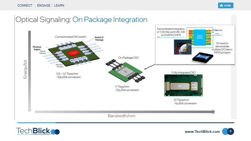
Finally, as shown in the fifth and final slide, this technology will need to evolve. The current (Sept 2021) demonstration was for an on-package OIO able to achieve >1Tpbs/mm @ 6 pJ/bit. The target is a fully integrated OIO able to achieve 10 Tbps/mm @ just 1pJ/bit conversation.
Heterogeneous integration is THE technology space to watch






Comments