


Hybridization or monolithic integration of GaN microLEDs on Si CMOS drivers: technology review
- Sep 29, 2022
- 1 min read
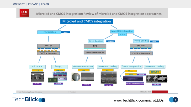
microLEDs can be directly integrated with CMOS drivers (instead of usual TFT backplane) enabling high-PPI displays suited to AR/MR glasses, metaverse, and even in some cases large-area displays. The key technological challenge for this is the hybridization and/or monolithic integration of GaN microleds and CMOS. This is no easy feat as it involves heterogenous hybridization or integration of two different material systems: GaN and Si.
Over the years, several technologies have been proposed by companies and institutions to hybridize the two parts. They are ranging from hybridization techniques to full monolithic 3D integration. These options – explored from over the last decade from 2011 to 2022- are depicted in the slide below, which offers a clear categorization of the techniques, e.g., hybridization vs monolithic integration, direct vs indirect bonding, align vs non-aligned, etc.
In this presentation, François Templier from CEA-Leti will review these techniques and explain challenges for their fabrication at TechBlick's specialist event on microLEDs on 30NOV-1Dec www.TechBlick.com/microLEDs . Some examples of solutions will be given, such as microtube technology and recent results with hybrid bonding.
More info www.TechBlick.com/microLEDs


Comments