


R2R Printed Electronics: Review of Application Space
- Dec 15, 2021
- 10 min read
Updated: Jan 20, 2022
Printed Electronics is everywhere and can be found in applications as diverse as a smart diaper to a precision missile. In this article, TechBlick will highlight some application and technology development cases for roll-to-roll (R2R) printed electronics.
In doing so, TechBlick will take you on a journey spanning applications in healthcare, automotive, photovoltaics, displays, and beyond. The common thread here is R2R printing of electronics regardless of printing technique, e.g., screen, flexo, gravure, slot die, etc. The applications reviewed herein are presented randomly and follow no particular order of importance. The images and examples below are extracted from 2021 presentations given at TechBlick, which is the home of printed, flexible, hybrid, and in-mould electronics.
TechBlick Individual Annual Pass or Group Access benefits for 12 months:
Events: Participate in all interactive LIVE (online) TechBlick events
Networking: Connect with the key players across the value chain from OEMs to material suppliers
Train: Learn the ins and outs of technologies from our portfolio of expert-led masterclasses
Market Assessment: Follow the latest market info and forecasts from leading market research analysts
Information Portal: Access the on-demand library of state-of-the-art fresh presentations
Discount: Major discount to participate in in-person physical events Printed, Flexible, Hybrid, and/or R2R Electronics | Additively Manufactured Electronics | Electronic Packaging | Quantum Dots | Micro- and Mini- LEDs | Printed and Flexible Displays | InMold Electronics | Fineline and Nanoimprinting | E-Textiles | Wearable Sensors | Intelligent Skin Patches | Graphene and 2D Materials | Carbon Nanotubes | Material Informatics | Solid State Batteries | InMold, Structural, and 3D Electronics | Perovskite, Organic, and Hybrid Photovoltaics | Battery Material Innovations
Medical sensors
Many sensors are printed. For example, glucose test strips are printed, often R2R. Given that they are a declining market thanks to rising of continuous glucose monitoring (CGM), we will not review them further here.
The image below shows two examples of R2R screen-printed sensors. The left image shows EKG electrodes R2R produced in large volumes, e.g., >1M/year units. The right image is an example of an incontinence sensor commercially R2R screen printed using conductive carbon on a stretchable non-woven material. It is an advancement of the art of functional R2R screen printing to be able to print using stretchable inks onto such thin and even stretchable substrates without creasing or improper stretching and without shrinking during the ink curing steps.

Source: Mekorprint
Rotary screen printing is also the basis of more advanced wearable medical sensors: smart skin patches. Below is a schematic of such product, involving rotary screen printing of stretchable conductive inks, dielectric inks, silver chloride inks, and beyond. These smart electronic skin patches are the basis of a wearable sensor platform enabling the measurement of vital signs. The patches can start with measuring heart rate and respiration and move on to other physiological parameters.

Source: Quad Industries
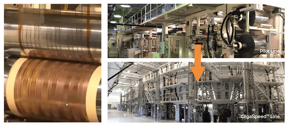
Another interesting recent commercial success story in R2R printed electronics is in a grade-I medical product developed by InnovationLab GmbH (iL) for Dr Jean Bausch GmbH & Co. KG: a digital articulating paper for digitally measuring the topography of teeth. These are 60μm thin sensors R2R printed on PI substrates using piezoresistive and silver inks, enabling digital measurement of 256 pressure levels.
The pilot R2R machine at iL can print five layers within one run and can print on a 33cm web with lengths up to 17m. Furthermore, the machine, shown below, integrates various curing (hot air, IR, UV, hot embossing) as well as converting (laminating, slitting, die& kiss cutting) modules. This machine can run up to 160 serial meters per minute (actual device not produced at this speed). The production machines, by iL's partners Heidelberger Druckmaschinen AG, can handle 44cm webs at much higher speeds thanks to a long, e.g., 25m, drying section.

Source: Innovation Lab GmbH and Dr. Jean Bausch GmbH & Co. KG presented at TechBlick 2021
Automotive
The next application I wish to highlight is in the automotive sector. A major trend in this industry is the replacement of mechanical switches with capacitive ones. The image below is from PolyIC GmbH (a Kurz company), showing an R2R printed transparent touch film integrated inside the driving wheel or gear of a vehicle. The transparent sensors are an R2R printed metal mesh film, consisting of 100nm thick silver nanoparticle inks printed with a line width and spacing of 10µm and 100 µm, respectively. The exact R2R printing technique is proprietary.

Source: PolyIC GmbH presented at TechBlick May 2021
Smart Packaging
The next highlighted application is in smart pharmaceutical packaging to improve medication adherence. Jones Healthcare Packaging has been actively developing this technology since 2013 and it is now in commercialization with real samples being tested by patients. The initial development was based on a narrow web pilot R2R printer (shown below) on a PET substrate using silver/carbon inks. The current product is flexographically printed using carbon inks on paper substrates. The printed carbon circuitry is shown below. This is of course the first generation of products. In the future, functional electronics, as well as printed displays, could be integrated into the smart packaging itself.

Source: Jones Healthcare presented at TechBlick March 2021
With the Annual Pass or Group/Company Access you can already access the following content from TechBlick 2021 events:
(9) Electronics Packaging Symposium: AI Chips, 5G Packaging, Chiplets. Heterogeneous Integration, High-Density Fan-Out Packages, Scaling, Future of Semiconductors
You can also see TechBlick’s growing portfolio of masterclasses
Photovoltaics
Now lets us switch focus to highlight R2R printed electronic applications in the photovoltaic industry. Organic photovoltaics has been in commercial development for 20 years or longer. Many may recall the heady days of Konarka (est. 2001), which went bankrupt in 2012 after having raised some $170M. Technology development continued without pause despite this setback. Now, both R2R printed and R2R evaporated approaches are reaching a high level of technology maturity. The example below is from Sunew in Brazil which have taken steps to scale up the production. The production line consists of 5 print stations, each station laying down one layer in the OPV stack. There are 32 print lines across the width of the web. The web width is 50cm and the length can be up to 1.5Km. Sunew can maintain thickness uniformity of <2% across the web width. Note that a major challenge in scale-up from lab results is the control of interlayer interfaces and the morphology of the donor-acceptor active layer. The left image shows how they can maintain a consistent efficiency as they go towards the 500mm web. The panel of images on the right show examples of actual installations of the R2R produced organic photovoltaic cells. Note that others such as Armor (R2R coating) and Heliatek (R2R evaporated tandem cell) are also scaling up the process in speed and width.

Source: Sunew (Presented in May 2021 at TechBlick conference)
Of course, many these days actively pursue perovskite photovoltaics (PePV), which have shown the fastest learning curve of all PV technologies. This technology can also be printed. For example, Energy Material Corp (EMC) is scaling up fully-inline unwind-to-wind R2R production of PePV. The right image below shows the ongoing transition from a pilot to a large-scale production line, highlighting the ambitious scale of the operation. The production line will involve R2R printing on 1.5m webs of 100µm thick flexible glass at web speeds approaching 30m/min. The ambition is to have an R2R printed PePV factory able to produce 20 million square meters per year.
The transparent conductive layer includes an R2R metal mesh layer printed using R2R flexography using Kodak technology. The metal mesh film shown below on the left is printed on 100µm Corning glass at 60m/min. The linewidths are not disclosed but the Kodak process can print sub-10 µm linewidths reliably at high web speeds.
Source: EMC (right) and Kodak (left).
Kodak image from a presentation at TechBlick (March 2021).
With the TechBlick Annual pass you can also participate in the following events in 2022:
(1) Battery Materials: Next-Gen & Beyond Lithium-Ion
(5) Micro- and mini-LEDs
(6) Quantum Dots: Material Innovations & Commercial Applications
(7) Graphene & 2D Materials: End Users, Applications, Major Producers & Start-Ups
(8) 5G/6G Materials
(9) Material Informatics
(10) Wearable Medical Sensors, E-Textiles, and Continuous Vital Signs Monitoring
Displays
R2R printing is also used to print electrochromic displays. This technology is not new but is now ready for mass production. The Ynvisible production line, based on R2R screen printing is shown below. The electrochromic display is multilayer consisting of a silver layer, counter electrode, electrolyte, symbol layer, electrochromic layer, and a graphic layer all sandwiched by a top and bottom moisture barrier substrate. To reduce production costs, converting and testing also take place inline R2R which is an important step forward. These printed electrochromic displays are suited for simple segmented displays targeted at high-volume IoT applications. The displays are <300µm thick and can be bent to a radius of 10mm. Furthermore, there is a very low power (1µW/cm2) as they can retain their state for 15min or longer before requiring a refresh. They can be powered at 1.5-3V and can be driven using simple microelectronics. This means that they could be powered by printed batteries and printed OPVs (see right image below showing such demonstrator). These displays can be attached to a target substrate using adhesives. In the latest developments, a graphical layer can also be added to give a sense of colour so the displays are on-brand.

Source: Ynvisible presented at TechBlick in July 2021
R2R printing is and can be used in other types of more complex displays. In quantum dot (QD)-LCD displays, the enhancement QD film is R2R slot die coated. An example is shown below on the right. This is a commercial success story. Printing may also play a role in the emerging microLED technology. It can be used to print wrap-around interconnects connecting the front side and backside of the glass substrate. It can also deposit bumps, connection pads, etc.
Early-stage development work is also underway to explore the possibility of some type of R2R process for placing the micro-LEDs themselves. Here, I highlight one early-stage approach based on the LIFT (laser-induced forward transfer) process followed by R2R rapid photo sintering on low-temperature substrates using standard solder.
In LIFT, a laser pulse is shone through a patterned transparent carrier. The laser hits a proprietary release coating, which releases the material or the component. The roadmap shown below on the left is by Holst Centre, showing how they first demonstrated, on a small-scale machine, narrow-line deposition of materials before progressing the technology towards component transfer. Recently, Holst demonstrated the use of LIFT to transfer 40x40x50 µm3 micro-LEDs with 80µm gap and 500µm interconnects. This lab-scale demo had a (relatively) low yield of 98% with 20% of LEDs ending up on their side. These results are far from production-ready, but they establish a roadmap with large improvement potential. This technique, when combined with R2R photo sintering, offers the chance to develop a fully R2R process.

Source: Right showing LIFT process by Holst Centre presented at TechBlick in June 2021. Left showing R2R slot die coated quantum dot enhancement film by Nanosys and partners.
There is tremendous progress in fineline R2R printing. The image below shows examples of work from Asahi Kasei in Japan. The company has developed a seamless roller mold (SRM) using electron beam lithography to achieve high-resolution seamless R2R imprinted films. Some results are also shown below, demonstrating the ultrafine feature capability of this R2R process. The application is close to commercialization, especially as a transparent RFID for track and trace.

Source: Asahi Kasei
R2R nanoimprinting can also be used to R2R create ultrafine features. The example below is hybrid R2R continuous process, developed by Printable Electronics Research Centre in Suzhou. The process enables the formation of ultrafine feature (<5µm) embedded metal mesh structures aimed at transparent touch and heating applications. The left schematic in the image below shows the process flow. Note that the embossing takes place using a rolling nano-embossing drum. The images in the middle show the metal mesh pattern and the embedded nature of the conductive lines, which enables one to thicken the line to achieve higher conductivity without compromising surface smoothness. The right image below shows an R2R machine that was previously deployed by O-Film to commercially R2R produce these metal mesh touch screens. At its peak, 1.5 million such panels were produced annually.

Source: Printable Electronics Research Centre in Suzhou presented at TechBlick March 2021
As a final topic to close our review, I would like to mention R2R RFID printing and how it is evolving towards R2R production of complex multi-chip hybrid circuits. In this case, I pick an example from Smooth & Sharp (S&S) in Taiwan which developed R2R printing on paper. In the simplest case, S&S began to R2R manufacture NFC on paper. These NFCs were at least 2x the price of their conventionally manufactured on-plastic counterparts two years ago. Now, S&S indicates that price parity is reached, which can help render more markets accessible.
Importantly, this is also the beginning of technical development. The NFC antennas have one small chip and a single metallization layer. As shown below, the future will be developing towards more chips, more layers, and more complicated circuit designs. The examples below show the integration of a 2-chip (NFC and LED chips) tag, the development of an 11-component piece (2 active layers and 10 passive components), and the demonstration of a 6-layer tag R2R printed on paper.
This is a very promising trend overall. The manufacturing facility for flexible hybrid electronics (FHE) is still in its relatively early stages of development but is advancing. Advanced ultrathin flexible chips, either natively flexible or thinned down, are becoming available. Currently, with the help of RDLs (re-distribution layers) these packages become capable with the resolution of printed lines on a flexible substrate. Importantly, low temperature attach techniques (photosintered solder, ultralow temperature solder, or particle-aligned conductive adhesives) are emerging to enable component to attach on PET and paper. This is the beginning of the roadmap towards R2R manufacturing of complex hybrid electronics.
In summary, we demonstrate that R2R printed electronics is really everyone with numerous applications. It is a vibrant and fast-evolving landscape. To learn more about this technology and ecosystem please refer to TechBlick (www.TechBlick.com). TechBlick is the home of printed, flexible, hybrid, 3D, in-mould, and 3D electronics worldwide.

Source: Smooth & Sharp presented at TechBlick May 2021
This seems like a simple prototype, but many technical challenges need to be overcome, especially as the surface is non-flat. In particular, the reliability of the components at interfaces (see below) needs to be tested and guaranteed. A major source of unreliability at these interfaces is the mismatch in the coefficient of thermal expansion of the different materials, which leads to stress build-up during thermal cycling. As shown in the table below, there is a wide range of coefficients involved.
A particular problem area can be the connection to the face-up dies. Here, aerosol deposits dielectric ramps upon which Ag tracks are aerosol printed. The conductive tracks can break, slip off, or disclose. Similarly, conductive tracks across areas filled with adhesive areas can also be a challenge. In this study, Parsons showcased its strategies to carry out reliability tests.
When you join TechBlick, you can hear and network with the following companies:

Comments