


The future of additive manufacturing – EHD printing technology redefines boundaries
- Apr 27
- 8 min read
Updated: Apr 28
The status quo of additive manufacturing and inkjet printing
How EHD technology is pushing the boundaries
EHD in practice – applications for industry
Implementation of EHD technology into the Notion Systems ecosystem The status quo of additive manufacturing and inkjet printing
Author: Simon Rihm | Notion Systems |https://www.linkedin.com/in/rihmsimon/
(1) The status quo of additive manufacturing and inkjet printing
Over the past two decades, additive manufacturing has undergone a profound transformation, evolving from a technology primarily confined to prototyping into a cornerstone of modern industrial production. This transformation is driven by its high flexibility, strong potential for customization, shorter development cycles, and efficient use of materials. By depositing material only where needed, additive processes significantly reduce waste compared to conventional methods - an advantage that is particularly important for expensive or scarce materials such as titanium alloys or high-purity metals. Additionally, additive manufacturing enables the production of complex structures that are difficult or impossible to achieve with traditional techniques, leading to lighter and higher-performance components.
The growing significance of additive manufacturing is especially evident in the electronics and semiconductor industries. These fields are defined by ongoing miniaturization, increasing integration density, and extremely stringent precision requirements. Conventional lithographic and mechanical fabrication methods are progressively approaching their technological limits, particularly in the context of flexible substrates, novel material systems, and cost-efficient large-area production. In this regard, additive technologies, most notably inkjet printing, offer decisive advantages and are becoming increasingly integrated into production processes worldwide.
From both an economic and technological perspective, it is becoming increasingly untenable to disregard the trend toward additive manufacturing. In most cases, the required investment amortizes rapidly, further reinforcing its attractiveness. It is therefore only a matter of time before additive manufacturing establishes itself as a dominant paradigm in industrial production.
(2) How EHD technology is pushing the boundaries
While inkjet printing is a well-established digital manufacturing technique, its inherent limitations - particularly in terms of feature size, ink viscosity, and adaptability to complex surfaces - restrict its use in advanced microscale research and semiconductor-grade applications.
Electrohydrodynamic (EHD) printing addresses these challenges by utilizing electrically driven jetting mechanisms. This approach enables the fabrication of structures in the single-digit micron range, supports a much wider range of ink viscosities, and operates entirely contactlessly. As a result, EHD printing allows precise patterning on non-planar and sensitive substrates, opening new possibilities in areas such as semiconductor packaging, heterogeneous integration, advanced interconnects, sensor technologies, and emerging nanoelectronic devices.
The key to these advantages lies in the fundamentally different droplet generation mechanism. In conventional inkjet systems, droplets are formed by pressure waves generated via piezoelectric actuation, which forces ink through a nozzle and inherently limits droplet size to the nozzle diameter while incurring energy losses due to fluid resistance. In contrast, EHD printing generates droplets through electric fields acting directly on the conductive liquid. This creates a balance between electrostatic forces and surface tension, forming a meniscus at the nozzle tip where energy is highly concentrated. Droplets are emitted from this localized region, allowing feature sizes significantly smaller than the nozzle diameter.
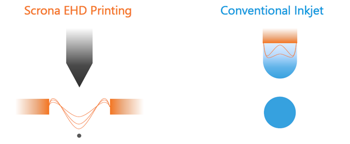
This alternative droplet generation mechanism offers several significant advantages. By decoupling droplet size from nozzle geometry, EHD printing substantially expands both the range of processable ink viscosities and the achievable resolution. While conventional inkjet systems typically produce feature sizes between 30 µm and 50 µm, EHD printing can achieve resolutions below 5 µm. At the same time, the viscosity window is greatly extended: whereas inkjet printing is generally limited to around 30 cP, EHD systems can handle viscosities exceeding 10,000 cP. However, such extreme conditions often require specialized printhead designs and may involve trade-offs in resolution, making it necessary to carefully balance viscosity and precision depending on the application.
Beyond droplet formation, the controlled transport of droplets is crucial for high-quality results. In EHD printing, electric fields are used not only to generate droplets but also to guide them with high precision. Unlike conventional methods that deposit material on predefined planar positions, EHD dynamically adapts to the substrate’s topography. This enables accurate patterning on curved, stepped, or otherwise irregular surfaces, significantly broadening the range of compatible geometries and allowing the fabrication of three-dimensional electronic structures and advanced packaging solutions.
Overall, this represents a substantial technological advancement over traditional inkjet processes, opening up new possibilities for manufacturing and functional integration.
(3) EHD in practice – applications for the industry
In practical applications, EHD printing is increasingly emerging as a key enabling technology across a wide range of disciplines. Its unique capability to combine ultra-high resolution, broad material compatibility, and precise, contactless deposition fundamentally expands the design space available to engineers and researchers. Unlike conventional manufacturing approaches, EHD does not merely optimize existing processes - it enables entirely new ones. This shift is particularly relevant in fields where established fabrication technologies are approaching physical, economic, or material-related limits. Against this backdrop, EHD printing acts as a technological catalyst, unlocking new degrees of freedom in device architecture, material integration, and system performance. The following application areas are intended to illustrate where the strengths of EHD technology lie.
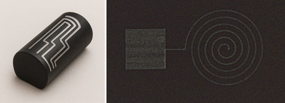
a. Enhanced topography printing
Topography printing enables precise material deposition on complex, non-flat surfaces and represents a key advantage of EHD-based processes. In particular, the MEMS-based printheads developed by Scrona ensure highly accurate and consistent droplet placement, even on curved, stepped, or irregular structures. This capability significantly surpasses conventional printing methods and opens new opportunities for the realization of three-dimensional electronics and advanced packaging solutions. Closely related to this is the concept of step printing, which allows controlled material deposition across discontinuities such as edges, gaps, or height variations on a substrate. This is particularly critical for applications in advanced packaging, conformal coatings, and optical structures. By enabling high-resolution, distortion-free printing over complex three-dimensional features, EHD technology avoids issues such as material overflow and loss of precision. As a result, it unlocks new degrees of design freedom and facilitates the development of increasingly sophisticated and integrated device architectures.

b. Novel display technologies

The rapid evolution of display technologies - driven by applications such as augmented reality (AR), virtual reality (VR), and next-generation consumer electronics - is placing unprecedented demands on resolution, brightness, and energy efficiency. Emerging concepts such as Micro-LED and Quantum Dot displays are widely regarded as key candidates to meet these requirements. However, their large-scale and cost-efficient manufacturing remains a significant challenge.
In this context EHD printing systems provide a fundamentally new approach to display fabrication. One of the central challenges in Micro-LED displays lies in the precise placement and patterning of color-converting materials, such as quantum dots, at extremely small pixel pitches. Conventional techniques - often relying on photolithography or transfer printing - face limitations in scalability, alignment accuracy, and material efficiency. EHD printing overcomes these barriers by enabling the direct, maskless deposition of quantum dot materials with sub-micron precision and highly controlled layer thickness. This capability allows for the fabrication of high-brightness, full-color microLED displays, where pixel density and optical performance are critical.

Beyond microLEDs, EHD technology also offers significant advantages for established display technologies such as OLED and LCD. By simplifying layer deposition processes and reducing reliance on complex masking steps, EHD can streamline manufacturing workflows, lower production costs, and enable more flexible design iterations.
c. Advanced semiconductor packaging
As the scaling of transistors in accordance with Moore's Law approaches both physical and economic limits, the semiconductor industry is undergoing a paradigm shift. Increasingly, performance gains are being achieved not through further miniaturization of individual transistors, but through innovations in system integration and packaging - an approach commonly referred to as “More than Moore”.
Advanced packaging techniques - such as heterogeneous integration, chiplet architectures, and 3D stacking - require new methods for interconnection, material deposition, and fine-structure fabrication. Traditional photolithographic processes, while highly precise, are often cost-intensive and inflexible when applied to these emerging architectures, particularly for non-planar or heterogeneous substrates.
EHD printing introduces a transformative alternative by enabling high-resolution, additive structuring directly onto wafers, chips, or package substrates. Its capabilities extend across a wide range of applications, including wafer and chip marking, solder bumping, via filling, and the direct patterning of redistribution layers (RDLs). The latter is especially significant, as RDLs are critical for routing electrical signals in advanced packages.
With its ability to achieve micrometer resolution and high aspect ratio structures, EHD printing is uniquely suited for fabricating dense interconnect architectures required in next-generation devices. Moreover, the digital, maskless nature of the process offers the potential to reduce fabrication costs by up to an order of magnitude compared to conventional photolithography, while simultaneously increasing design flexibility.
d. High-definition structures
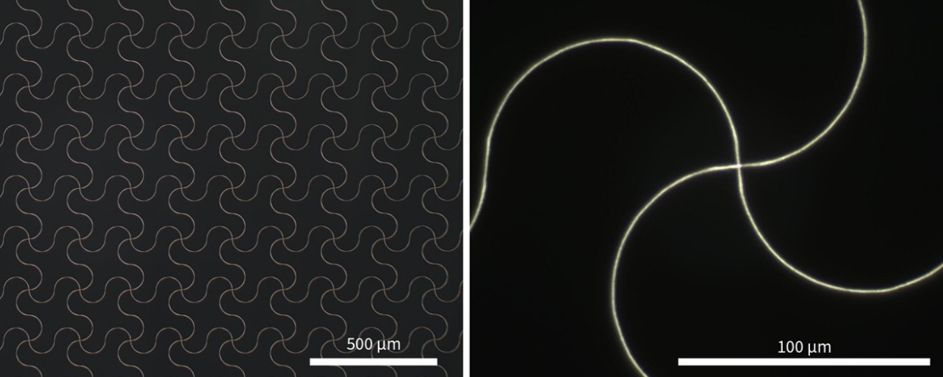
Antenna printing represents another important application of EHD-based additive manufacturing, enabling the precise deposition of conductive materials to form high-performance antenna structures. This is particularly relevant for devices such as consumer electronics, drones, and IoT components, where compact design and reliable signal transmission are essential.
EHD technology allows the fabrication of ultra-fine, low-loss antenna patterns on a wide range of substrates, significantly improving signal quality while supporting ongoing miniaturization. At the same time, it facilitates seamless integration of antennas into increasingly compact and complex electronic systems. As a result, EHD printing contributes to the development of highly efficient, space-saving communication components and expands the design possibilities for next-generation electronic devices.
(4) Implementation of EHD technology into the Notion Systems ecosystem
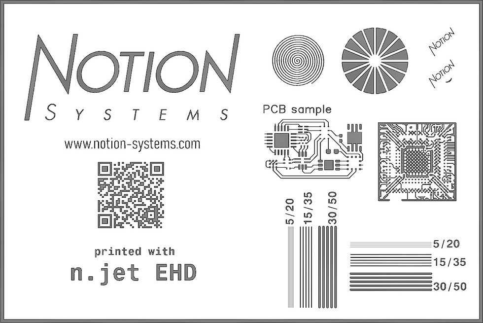
Through an exclusive collaboration, Notion Systems and Scrona have successfully translated advanced electrohydrodynamic printing into a user-friendly, high-precision research platform: the n.jet EHD. This partnership combines Notion Systems’ expertise in functional material printing systems with Scrona’s innovative multi-nozzle MEMS-based EHD printhead technology, aiming to accelerate the adoption of EHD printing in fields such as display technology, electronics manufacturing, and semiconductor production.
Within this framework, Notion Systems is responsible for manufacturing and servicing the n.jet EHD, which is specifically designed for advanced research and development applications. The system offers ultra-high precision and stability, including a printing resolution below 5 µm, repeat accuracy down to 1 µm, and a motion system with seven independently controlled axes. Additional features include an encoder resolution of 10 nm and support for substrates up to 150 × 150 mm. Mechanical stability is ensured through a granite base and vibration isolation, while integrated high-resolution top and bottom microscope systems enable precise alignment and real-time process monitoring.

As with conventional inkjet technologies, printheads play a decisive role in determining overall process performance. In the case of the n.jet EHD system, the latest generation of multi-nozzle MEMS printheads developed by Scrona (Gen3) significantly expands the operational capabilities available to the user. These printheads enable not only extremely high-resolution patterning but also the reliable processing of inks with elevated viscosities. Whereas traditional inkjet systems typically reach their functional limits at viscosities above approximately 50 cP, Scrona’s Gen3 printheads can handle viscosities of up to 300 cP while maintaining high print quality.
The advanced capabilities of the latest generation of EHD printheads are further reflected in a range of highly optimized technical features that enhance both process stability and application flexibility. Building on the multi-nozzle MEMS architecture, these systems are designed to meet the stringent requirements of high-resolution, high-performance additive manufacturing in research and industrial contexts.

The current generation of printheads is available starting from configurations with eight nozzles (Gen3-8), enabling parallelized material deposition and thereby increasing throughput without compromising precision. A key innovation lies in the implementation of nozzle-level ink circulation, which ensures consistent ink delivery, minimizes the risk of clogging, and contributes to overall process reliability - particularly when working with functional materials of higher viscosity. Thermal management is another critical aspect: integrated printhead heating of up to 75 °C allows precise control over ink rheology during operation. This capability is essential for stabilizing jetting behavior and expanding the range of compatible material systems.
We are exhibiting at
The Future of Electronics RESHAPED
in California, USA on 10-11 June 2026
Please register to meet us in person and see our technology in action.
Join the flagship TechBlick events in California on 10-11 June 2026
This event is the global hub for Additive, Printed, Sustainable, Hybrid and 3D Electronics. It is where the global industry connects, where the latest is unveiled and where big products, novel ideas and key projects and partnerships are discussed and forged. This event is not to be missed!

Comments