Search Results
1063 results found with an empty search
- Voltera: Dispensing Solder Paste on Factory Fabricated PCBs
Printed circuit boards (PCBs) are essential for electronic circuits, providing mechanical support and electrical connections for components. Factory fabricated (or sometimes called prefabricated) PCBs are pre-manufactured, ready-to-use boards that simplify assembly and ensure consistent quality in electronic devices. Contact: sales@voltera.io or +1 888-381-3332 ext: 1 Summary of Materials and Tools MATERIALS USED T4 Solder Paste Sn42Bi57.6Ag0.4 SUBSTRATES USED Factory fabricated PCB (FR4) TOOLS AND ACCESSORIES V-One PCB printer Tweezers Clamps Thumb screws Disposable nozzles Project Overview Purpose The purpose of this project was to demonstrate the feasibility of dispensing solder paste on factory fabricated PCBs precisely and reflowing the solder paste automatically. Design The board we selected for this project was a PCB used in the module hub of our NOVA material dispensing system . Since we designed the board in-house, we had the Gerber file for this project, which we uploaded into V-One’s software. Gerber file loaded into the V-One software Desired outcome The solder paste should be evenly dispensed on the designated spots of the FR4 board, with no overflow or voids. Once reflowed, the PCB should fit into the bottom of NOVA’s module hub. When connected to power, this board will allow NOVA to capture images of its work area. Front view of NOVA showing its module hub and work area Functionality The PCB contains a camera, LEDs, and other components that enable NOVA to capture images of the printed traces and pads, facilitating examination and ensuring optimal alignment. PCB mounted into NOVA’s module hub Preparing V-One The V-One software is intuitive and guides you through every step of the PCB prototyping process, including printing, soldering, heating, and drilling. Since the PCB was prefabricated, we didn’t need to print conductive traces or drill through holes. Instead, we followed the SOLDER workflow. The software prompted us to add the appropriate solder paste. We selected the T4 solder paste, and were then prompted to load a Gerber file. After loading the file, the software guided us through a quality check. Profile for T4 solder paste We cleaned the calibration switches using a few cotton swabs to remove any residual materials from previous use. Next, we clamped the PCB to the heated bed using four thumb screws and two clamps. After ensuring the PCB was securely fastened to the heated bed, we proceeded to probe the PCB. Probing the PCB To accurately dispense solder across the PCB surface, V-One first needed to generate a height map. We mounted the probe onto the carriage, and the software prompted us to align the features on the board with the features displayed in the software. This process was semi-automatic. Our task was to select reference points and adjust the probe's position using the software’s arrow controls. Once we were satisfied with the alignment, V-One began mapping the board's height. Probed points Dispensing solder paste on the PCB We inserted the solder paste into the dispenser slot, attached a disposable nozzle to the tip, and twisted the gear to prime the paste. Once there was a steady flow from the nozzle, we turned the gear back half a turn to slow down the flow and gently mounted the dispenser onto the carriage. Next, we selected the features we wanted to print in the software, and the dispenser moved to the designated positions to begin dispensing solder paste. Throughout the process, it was easy to adjust the paste flow by clicking the + and - buttons in the software. V-One dispensing solder paste on PCB Populating the PCB and reflow At this stage, the solder workflow was complete. We placed the components onto the board and selected HEAT > REFLOW > the T4 solder paste we used in the software. The heated bed started to heat the board automatically. The reflow process will last a few minutes where the solder paste is melted and cured, just like in a reflow oven. Once the board cooled down, we removed the board from V-one and our PCBA was completed. Choosing solder paste in software Advice for dispensing solder paste To ensure optimal performance, it is recommended to take the solder paste out of the refrigerator about 15 minutes before dispensing it onto the PCB. This acclimation period allows the paste to reach room temperature, improving its flow and consistency during application. Proper temperature adjustment helps prevent issues such as uneven dispensing or poor adhesion, which can result from changes in the paste's viscosity due to its thermal properties and temperature differences. Conclusion The board measures 100 mm × 83 mm. It took <7 minutes to complete the solder paste dispensing and about 24 minutes to complete the reflow step, which included heating up and cooldown time of V-One. After the reflow process, all the components were securely bonded to the PCB. When we attached the camera to the board and mounted it to the bottom of NOVA’s module hub, we were able to view the work area clearly in NOVA’s software. With precise control of the flow and flexible selection of features, V-One is an easy tool with intuitive processes for dispensing solder paste on factory fabricated PCBs. As we continue to explore the possibilities of solder paste dispensing, we invite you to view the other application projects we’ve completed. In the meantime, if you’d like to discuss your flexible PCB designs or our NOVA materials dispensing system, please book a meeting with our applications team or contact us at sales@voltera.io ! We are Exhibiting in Boston and in Berlin. Visit our booth at the TechBlick event on 11-12 June 2025 in Boston 22-23 October 2025 in Berlin
- Voltera: Printing a Flexible PCB with Silver Ink on PET
LED applications are popular engineering projects in school. Among these, an LED roulette stands out as it is intellectually challenging and fun. While a roulette circuit is typically printed on a substrate like FR4, printing on a flexible substrate presents further opportunities for education. Contact: sales@voltera.io or +1 888-381-3332 ext: 1 Summary of Materials and Tools MATERIALS USED Voltera Conductor 3 silver ink ACI Materials FS0142 Semi-Sintering Conductive Ink ACI Materials SI3104 Stretchable Printed Insulator Voltera T4 solder paste Voltera solder wire Siraya Tech Tenacious Flexible Resin SUBSTRATES USED Normandy Coating polyethylene terephthalate (PET) FR1 board TOOLS AND ACCESSORIES V-One PCB printer NOVA materials dispensing system Voltera disposable nozzle Nordson EFD 7018395 dispensing tip Nordson EFD 7018424 dispensing tip Nordson general purpose dispense tips NE555DR timer LEDs Project Overview Purpose The goal of this project was to prototype a flexible multilayer LED wheel roulette circuit that was traditionally considered rigid and validate the redesign of the circuit. Design This project involves a multilayer flexible PCB for the LED roulette circuit and a traditional control board that powers it. We adapted the design of an LED roulette circuit, originally developed for a 3” × 4” FR4 board by ITIZ , Voltera’s authorized reseller in Korea. This new version is printed on a coated biaxially oriented PET substrate, allowing the circuit to remain flexible — even when populated with components. Figure 1: Original LED roulette circuit design by ITIZ We divided the LED roulette circuit design into three layers: Base conductive layer Dielectric layer Top conductive layer Figure 2: Voltera modified design of the LED roulette circuit Desired outcome We anticipated the circuit would function like a roulette wheel: each time the pulse generator is triggered, the LEDs on the flexible PCB light up in a rapid circular sequence before slowing down and stopping on a single LED. Functionality By printing a dielectric and crossover layer on top of the base conductive layer, we created a compact and lightweight LED roulette circuit without using jumpers. Each layer remained flexible after curing, and the circuit maintained its integrity even after encapsulation and repeated flexing. When connected to power, pressing the switch on the control board caused the LEDs on the flexible PCB to light up, replicating the behavior of a roulette wheel as intended. Printing the control board This board controls the pulse signals and powers the LED roulette wheel circuit. We used V-One to print the circuit and reflow the components, which included: NE555DR timer LED Switch 47 µF capacitor 0.1 µF capacitor 10 nF capacitor 100 kΩ resistor 330 Ω resistor Figure 3: Schematic for the control board Figure 4: The control board Printing the flexible PCB This flexible PCB receives signals from the control board and lights up the LEDs as directed. Base conductive layer This layer consists of a roulette-shaped circuit (90 mm L × 70 mm W) that connects to the control board, as well as power and ground terminals, with designated gaps for dielectric pads. Figure 5: Schematic for the base conductive layer Figure 6: NOVA print settings, base conductive layer Figure 7: Print result, base conductive layer Dielectric layer This layer consists of 29 dielectric pads that provide insulation for the top conductive layer. For better coverage, we printed two passes of dielectric ink. Figure 8: Schematic for the dielectric layer Figure 9: NOVA print settings, dielectric layer Figure 10: Print result, dielectric layer Top conductive layer This layer consists of 29 fine crossover traces that connect the paths to the power terminal and control board. To address potential gaps over height changes, we decreased the trace width to 100 mm to enhance trace continuity. Figure 11: Schematic for the top conductive layer Figure 12: NOVA print settings, top conductive layer Figure 13: Print result, bottom conductive layer Post-processing the flexible PCB Dispensing solder paste and reflowing the components Once the circuit was cured, we dispensed solder paste using NOVA and populated the components before reflowing them in an oven. Figure 14: NOVA print settings, solder paste Figure 15: NOVA dispensing solder paste Because the wires are not heat-resistant, we manually soldered them onto both the companion board and the flexible roulette circuit. Encapsulating the components To reinforce their connection to the substrate, we dispensed encapsulation resin using a syringe onto the components and cured the resin in a UV light box. Figure 16: Encapsulated circuit being cured in a UV light box Once cured, we manually soldered the wires of the control board and the wires of the flexible roulette circuit together. Figure 17: Soldering the wires together Challenges and advice Electrical shorts We encountered issues with shorts due to multiple crossover lines on the dielectric layer. To address this, we recommend printing a second pass of the dielectric layer to achieve a thicker insulating layer that better supports additional layers printed on top. Drastic height changes A second pass of the dielectric layer can result in significant height differences. To handle this, it is advisable to set a low probe pitch to ensure a more accurate height map and print a thicker crossover layer for improved contact on the top layer. Maintaining flexibility with components attached To ensure the circuit remained flexible after populating components, we opted for smaller, more flexible components. This, combined with the use of a flexible substrate, encapsulant, and inks, allowed the circuit to bend without damaging the connections. Conclusion This project highlights the educational value of converting rigid circuit designs into flexible ones, allowing students to explore diverse materials and optimize print settings through experimentation. It also demonstrates the potential of prototyping flexible PCBs to replace electronics that were considered rigid, achieving lightweight, compact, and resilient designs. As flexible PCBs gain more popularity, hands-on experience with these technologies becomes essential for staying ahead in the rapidly evolving electronics industry. We invite you to explore our other projects as we continue to explore the possibilities of flexible PCBs and printed electronics. In the meantime, if you’d like to discuss your flexible PCB designs or our NOVA materials dispensing system, please book a meeting with our applications team or contact us at sales@voltera.io ! We are Exhibiting in Boston and in Berlin. Visit our booth at the TechBlick event on 11-12 June 2025 in Boston 22-23 October 2025 in Berlin
- Time to Book Your Place for 2025
TechBlick's Future of Electronics RESHAPED conference and exhibitions in 2024 were enormous successes with record participation. Thank you very much to all those who participated. And even though we are only at the start of 2025, our capacity is filling up fast at both our events. The Only Global Event On Additive Electronics, Printed Electronics, Hybrid Electronics, and Sustainable Electronics TechBlick is the only global offering in the field, combining onsite events in the USA and in Europe with an incredible online event series to reach the entire industry around the world. We had an incredible 2024 and are super excited about 2025. In Boston 2024 we had a sell-out event in the USA (Boston) bringing together the entire printed electronics industry. This event is now the largest and most important event in the field in North America. And we expect over 50% growth in 2025 vs. 2024. In Berlin 2024 we also had a fantastic and sell-out event. This remains our flagship event with a fully booked exhibition floor and over 550 participants. Our two online Innovation Festivals also continued to attract record participation with over 1600 registrants from right around the world Book Your Place NOW We strongly recommend that you book your place soon for 2025. Spots will be assigned on a first come first served basis. For Boston 2025, more booths than the entire 2024 exhibition are already booked. In fact, almost 80% of the expanded capacity is sold out. For Berlin 2025, nearly 65% of the capacity is already sold thanks to onsite re-bookings! USA | Boston, 11 & 12 June The Future of Electronics RESHAPED Conference and Exhibition USA Nearly 80% BOOKED already This is the largest and most important event in North America in our industry. You can find information about our packages and the latest floorplan here. We expect over 500 participants and over 75 exhibitors from around the world. Contact tom@TechBlick.com for more info and to book your place. Europe | Berlin, 22 & 23 OCT Future of Electronics RESHAPED Europe - The Most Important Printed Electronics SHOW 65% BOOKED Already This is our flagship event, each year with sell-out capacity. You can find information about our packages and the latest floorplan here. We expect around 80 exhibitors and 550-650 participants. Contact tom@TechBlick.com for more info and to book your place. Packages You can find the details of the packages here for Berlin and Boston. This year we are also offering GLOBAL packages, including USA + Europe + Online ✅ Onsite Exhibition: Berlin, Boston, or BOTH ✅ Onsite Talk: Depending on Your package ✅ Online talk at a conference of choice ✅ Year-round online booth at the TechBlick platform with 1200+ members ✅ Interactive live booth at online exhibitions - at our Summer Festival we had over 700 actual online participants! ✅ Email and social media marketing ✅ Leads and analytics ✅ 5 or more virtual annual passes offering access to all TechBlick online live events, library of more than 1300 talks, online networking events, online portfolio of masterclasses, and more. Contact tom@TechBlick.com for more info and to book your place.
- Break-through for novel red-emitting pyramidal microLEDs, based on the same InGaN material system as the green- and blue-emitting
Author: Oskar Fajerson , CEO, Polar Light Technologies With Polar Light Technologies’ novel concept, based on a non-etching bottom-up approach, red light at 625 nm has been achieved. By this remarkable breakthrough, Polar Light Technologies have reached red, green and blue pyramidal microLEDs employing the same material system. Polar Light Technologies has attained this milestone after more than 15 years research work and development. These novel microLEDs will open the gate towards future spatial computing and next-generation panel displays. The concept with the pyramidal design employed by Polar Light Technologies, will allow the ability with manufacturable microLEDs, while still maintaining their outstanding performance. Accordingly, the pyramidal microLEDs are ideal candidates for monolithic RGB displays. Red LED emission without compromises Due to the nitride material properties, there is an increasing challenge to realize efficient microLEDs as one goes towards longer wavelengths. While blue and green microLEDs have been on the market for years, reaching the red color is facing fundamental challenges due to the internal lattice-mismatch. Red color microLEDs have been demonstrated and reported, but they come with different compromises, such as manufacturability or the need to combine with other material systems. “Pursuing Polar Lights’ innovative pyramidal LED concept has been about overcoming those challenges without compromises. Today, thanks to a great tech team, we have succeeded in realizing the red-emitting microLEDs based on our innovative pyramidal structure”, says Lisa Rullik, CTO of Polar Light Technologies. High performance pyramidal LED structures Polar Light Technologies’ microLED technology is based on a bottom-up approach to form the LEDs of pyramidal design. This technology comes with unique benefits: A major challenge of the InGaN/GaN material system is the internal strain due to the lattice-mismatch, which can be better handled in PLTs pyramidal structures enabling manufacturing blue, green, and red microLEDs with the same material system, i.e. to build monolithic RGB. The pyramidal concept offers unique possibilities for hybridization between the frontplane and the backplane of the microLED. A major advantage of PLTs bottom-up concept is that the devastating etching is not needed, which means that the microLED performance can be maintained also as the dimensions of the LED structures are decreasing, since no etching damages will occur With PLTs pyramidal concept, it will be easier to integrate with CMOS and TFT A narrow output light cone (See Fig x): A Lambertian, or even sub-Lambertian, light lobe from the pyramidal emitter is important for many opto-applications e.g. micro-projectors These benefits are crucial for the microLED’ performance to solve key challenges for many applications and bring the Polar Light Technologies technology to the market. Next generation nanoLEDs Polar Light Technologies’ same-compound-based microLEDs offer high performance combined with excellent manufacturability. Their small dimensions and narrow emission cone further enhance the performance. The possibility to decrease the LED dimensions to the sub-mm regime will enable also the next LED generation – nanoLEDs: “Our technology addresses microLED challenges in a way that has never been done before,” says Oskar Fajerson, CEO of Polar Light Technologies. “Now we’re moving towards commercialization of this groundbreaking technology, focusing on putting products on the market.” About Polar Light Technologies Polar Light Technologies have developed a novel concept; a bottom-up approach to manufacture pyramidal microLEDs, atomic layer by atomic layer by MOCVD growth. In this way, the top-down destructive etching used for fabrication of micro-LEDs available on the market today can be eliminated. This will result is unmatched pixel size, emission brightness, light cone and energy efficiency. The company has its roots in manifold years unique research performed by Professor Per-Olof Holtz and his research team at Linköping University, with support from Vinnova, Sweden’s innovation agency and the Swedish Foundation for Strategic Research (SSF). For more information Oskar Fajerson, CEO of Polar Light Technologies Telephone: +46 738 19 38 00 oskar.fajerson@polar-light-technologies.com Lisa Rullik, CTO of Polar Light Technologies. Telephone: +46 760 21 34 80 lisa.rullik@polar-light-technologies.com Per-Olof Holtz, founder of Polar Light Technologies and professor at Linköping University Telephone: +46 708 75 26 28 per-olof.holtz@polar-light-technologies.com Do NOT miss the most important event of the year on MicroLED technology and AR/VR Display Technologies 🚀 Event: MicroLED Connect co-located with AR/VR Connect 📅 Date: 24-25 Sept 2025 📍 Location: Eindhoven, Netherlands https://www.microledconnect.com/ https://www.arvrconnect.com/
- Voltera: Printing ECG Electrodes with Biocompatible Gold Ink on TPU
Electrocardiogram (ECG) electrodes are sensors attached to the skin that detect the electrical activity of the heart. They are critical components of ECG systems used for diagnosis and management of cardiovascular diseases. This project demonstrates the process of printing a set of dry ECG electrodes. Project Overview Purpose The purpose of this project was to demonstrate how we validated the effectiveness of printing ECG electrodes on TPU ( Dupont Intexar TE-11C ) using biocompatible gold ink (Creative Materials EXP 2613-40) and stretchable silver ink ( Celanese Micromax™ Intexar™ PE874 ). We used the Voltera NOVA materials dispensing system and the Voltera V-One PCB printer for this purpose. Design We divided the project into three main parts: The ECG electrodes to be attached to the skin The control unit with the heart rate monitor and the controller An enclosure that protects the control unit from impact The SparkFun Heart Rate Monitor AD8232 (SENS-12650) acts as a pre-amplifier, transforming the heart’s biopotentials picked up by the ECG electrodes into a usable voltage while also rejecting electrical noise inherent in the measurement. The Arduino Micro captures the voltage and interprets it as a graph of the heart waveform through a program that we custom-made for this project. Figure 1: A graph showing beats per minute and ECG wave reading Desired outcome The printed electrodes should be flexible enough to conform to body movement and different physiques. Once the gold ECG electrodes are attached to the skin and connected to the circuit, we connect the circuit to power. The Arduino Micro controller should accurately interpret heart rates and rhythm readings. Functionality Inspired by this study where researchers developed a hexagonal labyrinth pattern as an optimized dry electrode geometry, this design allowed for maximum sensitivity while eliminating the need for wet gel, which can cause skin irritation in some patients. For this project we printed a set of three electrodes, to be placed on the chest, as a proof of concept. Although our design was able to output data into meaningful graphs, commercial ECGs typically have 12 points of readings. As such, this project is not intended for diagnosis or treatment of any medical conditions. Printing and post-processing the ECG electrodes To ensure the electrodes could conform to body movement and accommodate different physiques, we designed the corners to be stretchable. We divided the layout into two layers: Base silver layer for stretchability Top gold layer for biocompatibility Figure 2: Layer overview of the ECG electrodes This approach allowed us to use a relatively small amount of gold ink to minimize costs while achieving the desired outcome. Printing the base silver layer This layer consists of three circle patterns designed to connect to metal snaps, as well as traces that connect to the gold layer. For ease of alignment, we also included four sets of fiducials at each corner of the individual patterns. Figure 3: Silver layer design Figure 4: NOVA print settings for the silver layer Printing the top gold layer This layer consists of three hexagonal labyrinth patterns with traces that connect to the silver layer. Similar to the silver layer, we included four sets of fiducials for better alignment and precise cutting of the substrate. Figure 5: Gold layer design Figure 6: NOVA print settings for the gold layer Figure 7: Finished print of the electrodes Post-processing of the electrodes After the electrodes were printed, we punched a hole in the middle of the silver circle on each electrode for the metal snaps. Next, we folded the electrodes in the middle and inserted the metal snaps into the punched holes. Figure 8: One of the printed electrodes with a hole for a metal snap We cut three PET sheets proportional to the labyrinth pattern with the intention of inserting them between the layers of TPU. This added strength to the electrodes, preventing excessive stretching that could cause the gold ink to lose conductivity. We laminated them together using a T-shirt press machine. The electrodes were now ready to be connected to the heart rate monitor via the sensor cable. Figure 9: Laminating the two sides of the TPU together Printing the control unit To mount the Arduino Micro controller and the SparkFun Heart Rate Monitor, we needed to drill a few holes on an FR1 board using V-One. After drilling, we used V-One to print silver traces that electrically connected the two components together. Figure 10: FR1 mounting board design Figure 11: FR1 mounting board We then inserted rivets, mounted the components in place, and connected the wires from the heart rate monitor to the electrodes. Figure 12: FR1 board with components Printing the enclosure To protect the control unit from impact, we designed and 3D printed an enclosure that consists of a top and a bottom cover. Figure 13: Top cover of the enclosure Figure 14: Bottom cover of the enclosure After placing the control unit inside, we bolted the top and bottom covers together. Figure 15: Components and the enclosure Challenges and advice Minimizing material waste One of the primary challenges we encountered was managing the gold ink. Given its high cost, we aimed to avoid waste. To mitigate this risk, we initially experimented with alternative inks to validate the electrode design. We tested silver ink first to ensure successful prints before proceeding with the gold ink. We also included overlapping fiducial marks for the two layers in our design to ensure precise alignment. Optimizing ink flow The gold particles settled at the bottom due to being left unused for extended periods, which initially resulted in the nozzle clogging. We resolved this issue by mixing the gold ink using a dual asymmetric centrifugal mixer before printing. Conclusion While working with gold ink presented new challenges, using NOVA allowed us to precisely control the amount of ink dispensed, a benefit particularly relevant for applications using expensive materials. As we continue to explore the possibilities of bioelectronics, we invite you to view the other application projects we’ve completed. In the meantime, if you’d like to discuss your designs or our NOVA materials dispensing system, please book a meeting with our applications team or contact us at sales@voltera.io . We are exhibiting! Visit our booth C01 at the flagship TechBlick event in Berlin on 23-24 October 2024. Let's RESHAPE the Future of Electronics together, making it Additive, Sustainable, Flexible, Hybrid, Wearable, Structural, and 3D.
- ATLANT 3D: Transforming Advanced Manufacturing with Direct Atomic Layer Processing (DALP®)
In today’s world, semiconductor microdevices form the backbone of nearly every piece of modern technology. Manufacturing these tiny devices is a complex, multi-step process involving both additive (vapor deposition, sputtering) and subtractive (dry or wet etching) techniques. The key to success in this process is photolithography — a method that uses UV light to define patterns through specialized masks. But photolithography requires cleanrooms — highly controlled, particle-free environments. These facilities, marvels of engineering, are necessary to ensure contaminants don’t compromise device designs, but they come with significant costs and energy demands. Cleanrooms must operate with extreme precision, filtering the air to the highest standards and maintaining constant supplies of distilled water, pressurized gases like argon and nitrogen, and facilities to handle chemical waste. This intricate setup, while effective, is not only expensive but also energy-intensive, making it a significant bottleneck in manufacturing efficiency. The Promise (and Limitations) of Additive Manufacturing In recent years, additive manufacturing — more commonly known as 3D printing — has been heralded as a potential game-changer for many industries. From printing microscopic plastic parts to entire boats and even human tissue, additive manufacturing offers flexibility that traditional fabrication methods lack. However, for micro- and nanofabrication , 3D printing technologies like laser-based, electron beam-based, or inkjet methods face significant limitations. These methods typically achieve micrometer-scale resolution , which falls short of the nanometer-scale precision achieved by photolithography. Additionally, additive manufacturing has struggled to work with the wide range of materials — oxides, nitrides, metals, and complex compounds — used in semiconductor devices. Enter ATLANT 3D and Direct Atomic Layer Processing (DALP®) This is where ATLANT 3D comes in. By leveraging a novel approach called Direct Atomic Layer Processing (DALP®), ATLANT 3D is transforming the additive manufacturing landscape for micro- and nanofabrication. Figure 1: Illustration of the DALP® process; the printhead on top deposits gases onto a moving stage underneath DALP® combines the well-established technique of atomic layer deposition (ALD) with advanced mechatronics, using a microscale ALD reactor and a precision-moving stage (capable of X, Y, and Z-axis motion). This setup enables the selective deposition of materials, achieving nanoscale patterning and solving many of the challenges that have hampered traditional methods. DALP® offers direct, precise, and selective material deposition —one atomic layer at a time. The lateral feature size is determined by the microreactor, while the vertical feature size is controlled by the ALD process itself. This allows for highly controlled and repeatable patterning of materials like metals, oxides, and nitrides. Addressing Industry Challenges DALP® is uniquely positioned to address some of the most pressing challenges in advanced manufacturing: Precision and Efficiency : DALP® achieves direct patterning with incredible thickness accuracy, while minimizing energy use and process steps. Material Flexibility : Unlike traditional inkjet or screen printing, DALP® supports a wide range of materials, including oxides, nitrides, metals, and potentially all other materials that can be developed using the ALD method. Complex Geometries : Photolithography struggles with non-flat or corrugated surfaces. DALP® easily deposits materials on challenging geometries like 90 degrees wall of microchannels up to 60 µm deep , making it ideal for integrating functionalities such as sensors or functional coatings into microfluidic systems, for example. Cost and Sustainability : By reducing the need for multiple steps and minimizing material waste, DALP® offers a more cost-efficient and sustainable solution compared to traditional cleanroom-based methods. Rapid Prototyping : DALP® accelerates innovation cycles by allowing multiple depositions with different deposition parameters on a single sample. This speed enables quick iterations, making it easier to innovate and develop new devices. How DALP® Outperforms Traditional Methods DALP® outshines conventional additive manufacturing and photolithography processes in several key areas: Seed Layer for Metal Plating : Seed layer deposition using DALP® is very effective because it can quickly deposit the first very thin layers of a high-quality metal, which can then be used for metal plating – this speed is further emphasized by the direct patterning aspect, which removes the need for an additional lithography step. Catalysis and Electrocatalysis : [MC1] [SS2] [MC3] DALP® allows extreme control over surface morphology and porosity, increasing the active surface for increased catalysis activity. Moreover, DALP® can coat high aspect ratio substrates such as nano rods with active nanoparticles for higher catalytic yield. Direct Sensor Writing : DALP® can directly pattern a variety of materials used in sensing applications with atomic-layer thickness precision, simplifying the process and reducing the number of steps usually required in photolithography. Optical Filter Processing : DALP® deposits optical coatings on complex or non-flat surfaces, overcoming the uniformity challenges faced by other additive manufacturing technologies. Moreover, DALP® differentiates itself from traditional optics microfabrication most notably by its ability to easily deposit gradient structures, something that is costly with traditional additive & subtractive microfabrication processes. Seamless Integration and Complementary Capabilities DALP® can integrate seamlessly into standard cleanroom environments and works with established microfabrication processes. Rather than replacing traditional methods, DALP® enhances them by overcoming their limitations and offering greater flexibility. Figure 2: Deposited Pt across microchannels For instance, while photolithography is limited to flat surfaces, DALP® can pattern materials on non-flat, corrugated, or complex geometries. This opens up new possibilities in fields like MEMS, sensors, optics, and catalysis. DALP® in Action ATLANT 3D has demonstrated the power of DALP® through successful applications. As an example, we can show here the patterned deposition of platinum on a thermal silicon oxide wafer. More specifically, the control of the thickness is visible on the thickness mapping of the ATLANT logo, as expected for an ALD process the thickness is dependent on the number of passes. Figure 3: SEM picture of the ATLANT print Figure 4:Measured Pt thickness of the ATLANT print This process enables rapid material innovation and prototyping, reducing the number of iterations and materials needed for device development. The ability to deposit materials with such precision and selectivity, even on complex surfaces, makes DALP® a game-changer for industries looking to push the boundaries of what’s possible in micro- and nanofabrication. Conclusion ATLANT 3D's Direct Atomic Layer Processing (DALP®) technology is transforming the future of advanced manufacturing. By addressing industry challenges, integrating with existing processes, and offering unprecedented flexibility and precision, ATLANT 3D is redefining how we build the next generation of microdevices. For more information, visit atlant3d.com .
- Coherent | Real world data on LIFT transfer in MicroLED production
Author: Dr. Oliver Haupt, Director Strategic Marketing, Coherent, oliver.haupt@coherent.com Excimer-based laser-induced forward transfer (LIFT) is a practical mass transfer process for today and tomorrow. MicroLEDs stand at the forefront of next generation display technologies because they offer superior brightness, efficiency, and longevity over other panel types. In fact, the advantages of microLEDs are so significant that they promise transformative applications ranging from advanced smartwatches to expansive AR/VR experiences. However, the display industry faced a significant setback when tech giant Apple abandoned its ambitious microLED project after years of heavy investment (estimated at over US$3 billion since 2014). Apple hasn’t publicly announced their reasoning for this move. Those in the display industry who are not Apple suspect that they have not been able to develop a cost-competitive microLED display compared to existing OLED displays. They may not have utilized the latest advances in production technology to improve yield and throughput. A key to this could be the "mass transfer" process approach - a critical step in large-scale production. Here we’ll learn about the pivotal role of advanced mass transfer technologies and see how Excimer laser-based methods can overcome the production hurdles that might have stymied Apple. We’ll see how these offer a cost-effective and future-proof solution for microLED production. What Exactly Is “Mass Transfer?” We’ve described the process of mass transfer in some detail in past posts . Briefly, microLED production starts with the fabrication of red, green, and blue LEDs on separate substrates. These must ultimately be transferred to the final display circuit board. There they are arranged in groups of three (one red, one green, and one blue) to form each pixel of the display. In some cases, the LEDs are first moved from their original substrates to a “temporary carrier” where they are held on by adhesive. Then, they are transferred to the display panel. Other manufacturers move the LEDs directly from their original substrate to the display panel without an intermediate step. Either way, there are a couple of things that make mass transfer challenging. First, the LEDs must be placed with micron-level positional accuracy. Second, a very large number of LEDs must be transferred, so the process must be fast. For example, even just a 500x500 pixel display requires transferring 750,000 individual LEDs (500x500x3). Third, the process must be reliable to achieve the highest yield and avoid extensive repair. Plus, keep in mind, as microLED technology develops, the LEDs themselves will get smaller. Currently they’re about 50 x 50 µm, and they’re expected to eventually reach 10 x 10 µm or even beyond. The smaller the LEDs become, the more challenging it becomes to move them without damaging them, and to place them with the required accuracy. Lasers Lift Microleds To The Next Level Laser Induced Forward Transfer (LIFT) offers a practical, cost-effective means for mass transfer – both for current LED die sizes (about 20 µm x 20 µm) and moving forward towards smaller (10 µm x 10 µm) dies. In LIFT, pulses from an Excimer laser enter through the backside of the transparent temporary carrier. The light is absorbed in the buffer GaN layer and vaporizes it. This pushes the LED dies away and onto the display panel substrate, which is placed in close proximity. A final bonding step connects the LEDs to the panel substrate both mechanically and electrically. Excimer LIFT offers significant advantages over other mass transfer methods in the fabrication of microLED displays. One of the primary benefits is its high placement accuracy. LIFT can achieve placement precision below 1 µm, which is essential for the production of small, high-resolution displays. This level of accuracy ensures that each microLED is perfectly aligned, reducing the risk of defective pixels, which can compromise display quality. Moreover, the efficiency and speed of LIFT are unmatched. It allows for the transfer of millions of microLEDs rapidly and reliably, significantly reducing manufacturing time and thus, cost. This is particularly advantageous as display manufacturers aim to scale up production without sacrificing quality. Furthermore, the adaptability of laser-based mass transfer to different substrates and microLED sizes offers flexibility. This versatility is crucial as the demand for diverse types of microLED applications grows, ranging from tiny wearable devices to large-scale ultra-high-definition televisions. Additionally, our LIFT solution is designed to be future-proof. As the microLED market evolves to utilize even smaller LEDs with tighter pixel pitches, excimer LIFT systems can quickly adapt. This can be accomplished without extensive retooling or downtime, ensuring that manufacturers can stay ahead in a competitive market. This adaptability, combined with the Coherent commitment to ongoing research and development, positions our solution as a pivotal technology for the future of displays. Real-World Results Coherent applications engineers recently performed testing to quantify some of the parameters for implementing LIFT with microLED dies substantially smaller and thinner than any devices currently in production. Specifically, we tested the placement accuracy of LIFT with 5 µm x 5 µm x 3 µm (thickness) microLEDs as a function of gap distance (distance from the temporary carrier holding the microLEDs to the target substrate). This data is useful because very small gap distances (below 50 µm) are hard to reliably maintain in a volume production environment. So, LIFT must be capable of working quickly, reliably, and at scale over larger gaps than this, even with small LED dies. The experimental setup used a Coherent UVtransfer to move microLEDs from a 4-inch GaN donor wafer to a 100 mm diameter quartz recipient wafer. Placement accuracy (in x and y) was measured with a microscope and machine vision system that could automatically identify the dies and determine the center position of each. For each gap distance, 979 microLEDs were moved. The graphs show placement accuracy (offset from the ideal position) for all 979 of the microLEDs, with a 50 µm gap and die-to-die pitch of 90 µm. To summarize this data, 99.7% (3σ) of the microLEDs were placed within 0.66 µm (x) and 0.56 µm of their of their target location. Position offsets for LIFT of 979 microLEDs measuring 5x5x3 μm³ each, transferred over a 50 µm gap and with a die-to-die pitch of 90 µm. The next graph shows how placement accuracy varied with gap distance. Submicron placement accuracy was maintained at gap distances of up to 80 µm. These numbers show that LIFT is entirely practical with these small microLEDs. Mean 3σ position offset deviation (average of X and Y 3σ values) as a function of transfer gap distance for LIFT of 979 microLEDs with dimensions of 5x5x3 μm³. MicroLED displays offer a revolutionary viewing experience, but mass production hurdles have held back their deployment and discouraged even some of the most technically savvy manufacturers. Excimer laser-based LIFT overcomes one major production hurdle and succeeds where other mass transfer technologies have failed. It enables precise, high-speed transfer of even the smallest LEDs, and is based on lasers that have demonstrated 24/7 operational reliability in other demanding display fabrication processes. Plus, the adaptability of LIFT ensures compatibility with ongoing microLED advancements, making it a future-proof solution for display manufacturers and paving the way for commercialization of this technology. Learn more about LIFT. Coherent | MicroLED Processing Advanced Laser Solutions
- Advances in Printed Electronics: From FHE Integration to Sustainable Manufacturing and Cutting-Edge Printing Technologies
In this newsletter, you’ll learn about advancements in additive manufacturing, flexible electronics, sustainable electronics manufacturing, printed electronics, and microfabrication. You will also have the opportunity to download the full presentation slides. DoMicro | Insights in Electronic Design and Integration For FHE-Application Hummink | Pushing The Boundaries of Microbump Fabrication: The HPCaP Approach Elephantech | Making the world sustainable with new manufacturing technologies NanoPrintek | Dry Multimaterial Printing: Printed Electronics WITHOUT Inks or Drying Fuji Corporation | Innovation in electronics by integration of additive manufacturing and SMT The Future of Electronics RESHAPED Boston is the flagship TechBlick event. This event will take place at the UMass Boston, USA on the 11-12 June 2025. Visit the event website here. ** The EARLY BIRD Rates expires on 20 Dec 2025. Please book now https://www.techblick.com/registration https://www.techblick.com/ DoMicro | Insights in Electronic Design and Integration For FHE-Application Marcel Grooten | April 2024 In this presentation you will learn about the following: Conventional and flexible hybrid electronics Creating flexible hybrid electronics In-house electronics test lab: electronic development competence in quality management tools, electronics development tools and in-house electronics test lab Product & prototyping Download the Full Presentation Slides Here Hummink | Pushing The Boundaries of Microbump Fabrication: The HPCaP Approach Sahar Al Kamand | April 2024 High aspect ratio microbumps are vital in packaging applications, yet typical methods lack the control needed for dimension. HPCAP (High Precision Capillary Printing) Technology addresses this, offering high control over microbump fabrication & exceptional versatility in dimensions & materials. Based on Atomic Force Microscopy (AFM) , HPCAP simplifies complex microbump manufacturing into a single-step procedure. During this presentation, we will delve into the workings of HPCAP technology. Our aim is to provide a detailed exploration of how this groundbreaking technology facilitates the creation of microbumps. Furthermore, the presentation will underscore the vital role that HPCAP technology plays in both packaging and semiconductor repair applications. In this presentation you will learn the following: The working principle of HPCaP The macro resonator Capillarity is the only driving force Adding a new dimension to printing Gaps at the submicron scaleunmatched precision & accuracy in EHD, Inkjet, UPD, HPCaP Common sense physical boundaries in rheology & drying, particle size, surface energy Download the Full Presentation Slides Here Elephantech | Making the world sustainable with new manufacturing technologies Masaaki Sugimoto | March 2024 In this presentation you will learn the following: Pure Additive Method: A novel approach using metal inkjet printing for electronics. PCB Industry Impact: Why the subtractive process is wasteful and its environmental costs. Sustainable Solutions: Cost-effective methods for greener PCB manufacturing. Mass Production Breakthrough: The first mass production plant for inkjet-printed PCBs in Aichi, Japan. Download the Full Presentation Slides Here Join us on December 11, 2024, for the FREE-TO-ATTTEND Printed Electronics & Display Innovation Day , a free online event by TechBlick and the MicroLED Association. Connect with industry leaders shaping the future of displays. View the agenda here . https://www.techblick.com/ NanoPrintek | Dry Multimaterial Printing: Printed Electronics WITHOUT Inks or Drying Masoud Mahjouri-Samani | April 2024 In this presentation, you will learn about a flexible method to integrate advanced materials and devices onto various objects Challenges with Current AME Printers: Issues like complex supply chains, costly ink formulations, and sustainability problems. A Comprehensive Solution: Learn about a dry multi-material printer that consolidates the entire supply chain and manufacturing process into one machine. Advanced Imaging Techniques: Insights from scanning transmission electron microscopy (STEM) of laser-generated nanoparticles. Adhesion Testing : Results of adhesion tests for ANM-printed silver (Ag) films. Impact of Sintering: Understanding how laser power density and printing passes affect substrate integrity and reduce paper burning. Download the Full Presentation Slides Here Fuji Corporation | Innovation in electronics by integration of additive manufacturing and SMT Ryojiro Tominaga | Berlin 2023 In recent years, 3D printer technology that can manufacture bare PCBs using digital printing technology for both conductors and insulators has been developed. However, it is essential to optimize the SMT process in accordance with the transformation of the bare PCBs manufacturing process for the practical application of this technology. Fuji will introduce a novel machine that combines the additive manufacturing process of bare PCBs and low-temperature SMT technology optimized for this purpose. In this presentation, you will learn about Low temperature SMT and Fast and smooth data flow Integrated machine of AME + SMT AME capability establishment of specific SMT process suites for AME Target interconnect structure and Ultra low temperature SMT process Direct flow from designing to manufacturing Fast testing cycles utilizing FPM-Trinity and the data flow Download the Full Presentation Slides Here Join us on December 11, 2024, for the FREE-TO-ATTTEND Printed Electronics & Display Innovation Day , a free online event by TechBlick and the MicroLED Association. Connect with industry leaders shaping the future of displays. View the agenda here .
- Carbon Nanomembranes for Metal Anodes, Solid-State Battery Materials Testing, Sodium-Ion Batteries, and Roll-to-Roll Manufacturing Innovations
This issue of the TechBlick newsletter highlights battery technology, featuring insights from industry experts. Albert Schnieders from CNM Technologies discusses how Carbon Nanomembranes (CNMs) are enabling metal anode batteries by preventing dendrite growth and improving performance with standard separators. Dr. Christoffer Karlsson from rhd Instruments covers the improvements in solid-state battery materials testing through active pressure and temperature control. Rene Windiks from Materials Design explores atomic-scale modeling to optimize battery materials and enhance performance and safety. Marja Vilkman from VTT introduces the SOLiD EU project, focused on sustainable manufacturing and Roll-to-Roll (R2R) processes for solid-state batteries. Lastly, Shmuel De-Leon examines the growing sodium-ion battery market, its advantages and limitations, and the future of mass production. CNM Technologies | Enabling metal anode batteries by modifying the anode & separator interfaces with Carbon Nanomembranes rhd Instruments | Improving Solid State Battery Materials Testing through Active Pressure and Temperature Control Materials Design | Advancing Battery Materials Through Atomic Scale Modeling VTT | The development of R2R processes for manufacturing solid state batteries. The newly launched SOLID EU project Shmuel De-Leon | Sodium Ion (Na- Ion) Battery Market 2024. The Next Technology on Battery Mass Production Register by end of December and save 150 Euros! Use discount code: Save150EurosSSB CNM Technologies | Enabling metal anode batteries by modifying the anode & separator interfaces with Carbon Nanomembranes Albert Schnieders | 2023 To overcome the limitations of lithium-ion batteries, new battery technologies, such as lithium and beyond lithium metal, are being investigated. However, these solutions often suffer from dendrite growth or surface passivation at the metal anode site. Carbon nanomembranes (CNMs) are an electrically insulting 2D nanomaterial that has shown its ability to conduct lithium ions and promote homogeneous ion deposition when used in conjunction with conventional separators. These properties open the possibility of using CNMs as a promising material to enable metal anodes batteries, not only by modifying the interface of separators but also of metal anodes by acting as an artificial solid electrolyte interface to prevent dendrite growth. We will discuss in this presentation the technical and economic potential of these possibilities of CNMs in next-generation batteries. Explore the following in this session: The transition to metal anode batteries and the challenges of excessive dendrite growth. How Carbon Nanomembranes (CNMs) can prevent dendrite build-up in metal batteries. The high potential of CNMs when combined with standard separators in metal-based battery tests. Download the Full Slides Here rhd Instruments | Improving Solid State Battery Materials Testing through Active Pressure and Temperature Control Dr Christoffer Karlsson | 2024 Key takeaways from this session include: Solid electrolyte conductivity - How to achieve reproducibility Pelletization (fabrication) pressure Measurement pressure & Measurement temperature Active materials - Three-electrode full cell testing – Example of NMC/graphite with Li reference electrode Download the Full Slides Here Materials Design | Advancing Battery Materials Through Atomic Scale Modeling Rene Windiks | 2024 Topics covered in this session include : Industry Challenges: Rapid need for low cost, enduring concepts for high energy batteries while maintaining rigorous safety requirements R&D Strategies necessitate a comprehensive understanding and control of the material’s properties and behavior during battery operation The Value of Modeling: Multi-scale simulations insights and data where experiments are costly and time-consuming Collaborative Approach: Materials Design is developing a multi-scale modeling approach together with industrial and academic partners Case Studies: Prediction of thermophysical properties of polymer composites and time evolution of microstructure at metal electrode/solid electrolyte interface Download the Full Slides Here Join us on February 11-12, 2024, for the Solid-State Battery Materials , a virtual event by TechBlick. Engage with industry leaders driving innovation in battery technology. Explore the agenda here. Register by end of December and save 150 Euros! Use discount code: Save150EurosSSB Register Now TechBlick.Com VTT | The development of R2R processes for manufacturing solid state batteries. The newly launched SOLID EU project Marja Vilkman | 2023 In this session, you will learn about : Sustainable batteries The SOLiD project: Sustainable manufacturing and optimized materials and interfaces for lithium metal batteries with digital quality control R2R manufacturing of solid-state batteries - NMC811 cathode + interfaces - Polymer electrolyte - Li anode + interfaces - Quality control - Life cycle analysis and exploitation Download the Full Slides Here Shmuel De-Leon | Sodium Ion (Na- Ion) Battery Market 2024. The Next Technology on Battery Mass Production Shmuel De-Leon | 2024 This session is about - Sodium Ion Batteries are the next large production capacity technology for the rechargeable battery arena. Our presentation will review technology advantages/ limitations – and the motivation beyond bringing that technology to the market. Last year around 10 companies in China start production of different cell formats – Cylindrical, Prismatic and pouch. Will review some of the market players status and our prediction for the future Sodium Ion Battery Market. Download the Full Slides Here Join us for TechBlick’s Fourth Online Event: Explore the future of battery technology and discover the latest advancements in the battery industry, with key topics including: Solid state batteries Beyond Li batteries including sodium, metal-air, tin, aluminium, etc Next-generation anodes, cathode, and electrolyte materials Additive and/or dry manufacturing methods Register by end of December and save 150 Euros! Use discount code: Save150EurosSSB Book Now
- World's First System for Testing AR Contact Lenses
Authors: [1] Dr. Kedar Sathaye , Product Manager Light & Display at Konica Minolta Sensing Europe B.V. [2] Dr. Valentyn Volkov , co-founder of XPANCEO The market for image display devices is rapidly evolving, with innovations ranging from advanced screen technologies in smartphones and TVs to more sophisticated solutions like augmented reality (AR) glasses and virtual reality (VR) headsets, such as the Apple Vision Pro. The XR market alone is projected to reach an impressive $1,913.7 billion by 2032, with a growth rate of 39.2% from 2024 to 2032. There’s an increasing focus on making these devices more wearable and user-friendly. Achieving this goal, however, presents significant challenges due to the limitations of current technologies. Wearable devices, particularly in the AR and VR sectors, often face critical performance issues. For example, AR glasses and VR headsets frequently lack sufficient brightness, have limited battery life, and often end up being bulky due to the need for larger batteries. These issues can lead to overheating and reduced field of view, decreasing the practicality of these devices for long-term use. This is driving the industry to innovate and develop new devices that overcome these challenges. However, this rapid development invites another problem: the lack of comprehensive test solutions to ensure that these new devices meet the required standards for quality, safety, and performance. In response to this gap, Konica Minolta and XPANCEO have partnered to meet the growing demand for contemporary test solutions. AR Smart Contact Lenses XPANCEO is a deep-tech company pioneering smart contact lenses, a new frontier in wearable technology that it envisions as the next generation of computing. These lenses aim to solve the problems of current wearable technology by integrating various traditional device functions into a single interface that is weightless and as natural to the wearer as their own vision. Beyond applications such as health monitoring and enhanced vision, a key focus for XPANCEO is image projection. The company has already succeeded in developing a smart contact lens with a display that significantly outperforms standard solutions. By reducing the resolution in the peripheral vision area—where the eye does not require high resolution—the load on the video controller is minimized, allowing for much smaller packaging. Additionally, the brightness loss from the display to the eye is reduced threefold, and the total power consumption is expected to be only 1-3 µW, which is 100-300 times less than comparable AR glasses. However, this technological advancement raises new questions about testing and quality assurance, as there are currently no ready-to-go solutions on the market. Image projected by XPANCEO lens Image Quality Testing To help manufacturers like XPANCEO ensure quality of the display, Radiant’s AR/VR Lens paired with a ProMetric® Imaging Photometer or Colorimeter provides unique optics engineered for measuring near eye displays (NEDs), such as those integrated into virtual, mixed, and augmented reality headsets. The innovative new geometry of the lens design simulates the size, position, and binocular field of view of the human eye. Unlike traditional lenses where the aperture is located inside the lens, the aperture of the AR/VR Lens is located on the front of the lens to enable the connected imaging system to replicate the location of the human eye in an AR/VR device headset and capture the entire FOV available to the user. Radiant developed an AR/VR Lens to address the unique challenges of qualifying integrated NEDs under the same conditions as they are visualized by human users. The AR/VR Lens is designed to be paired with high-resolution imaging photometers and colorimeters, 16-megapixel and higher resolutions. By capturing displays at this detail, the measurement system can evaluate the entire display FOV at once with the precision to capture any defects that might be noticeable to the human eye. The Radiant AR/VR Display Test Solution includes (left to right): AR/VR Lens, ProMetric® Imaging Colorimeter or Photometer, and TrueTest™ Software with optional TT-ARVR™ module. Radiant’s AR/VR display test solution is specially designed for in-headset display measurement. What separates the AR/VR Lens from other optical components is the lens’s ability to replicate the FOV and entrance pupil of human vision. The AR/VR Lens product specifications include: Aperture (entrance pupil) located at the front of the lens. 3.6 mm aperture size. The average pupil will contract to 1.5 mm in diameter in bright light and dilate to 8 mm in diameter in darkness. Radiant uses 3.6 mm for two reasons: 1) it is in the mid-range of pupil dilation; 2) the 3.6 mm aperture allows a high MTF for the lens. Wide FOV to 120° (±60°) horizontal. Importance of Calibration Each Radiant AR/VR camera/lens system is factory calibrated to ensure the most accurate images for absolute light and color analysis. Calibration processes include factory distortion calibration to remove lensing effects of the wide-FOV lens, ensuring accurate spatial analysis of the display by the camera software. When measuring displays using a wide-FOV lens, the image captured by the lens may appear distorted as shown in figure below. Top, an image captured by an uncalibrated wide-FOV system; bottom, image captured by a system with distortion calibration applied. Because the AR/VR solution uses a fisheye lens, an uncalibrated image exhibits barrel distortion. Radiant’s camera/lens solution is calibrated to process out distortion effects before applying display tests. This ensures accuracy of spatial measurements to detect defects where they occur on the display. Software Solution Radiant TrueTest™ Automated Visual Inspection Software applies analyses to all images captured by Radiant’s AR/VR measurement solution. This platform includes a suite of display tests with standard tests for luminance, chromaticity, contrast, uniformity, and defects like dead pixels and lines. In addition, unique tests for AR/VR projections are available in the pre-configured TT-ARVR™ software module. Some examples of TT-ARVR software analyses are shown in Figures 14-16 below. These analyses are performed on the AR/VR display to test the manufacturing specifications of the AR/VR device. These specifications can also be published for consumer use (for instance, on an AR/VR headset specification sheet) to help them evaluate the device and compare with competitive products. Uniformity analysis as shown in figure below determines areas of low or high luminance across the display, which may indicate a defect in the display. This analysis can also be used to characterize the uniformity against design specifications. Uniformity analysis (shown in false color) characterizes display quality. A checkerboard contrast analysis as shown in figure below is performed by projecting a checkerboard pattern on the display within the AR/VR headset. Once the pattern is imaged by the AR/VR test system, the checkerboard contrast test evaluates luminance levels in the image to determine the display system’s ability to project distinct light and dark values - a performance parameter that can be indicated on a specification sheet. Checkerboard contrast analysis evaluates the contrast ratio of the display. Customized Testing Radiant Vision Systems, a Konica Minolta Company that focuses on solutions that can be used across various applications, has partnered with XPANCEO to develop a custom testing system that measures critical parameters for these emerging devices: Field of View: The XR smart contact lens is designed to allow users to see images from any angle, requiring precise measurements to ensure the gradual improvement of this parameter. Brightness of Virtual Images: While traditional light bulbs can be easily quantified, virtual images provide a subjective experience that necessitates an objective testing system. This is particularly important given strict medical guidelines on image brightness to prevent damage to the human eye. Contrast: This measures how clearly an image stands out from the background and is crucial for comfortable and safe viewing. It should remain stable regardless of the brightness of the environment. Adaptation to Weather Conditions: The brightness of virtual images needs to adjust to different weather conditions, similar to how phone screens adapt, without causing excessive brightness that could blind the user if they look directly at the sun. The gradient of Intensity Across the Field: For optical reasons, virtual images have varying brightness, especially at the edges. Accurate measurement of this parameter is essential for correcting the image when it’s recorded for projection. Line Sharpness: This parameter ensures that fine lines and details in the image are clear and easy for the user to see. The testing system assembled in XPANCEO lab These advancements in testing are not only applicable to smart contact lenses but could revolutionize quality assurance in a variety of fields. Though the fully realized smart lens is still in the research and development stage, the technology behind it holds promise for broader applications in the industry, offering a significant opportunity for further development and standardization in wearable tech testing.
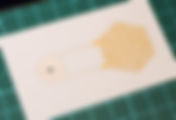
- Voltera: Printing Electroluminescent Ink on Paper and PET
As presented at the recent TechBlick’s Future of Electronics RESHAPED USA event held in Boston, our project, Multilayer Flexible Displays Using Electroluminescent Ink , validated the use of the Voltera NOVA material dispensing system to print a multilayer electroluminescent display on PET and paper using various Saralon inks. In this article, we explain how this project was achieved, covering the inks and substrates used, the steps we followed, as well as challenges and tips on printing flexible multilayer projects using the direct-ink-write technology. Contact: sales@voltera.io or +1 888-381-3332 ext: 1 Summary of Materials and Tools MATERIALS USED Saralon Saral Silver 700 Silver-Based Conductive Ink Saralon Saral Dielectric 600 Dielectric Ink Saralon Saral BluePhosphorl 800 Electroluminescent Ink Saralon Saral Conducting Polymer 700 Polymer Electrochromic Ink SUBSTRATES USED Polyethylene terephthalate (PET) Cardstock paper TOOLS AND ACCESSORIES Nordson EFD 7018424 dispensing tip Nordson EFD 7018333 dispensing tip Nordson EFD 7018482 chamfered tip Adafruit 12V EL wire/tape inverter Project Overview Purpose The purpose of this project was to demonstrate the multilayer capability of Voltera NOVA . We printed a blue light-emitting pattern - the Voltera logo - on two substrates: paper and PET separately, using electroluminescent ink. Design layout Electroluminescence operates by exciting a phosphor material with an electric field. An inverter is needed to convert the direct current from the power source into alternating current. Based on this mechanism, our design positioned a phosphor layer between two conductive layers, incorporating a dielectric ink layer to insulate the phosphor. The printing sequence was as follows: Layer 1: Base conductive layer Layer 2: Dielectric layer Layer 3: Phosphor layer Layer 4: Top conductive layer Desired outcome Once connected to an alternating current (140 V, 1.862 kHz), the phosphor layer should emit blue light, illuminating the Voltera logo with an even glow across both prints. Functionality We determined the Voltera logo would be suitable for this project. It is feasible to incorporate designs into larger electronic applications, including billboards, branded merchandise, and control panels. Printing the electroluminescent Voltera logo Base conductive layer (1) This layer consists of a Voltera logo pattern (55.5 mm L × 19.75 mm W) and positive and negative traces that connect to power and ground terminals. Print settings on NOVA software (1) Result on paper (left) and on PET (right) (1) Dielectric layer (2) This layer features a dielectric Voltera logo pattern which measures 23 mm L × 15 mm W and two dielectric pads. These extra pads help ensure the top conductive layer is appropriately insulated. Print settings on NOVA software ( 2) Result on paper (left) and on PET (right) (2) Phosphor layer (3) This layer contains a Voltera logo pattern, slightly smaller than the dielectric layer (by 0.5 mm each way), printed with blue light-emitting ink. Print settings on NOVA software (3) Result on paper (left) and on PET (right) (3) Top conductive layer (4) Lastly, this layer includes a conductive overlay with an opening at the bottom left to prevent short-circuiting. It measures 29.5 mm L × 21.5 mm W and connects to the ground terminal. Print settings on NOVA software Result on paper (left) and on PET (right) (4) Challenges and advice for printing multilayer electroluminescent displays Trapped air Air bubbles can form in inks that have been left unused for an extended period. These bubbles caused the dielectric layer to break when we cured it in the oven. Mixing the ink with a dual asymmetric centrifugal mixer before printing will eliminate air bubbles. Additionally, it is recommended to allow the dielectric layer to dry naturally at room temperature instead of curing it in an oven. Uneven glow During our experiments, some prints exhibited dark areas, leading to an uneven glow. This issue can arise from several factors: The top conductive layer being too thick The phosphor layer being too thin or getting scratched off during dispensing of the ink for the top conductive layer Irregularities in print height Adding fiducials to each layer helps improve alignment and print quality. In terms of print settings, if the layer is too thick, increasing the print speed, reducing the height (we reduced it to approximately 40 µm), and using a smaller nozzle can be helpful. If the layer is too thin, try to reduce the print speed. Furthermore, in multilayer projects, changes in height can happen drastically when printing over existing traces. Setting a low probe pitch will make the height map more accurate, ensuring the height transition at the edges of features is accurate and reducing the risk of traces being printed off-course. Conclusion The paper substrate provided consistent results throughout our experimentation, due to its absorbent nature. Each layer was smoother on paper than on PET, highlighting the potential of using paper as a substrate in EL display applications. On the other hand, PET, being flexible and chemically resistant, offers the advantage of suitability for more demanding use cases. As demonstrated by this project, with careful attention and fine-tuning of the print settings, the results of EL display on PET are equally impressive. Electroluminescent logo final print EL displays are also intriguing when printed on glass and other non-conductive substrates. As we continue to explore the possibilities of electroluminescent displays, we invite you to view the other application projects we’ve completed using NOVA and V-One. In the meantime, if you’d like to discuss your designs or our NOVA materials dispensing system, please contact us at sales@voltera.io . We are Exhibiting in Berlin. Visit ou r booth at the TechBlick event on 23-24 October 2024 in Berlin.