Search Results
Search this site
1084 results found with an empty search
- A bioelectronic tongue ‘tastes’ sweetness
Candy, cookies, juices. Just about everyone likes sweet treats, but what one person thinks tastes too sugary, another might think is just right. This variability makes it challenging to develop new foods and beverages, so companies have sought a more objective method. Now, researchers reporting in ACS Applied Materials & Interfaces have developed an ultrasensitive bioelectronic tongue that measures sweetness by mimicking human taste buds. Although human sensory panels are the most common way to analyze a substance’s taste, there can be a lot of differences in how people perceive flavors. To get more objective data, researchers have made bioelectronic tongues in the lab, but they either are complicated to manufacture or can’t fully replicate the way the human tongue works. Human tongues have sweet taste receptors with two large, complex structures that bind to compounds such as sugars. The outermost portion of one of these structures is called the Venus flytrap domain because its hinged, two-lobed molecular structure resembles the leaves of the insectivorous plant that close around its prey. This domain interacts with most of the sweet substances a person consumes. In a previous study, Tai Hyun Park, Seunghun Hong, and colleagues made an umami sensor with a human-like performance by using just the protein at the end of the umami taste receptor. So, these researchers wanted to apply the same concept to make a sweet-sensing bioelectronic tongue, using the Venus flytrap domain as electronic taste buds. The researchers attached copies of the Venus flytrap domain that were made by bacteria in a thin layer on a gold electrode. They then connected multiple gold electrodes together with carbon nanotubes, making a field-effect transistor device. When solutions of naturally sweet sucrose or of the artificial sweetener saccharin were applied to the device, the current decreased. The sensor responded to these solutions down to the 0.1 femtomolar level, which is 10 million times more sensitive than previous bioelectronic sweet sensors, the researchers say. The device could also consistently measure the sweetness of real drinks, such as apple juice and sucrose-sweetened chamomile tea, but it did not show a response when cellobiose (a tasteless sugar) or monosodium glutamate (a salt known as MSG) were introduced. Because the bioelectronic tongue was both sensitive and selective for sweet-tasting compounds, the researchers say this could be a powerful tool for the health care, pharmaceutical, and food and drink industries. The authors acknowledge funding from the National Research Foundation (NRF) of Korea, the Ministry of Science and ICT (MSIT) of Korea, the Ministry of Trade, Industry and Energy (MOTIE) of Korea, Samsung Electronics, the European Research Council (ERC) within the European Union’s Horizon 2020 programme, and the Korea Institute of Science and Technology (KIST) Institutional Program. More info: https://www.acs.org/content/acs/en/pressroom/presspacs/2022/acs-presspac-january-26-2022/bioelectronic-tongue-tastes-sweetness.html
- Tiny battery-free devices float in the wind like dandelion seeds
Wireless sensors can monitor how temperature, humidity, or other environmental conditions vary across large swaths of land, such as farms or forests. These tools could provide unique insights for a variety of applications, including digital agriculture and monitoring climate change. One problem, however, is that it is currently time-consuming and expensive to physically place hundreds of sensors across a large area. Inspired by how dandelions use the wind to distribute their seeds, a University of Washington team has developed a tiny sensor-carrying device that can be blown by the wind as it tumbles toward the ground. This system is about 30 times as heavy as a 1-milligram dandelion seed but can still travel up to 100 meters in a moderate breeze, about the length of a football field, from where it was released by a drone. Once on the ground, the device, which can hold at least four sensors, uses solar panels to power its onboard electronics and can share sensor data up to 60 meters away. The team published these results in Nature. “We show that you can use off-the-shelf components to create tiny things. Our prototype suggests that you could use a drone to release thousands of these devices in a single drop. They’ll all be carried by the wind a little differently, and basically, you can create a 1,000-device network with this one drop,” said senior author Shyam Gollakota, a UW professor in the Paul G. Allen School of Computer Science & Engineering. “This is amazing and transformational for the field of deploying sensors because right now it could take months to manually deploy this many sensors.” Because the devices have electronics on board, it’s challenging to make the whole system as light as an actual dandelion seed. The first step was to develop a shape that would allow the system to take its time falling to the ground so that it could be tossed around by a breeze. The researchers tested 75 designs to determine what would lead to the smallest “terminal velocity,” or the maximum speed a device would have as it fell through the air. “The way dandelion seed structures work is that they have a central point and these little bristles sticking out to slow down their fall. We took a 2D projection of that to create the base design for our structures,” said lead author Vikram Iyer, a UW assistant professor in the Allen School. “As we added weight, our bristles started to bend inwards. We added a ring structure to make it stiffer and take up more area to help slow it down.” To keep things light, the team used solar panels instead of a heavy battery to power the electronics. The devices landed with the solar panels facing upright 95% of the time. Their shape and structure allow them to flip over and fall in a consistently upright orientation similar to a dandelion seed. Without a battery, however, the system can’t store a charge, which means that after the sun goes down, the sensors stop working. And then when the sun comes up the next morning, the system needs a bit of energy to get started. “The challenge is that most chips will draw slightly more power for a short time when you first turn them on,” Iyer said. “They’ll check to make sure everything is working properly before they start executing the code that you wrote. This happens when you turn on your phone or your laptop, too, but of course, they have a battery.” The team designed the electronics to include a capacitor, a device that can store some charge overnight. “Then we’ve got this little circuit that will measure how much energy we’ve stored up and, once the sun is up and there is more energy coming in, it will trigger the rest of the system to turn on because it senses that it’s above some threshold,” Iyer said. These devices use backscatter, a method that involves sending information by reflecting transmitted signals, to wirelessly send sensor data back to the researchers. Devices carrying sensors — measuring temperature, humidity, pressure, and light — sent data until sunset when they turned off. Data collection resumed when the devices turned themselves back on the next morning. To measure how far the devices would travel in the wind, the researchers dropped them from different heights, either by hand or by drone on campus. One trick to spread out the devices from a single drop point, the researchers said, is to vary their shapes slightly so they are carried by the breeze differently. “This is mimicking biology, where variation is actually a feature, rather than a bug,” said co-author Thomas Daniel, a UW professor of biology. “Plants can’t guarantee that where they grew up this year is going to be good next year, so they have some seeds that can travel farther away to hedge their bets.” Another benefit of the battery-free system is that there’s nothing on this device that will run out of juice — the device will keep going until it physically breaks down. One drawback to this is that electronics will be scattered across the ecosystem of interest. The researchers are studying how to make these systems more biodegradable. “This is just the first step, which is why it’s so exciting,” Iyer said. “There are so many other directions we can take now — such as developing larger-scale deployments, creating devices that can change shape as they fall, or even adding some more mobility so that the devices can move around once they are on the ground to get closer to an area we’re curious about.” Hans Gaensbauer, who completed this research as a UW undergraduate majoring in electrical and computer engineering and is now an engineer at Gridware, is also a co-author. This research was funded by the Moore Inventor Fellow award, the National Science Foundation, and a grant from the U.S. Air Force Office of Scientific Research. More info: https://www.washington.edu/news/2022/03/16/battery-free-devices-float-in-wind-like-dandelion-seeds/
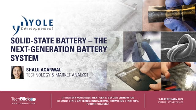
- Solid-state battery – the next-generation battery system
Speaker: Shalu Agarwal | Company: Yole | Date: 9-10 Feb 2022 | Full Presentation Li-ion batteries have become the primary technology of choice for many applications in the consumer electronics industry and empowered the electric vehicle (EV). However, the flammable liquid electrolyte of Li-ion battery is responsible for safety issues, such as electrolyte leakage, fire, or explosion. In addition, the demand for higher energy density, fast charging capability, lower cost, and safer EVs has recently created a resurgence of interest in solid-state batteries. In its talk, Yole Développement will present the advantages of solid-state batteries over conventional Li-ion batteries as well as the challenges associated with their development, like low ionic conductivity, poor wettability of solid electrolytes, high operating temperature, etc. Solid-state battery manufacturers must achieve battery production processes that are scalable and compatible with existing lithium-ion production technology to remain successful in the overfilled market. Bringing solid-state technology to mass production is a difficult task. Therefore, partnerships are more important than ever to get all the necessary solid-state battery know-how together: technology, equipment, high-volume / high-yield production, and end-systems. Today, many batteries and automotive manufacturers have presented their target roadmaps for mass production to secure a leadership role in the solid-state battery market despite the remaining technology and supply chain challenges. The solid-state battery is considered the ultimate battery technology for next-generation battery systems. Based on the achievement of technology milestones and growing supply chain collaborations, Yole Développement expects that solid-state battery commercialization will start in about 2025. However, small-scale production may happen even earlier. The intensive development efforts of EV/HEV makers and their partners will result in a progressive adoption of the solid-state battery as a “premium” battery in the 2025-2030 period. After further optimization and production scaling, solid-state batteries will spread to other applications, but their high added value will remain mainly in e-mobility applications. Yole Dévelopment will analyze the key success factors for mass production of solid-state batteries. Join TechBlick on an annual pass to join all live online conference or online version of onsite conference access library of on-demand talks (600 talks + PDFs) portfolio of expert led masterclass year-round platform https://www.techblick.com/ Our next battery-related event will take place on 15-16 FEB 2023, covering 1) Solid-State Batteries: Innovations, Promising Start-Ups, & Future Roadmap 2) Battery Materials: Next-Generation & Beyond Lithium Ion The speakers include: General Motors, Graphenix Development, Brookhaven National Laboratory, Fraunhofer IKTS, RWTH Aachen University, Lawrence Livermore National Laboratories, Meta Materials Inc, Skeleton Technologies, Solid State Battery Inc, Argonne National Laboratories, OneD Battery Sciences, VTT, Leyden Jar Technologies B.V., b-Science, Rho Motion, Wevo-Chemie, LiNA Energy, CNM Technologies, Ionblox, Empa, Zinc8 Energy Solutions, Avicenne Energy, Echiontech, South8 Technologies, Basquevolt, NanoXplore, Chasm, Li Metal, Sila Nanotechnologies, Quantumscape (tentative), Fraunhofer ISI, etc https://www.techblick.com/
- Liquid electronics: Wrapping droplets in graphene for printed microchips and wearable sensors
New research from physicists at the University of Sussex will 'significantly advance' the new technology area of liquid electronics, enhancing the functionality and sustainability of potential applications in printed electronics, wearable health monitors, and even batteries. In their research paper published in ACS Nano, the Sussex scientists have built on their previous work to wrap emulsion droplets with graphene and other 2D materials by reducing the coatings down to atomically-thin nanosheet layers. In doing so they were able to create electrically-conducting liquid emulsions that are the lowest-loading graphene networks ever reported -- just 0.001 vol%. This means that the subsequent liquid electronic technology -- whether that might be strain sensors to monitor physical performance and health, electronic devices printed from emulsion droplets, and even potentially more efficient and longer-lasting electric vehicle batteries, will be both cheaper and more sustainable because they will require less graphene or other 2D nanosheets coating the droplets. Another significant development was that the scientists can now make these electronic droplet networks using any liquids -- whereas previous research focused on conventional oils and water -- because they have discovered how to control which liquid droplets are wrapped in graphene, meaning that they can design the emulsions specifically to the desired application. Research Fellow in Material Physics in the University of Sussex School of Mathematical and Physical Science and lead author of the paper, Dr. Sean Ogilvie explains the science behind the development: "The potential of 2D materials, such as graphene, is in their electronic properties and their processability; we developed a process to harness the surface area of our nanosheet dispersions to stabilize emulsion droplets with ultra-thin coatings. "The tunability of these emulsions allows us to wrap 2D materials around any liquid droplets to exploit their electronic properties. This includes emulsion inks, in which, we've discovered that droplets can be deposited without the coffee ring effect which hinders printing of conventional functional inks, potentially enabling single-droplet films for printed transistors and other electronic devices. "Another exciting development for our research group is that we can now also design and control our emulsions towards specific applications such as wrapping soft polymers such as silicone for wearable strain sensors that exhibit increased sensitivity at low graphene loading, and we are also investigating emulsion assembly of battery electrode materials to enhance the robustness of these energy storage devices." Professor of Experimental Physics at the University of Sussex, Alan Dalton, who was first inspired by the making of a salad dressing to explore the potential of adding graphene to liquid emulsions, explains why this development is exciting: "In bringing the graphene coatings of the liquid droplets down to atomically-thin layers and in opening wide the potential for real-world applications by being able to do so with any liquid material, this research development will significantly advance the emerging and scientifically exciting field of liquid electronics." More information: https://www.sciencedaily.com/releases/2022/02/220215113414.htm
- Colorfully detecting stressed-out polymer films, gels before they break
Stretchy films and squishy gels help make wearable electronics, soft robotics, and biocompatible tissues a reality. But too much force can cause these polymers to break apart without warning. To detect stress before it’s too late, researchers reporting in the Journal of the American Chemical Society show they have designed a compound with “wings” that makes these materials change color when they are stretched or crushed. Plasticky films and polymer gels — soft 3D networks filled with liquids — can be bendable, stretchable, or compressible. And while most polymer films only snap apart when pulled too far, many gels aren’t very strong, cracking under relatively small amounts of pressure. Yet there isn’t a way to predict how tough the spongy material will be. In previous research, Shohei Saito and colleagues developed V-shaped molecules, known as flapping molecular (FLAP) force probes. FLAPs have two side structures resembling wings that flatten under pressure, causing a color change from blue to green fluorescence. This probe worked as expected when incorporated into a polyurethane film, but when added to a liquid-soaked polymer gel, the compound spontaneously turned fluorescent green without any external force. So, Saito and Takuya Yamakado set out to improve the FLAP molecule so that it would accurately detect mechanical stresses in both a polymer gel and a film. The researchers modified their earlier version by replacing the two anthraceneimide wings with pyreneimide ones, attaching them to opposite sides of the same flexible central cyclooctatetraene joint. When they added the probe into a polymer film and stretched the material, its fluorescence shifted strongly from blue to green. It also produced a color change that was visible to the naked eye. Next, the researchers incorporated the new FLAP probe into a polyurethane gel soaked in an organic solvent, creating a yellow cylinder that fluoresced blue, and then compressed the material. The cylinder’s fluorescence became measurably greener as more pressure was exerted. In their final test, the researchers placed metal letters F-L-A-P on a rectangular block of the gel. They used maps of the green to blue fluorescence ratio to calculate the pressure each letter placed on the gel below, which ranged from 0 to 1 MPa. The researchers say this study could help them develop tougher gel materials and nanoscale tension probes for cell membranes. The authors acknowledge funding from a Japan Science and Technology Agency PRESTO (FRONTIER) grant, a Japan Science and Technology Agency FOREST grant, a Japan Society for the Promotion of Science KAKENHI grant, a Japan Society for the Promotion of Science Fellowship, the Inoue Foundation for Science and the Toray Science Foundation. More information: https://www.acs.org/content/acs/en/pressroom/presspacs/2022/acs-presspac-february-23-2022/colorfully-detecting-stressed-out-polymer-films-gels-before-they-break-video.html
- New lightweight super material could battle bullets, deflect space debris
University of Wisconsin–Madison engineers have created a nanofiber material that outperforms its widely used counterparts — including steel plates and Kevlar fabric — in protecting against high-speed projectile impacts. Basically, it’s better than bulletproof. “Our nanofiber mats exhibit protective properties that far surpass other material systems at a much lighter weight,” says Ramathasan Thevamaran, a UW–Madison assistant professor of engineering physics who led the research. He and his collaborators detailed the advance in a paper published recently in the journal ACS Nano. To create the material, Thevamaran and postdoctoral researcher Jizhe Cai mixed multi-walled carbon nanotubes — carbon cylinders just one atom thick in each layer — with Kevlar nanofibers. The resulting nanofiber mats are superior at dissipating energy from the impact of tiny projectiles moving faster than the speed of sound. The advance lays the groundwork for carbon nanotube used in lightweight, high-performance armor materials, for example, in bulletproof vests to better protect the wearer or in shields around spacecraft to mitigate damage from flying high-speed microdebris. “Nano-fibrous materials are very attractive for protective applications because nanoscale fibers have outstanding strength, toughness, and stiffness compared to macroscale fibers,” Thevamaran says. “Carbon nanotube mats have shown the best energy absorption so far, and we wanted to see if we could further improve their performance.” They found the right chemistry. The team synthesized Kevlar nanofibers and incorporated a tiny amount of them into their carbon nanotube mats, which created hydrogen bonds between the fibers. Those hydrogen bonds modified the interactions between the nanofibers and, along with just the right mixture of Kevlar nanofibers and carbon nanotubes, caused a dramatic leap in the overall material’s performance. “The hydrogen bond is a dynamic bond, which means it can continuously break and re-form again, allowing it to dissipate a high amount of energy through this dynamic process,” Thevamaran says. “In addition, hydrogen bonds provide more stiffness to that interaction, which strengthens and stiffens the nanofiber mat. When we modified the interfacial interactions in our mats by adding Kevlar nanofibers, we were able to achieve nearly 100% improvement in energy dissipation performance at certain supersonic impact velocities.” Bring on the bullets. The researchers tested their new material using a laser-induced microprojectile impact testing system in Thevamaran’s lab. One of only a handful like it in the United States, the system uses lasers to shoot micro-bullets into the material samples. “Our system is designed such that we can actually pick a single bullet under a microscope and shoot it against the target in a very controlled way, with a very controlled velocity that can be varied from 100 meters per second all the way to over 1 kilometer per second,” Thevamaran says. “This allowed us to conduct experiments at a time scale where we could observe the material’s response — as the hydrogen bond interactions happen.” In addition to its impact resistance, another advantage of the new nanofiber material is that, like Kevlar, it is stable at both very high and very low temperatures, making it useful for applications in a wide range of extreme environments. The researchers are patenting their innovation through the Wisconsin Alumni Research Foundation. Claire Griesbach, a doctoral student in Engineering Physics, is a co-author of the study. This research was supported by funding from the U.S. Army Research Office and the UW–Madison Office of the Vice-Chancellor for Research and Graduate Education. For more information: https://news.wisc.edu/new-lightweight-super-material-could-battle-bullets-deflect-space-debris/
- Applications Utilising Roll to Roll Fexible Hybrid Electronics
Speaker: Steven Bagshaw | Company: CPI | Date: 11-12 May 2021 | Full Presentation Bio Steve is responsible for business development activities across CPI’s printed electronics platform. Steve’s expertise lies in the area of printed electronics, printed sensing and its role in the development of the internet of things and industry 4.0. Steve has delivered on a number of successful private projects at CPI, helping new research ideas develop from prototype and through to commercial deployment. Clients include industries such as automotive, aerospace, defence, packaging and medtech. These projects involve working with companies of all sizes ranging from large corporates to SMEs and academia. Previously Steve held marketing positions at CPI, where he was responsible for managing the marketing operations of CPI’s printable electronics division. Steve’s role was to provide an end user focus in the scale up and commercialisation of products and processes related to printable electronics. He has extensive knowledge in emerging technology areas such as intelligent print, printed lighting and enabling technologies such as materials integration and barrier encapsulation. Prior to joining CPI in 2008, Steve graduated from Northumbria University in Business Studies and is currently studying an Executive MBA at Warwick Business School. Join TechBlick on an annual pass to join all live online conference or online version of onsite conference access library of on-demand talks (600 talks + PDFs) portfolio of expert led masterclass year-round platform https://www.techblick.com/ And do NOT miss our flagship event in Berlin on 17-18 OCT 2023 focused on Reshaping the Future of Electronics. This event attracts 550-600 participants from all the world and offers a superb ambience and dynamic exhibition floor. To learn more visit https://www.techblick.com/electronicsreshaped To see feedback about previous event see https://www.techblick.com/events-agenda
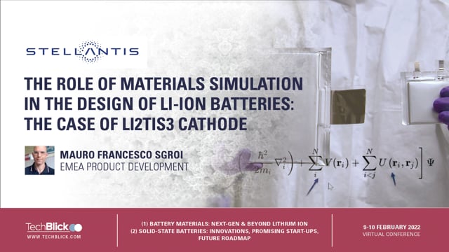
- The role of materials simulation in the design of Li-ion batteries: the case of Li2TiS3 cathode
Speaker: Mauro Francesco Sgroi | Company: Stellantis | Date: 9-10 Feb 2022 | Full Presentation The current worldwide effort to electrify the private transport sector is based on the availability of Li-ion cells with high specific energy, long cycle life and acceptable cost. Electrodes and electrolytes materials play a fundamental role in determining the performances of Li-ion cells. The use of critical raw materials, such as cobalt and graphite, is a crucial aspect for the LIBs market and novel materials have to be developed. Computational materials science is widely used to design new materials and to optimize the properties of the existing ones: in the field of Li-ion cells this approach led to a deeper understanding of many chemical-physical phenomena associated with the operation of the cell. After a general introduction, the main computational approaches to simulate the Li-ion cells materials will be presented including DFT methods and molecular dynamics. Finally the talk will concentrate on the development of a robust and predictive DFT method for the description of a disordered cubic Li2TiS3 system, a cobalt-free high capacity material showing promising properties as cathode in all-solid-state Li batteries. Join TechBlick on an annual pass to join all live online conference or online version of onsite conference access library of on-demand talks (600 talks + PDFs) portfolio of expert led masterclass year-round platform https://www.techblick.com/ Our next battery-related event will take place on 15-16 FEB 2023, covering 1) Solid-State Batteries: Innovations, Promising Start-Ups, & Future Roadmap 2) Battery Materials: Next-Generation & Beyond Lithium Ion The speakers include: General Motors, Graphenix Development, Brookhaven National Laboratory, Fraunhofer IKTS, RWTH Aachen University, Lawrence Livermore National Laboratories, Meta Materials Inc, Skeleton Technologies, Solid State Battery Inc, Argonne National Laboratories, OneD Battery Sciences, VTT, Leyden Jar Technologies B.V., b-Science, Rho Motion, Wevo-Chemie, LiNA Energy, CNM Technologies, Ionblox, Empa, Zinc8 Energy Solutions, Avicenne Energy, Echiontech, South8 Technologies, Basquevolt, NanoXplore, Chasm, Li Metal, Sila Nanotechnologies, Quantumscape (tentative), Fraunhofer ISI, etc https://www.techblick.com/
- High-Resolution Printing from 2D to 3D for Additive Manufacturing of Printed Electronics
Speaker: Doyoung Byun | Company: ENJET Inc| Date: 11-12 May 2021 | Full Presentation Bio Doyoung Byun received the PhD degree in Mechanical and Aerospace Engineering from the Korea Advanced Institute of Science and Technology (KAIST), Korea, in 2000. He has worked in several institutes and academies and founded the Enjet in 2009 in order to commercialize his high resolution printing and coating technologies for the printed electronics. Since 2009, he has served as CEO in the Enjet. He has developed the novel femto-liter droplet dispensing technology, electrostatic spray nozzle for functional coating, micro-fluidic devices, and MEMS devices. Based on these core technologies, he could commercialize ultra-fine printing and spray coating solutions for OLED display, micro-LED display, mobile phone, and bio-medical applications. The Enjet is a high resolution inkjet printing solution leader and has a vision to provide innovative tools of printed electronics (2D and 3D), replacing conventional vacuum processes in OLED, PCB, Semiconductor, Glass, Bio-medical, and energy industries. The Enjet has further dreams to develop 3D additive manufacturing solutions for printed electronics. The Enjet has been developing a high resolution inkjet head with multi-nozzles, which can dispense higher viscous ink than the conventional ones and form pico-liter or even femto-liter droplets. With this novel inkjet head, we can print and manufacture 3D electronic devices from the provided model data and personal customized products. Join TechBlick on an annual pass to join all live online conference or online version of onsite conference access library of on-demand talks (600 talks + PDFs) portfolio of expert led masterclass year-round platform https://www.techblick.com/ And do NOT miss our flagship event in Berlin on 17-18 OCT 2023 focused on Reshaping the Future of Electronics. This event attracts 550-600 participants from all the world and offers a superb ambience and dynamic exhibition floor. To learn more visit https://www.techblick.com/electronicsreshaped To see feedback about previous event see https://www.techblick.com/events-agenda
- World’s First hBN-Based Deep Ultraviolet LED
A Korean research team has developed a deep-ultraviolet (DUV) LED with an entirely new material. The DUV LED refers to a semiconductor light source designed to emit ultraviolet (UV) light with a short wavelength of 200 to 280 nanometers. Irradiating this LED on viruses or bacteria destroys harmful pathogens while minimizing harm to the human body. A POSTECH research team led by Professor Jonghwan Kim and Ph.D. candidates Su-Beom Song and Sangho Yoon (Department of Materials Science and Engineering) has produced DUV LED for the first time using hexagonal boron nitride (hBN). The team’s work was published in the journal Nature Communications. Unlike visible light, UV light can destroy or alter the form of a material. Among UV lights, the near-UV light has high penetration depth and can cause diseases when the skin is exposed to it. However, DUV light has extremely low skin penetrability and is anticipated to be safely used. For this reason, research to develop DUV LEDs has been active, mainly using aluminum gallium nitride (AlxGa1-xN). However, this material has a fundamental limitation in that its electroluminescence rapidly deteriorates as the wavelength becomes shorter and fabricating LEDs that can be used in the DUV frequencies remains a challenge. Hexagonal boron nitride (hBN) used by Professor Jonghwan Kim’s research team is a van der Waals (vdW) layered material like graphite. It is often called the ‘white graphene’ because its monolayer structure is similar to graphene and is transparent. Unlike AlxGa1-xN, it emits luminescence at DUV frequencies and therefore considered an effective new material for developing DUV LEDs. However, it has been difficult to inject electrons and holes due to its large bandgap*1, rendering it difficult to make into an LED. To this, the researchers focused on injecting electrons and holes to the hBN band edges by applying a strong voltage to the hBN nanofilm inducing the tunneling mechanism. With this, the researchers successfully fabricated an LED device based on a van der Waals heterostructure stacked with graphene, hBN, and graphene. Subsequent DUV micro-spectroscopy confirmed that the newly fabricated device emits strong UV light. “The development of a new high-efficiency LED material in a new frequency can be the starting point for pioneering groundbreaking optical device applications that have never been seen before,” remarked Professor Jonghwan Kim who led the study. “It is significant that this study presented the first demonstration of a deep-ultraviolet LED based on hBN.” He added, “Compared to the conventional AlxGa1-xN material, the new material has significantly higher efficiency of luminescence and enables miniaturization. It is anticipated to be highly applicable in viral and bacterial sterilization systems, semiconductor device manufacturing processes, and short-range wireless communication in the future.” Recently published in the world-renown journal Nature Communications, this research was conducted with the support from the Senior Researcher Program of the National Research Foundation of Korea and the Institute for Basic Science. *1. Bandgap The minimum energy required for electrons bound to a semiconductor or insulator to escape. More information: https://www.postech.ac.kr/eng/worlds-first-hbn-based-deep-ultraviolet-led/?pageds=2&k=&c=
- Electronic Skin That Can Feel in Real-Time
POSTECH-UNIST joint research team proposes a dynamic sensory system using artificial receptors that generate spike signals. The newly developed system enables real-time response that mimics real skin and achieves structural simplicity. We can pick up objects and take steady steps thanks to the tactility in our hands and feet. As such, skin acts as a channel that connects the external world or stimuli with the human body. When these sensory functions do not work properly, it becomes difficult to grasp or use objects, or in worse cases, fail to protect ourselves from dangerous external stimuli such as heat that can cause burns. Therefore, it is paramount for electric skin – being developed for artificial skin or humanoid robots – to be capable of reacting to the external environment in real time. A POSTECH research team led by Professor Unyong Jeong and Ph.D. candidate Taeyeong Kim (Department of Materials Science and Engineering) in collaboration with Professor Sung-Phil Kim and Ph.D. candidate Jaehun Kim (Department of Biomedical Engineering) at UNIST has developed an electronic skin that can sense tactility just as humans do. Conventional electronic skins could only process tactile information by sequential measurement of electric signals coming from the vast number of pixels configured in the sensor. Thus, densely packed pixels took much time to measure, rendering it difficult to create an electronic skin with a high spatial resolution that responds immediately to stimuli. The skin’s sensory receptors1 generate a spike signal2 spectrum in the form of electric potential in response to an external stimulus and recognize it by analyzing the signal pattern in the brain. The researchers took a hint from this signal generation and recognition mechanism of the skin’s sensory system to develop an artificial sensory receptor that generates spike signals on its own and created an electronic skin that can send all signals simultaneously to be analyzed in real-time. Since a biosignal lacks information on location, it is difficult to recognize a dynamic external stimulus in the high spatial definition. To overcome this limitation, the researchers presented for the first time that the artificial spike signals can be characterized to contain the position information. Equipped with this functionality, the e-skin can analyze spatial information such as position and motion trace, and temporal information such as speed and dynamic contact area. Since all artificial receptors in an e-skin transmit signals with only one pair of measuring electrodes, the electrode structure has been simplified compared to the conventional e-skins. Applying this technology to an actual robot, the researchers confirmed that the artificial skin reacts to external stimuli as humans do. “Our body steadily generates electric signals thanks to the flexible nature of electrolytes,” explained Professor Unyong Jeong of POSTECH who is a co-corresponding author of the study. “Understanding the biosensory mechanisms and developing methods to actualize them with electrolyte materials, we anticipate the e-skin to be applicable to recover tactility in damaged skin in patients and make robots with the ability to emotionally connect with humans. Professor Sung-Phil Kim of UNIST, the other co-corresponding author of the study, remarked, “Converting the external stimuli into spike signals and processing them is a groundbreaking idea that mimics how the human nervous system processes information.” He added, “If a new AI model is developed using this spike information encoding method, robot tactile intelligence can be further developed and effectively applied to next-generation semiconductor technologies such as neuromorphic chips.” Published in the international journal Science Robotics, this study was conducted with support from the Basic Research Laboratory Program and the Brain Convergence Research Program through the National Research Foundation of Korea. 1. Receptors sensory nerve endings that respond to various stimuli 2. Spike signal An electrical signal that generates a voltage and then disappears due to a change in the distribution of ions in the receptor when there is an external stimulus. More information: https://www.postech.ac.kr/eng/electronic-skin-that-can-feel-in-real-time/?pageds=1&k=&c=
- Smart LED Contact Lenses for Treating Diabetic Retinopathy
Diabetes is a long-term chronic disease with many complications and requires care over a lifetime. The longer a patient suffers from diabetes, the higher the risk of developing retinopathy which can progressively lead to a decline in vision and even to blindness. A POSTECH research team led by Professor Sei Kwang Hahn and Ph.D. candidate Geon-Hui Lee (Department of Materials Science and Engineering) in collaboration with Dr. Sangbaie Shin of PHI BIOMED Co. has recently developed a smart contact lens-type wearable device to prevent diabetic retinopathy and treat it in its early stages by irradiating 120 µW far-red/LED light to the retina. This technology for smart LED contact lens has attracted great attention for various ophthalmologic diseases. Diabetic retinopathy is currently treated by highly invasive repeated therapeutic injections to the eyeball or thousands of small burns made with a laser to destroy capillaries near the edges of the retina under anesthesia. Both procedures are considered highly painful for the patient. Through the study with diabetic animal models, the researchers confirmed that the diabetic retinopathy did not appear in animals that wore the smart contact lenses for 15 minutes 3 times a week for a total of 8 weeks. In contrast, the animals that did not wear the lenses showed retinopathic conditions. The safety and effectiveness of the lenses were also confirmed by the histological analysis of the cornea and retina. "This study has demonstrated the feasibility of a lens-type wearable device for the applications not only to monitoring oxygen saturation, heart beating rate, and ophthalmologic diseases but also to treating depression, insomnia, neuronal diseases and more," remarked Professor Sei Kwang Han who led the study. Published in the international academic journal Advanced Science, this study was conducted by the support from the Nano · Material Technology Development Program, Disease Oriented Translational Research, Mid-career Researcher Program, Brain Korea 21 Fostering Outstanding Universities (FOUR) project, and the Korea Medical Device Development Fund of the National Research Foundation of Korea, and by the World Class 300 Project of the Ministry of SMEs and Startups of Korea. For more information: https://www.postech.ac.kr/eng/smart-led-contact-lenses-for-treating-diabetic-retinopathy/?pageds=1&k=&c=