
On-Site Masterclasses
Eindhoven 2022
The Future of Electronics RESHAPED
There will be two parallel tracks of industry-led masterclasses on 11 October 2022, the day before the conference. Each 45-min masterclass will cover a technology or application in detail, offering an insightful blend of practical, technological and application knowledge. These masterclasses will be delivered by industry experts & may involve live demonstrations.
The content below describes the outline of the classes. Please note that you will be able to move between tracks at the end of each class. The numbers in each class are limited, and will be allocated on a first come, first served basis. PDFs of all masterclass presentations will be made available online to masterclass attendees.
Due to overwhelming demand these masterclasses are now sold out. On-demand recordings of these masterclasses however will be available on the TechBlick virtual platform for TechBlick members.
Masterclasses | Track 1
9:00 AM
Advanced Functional Screen Printing: Advances and Techniques for Ultra Fineline Printing Copy

John Lau
Asada Mesh
In this class, you will learn about all aspects of advanced functional screen printing. You will learn about insightful practical advice on all aspects of screen printing. In particular, the instructors will focus on practical as well as application knowledge and advice on how to print ultrafine features reliability, approaching sub-25um linewidths. This will consider the impact of mesh, substrate, ink, and other influential parameters.
10:00 AM
Industrial Inkjet Printing

Kai Keller
Notion Systems
You will learn about all aspects of functional inkjet printing technology. You will learn about different inkjet printing approaches as well as the pros and cons of each option. You will learn about the latest techniques to further the resolution of digital inkjet printing for single and multi-head techniques, e.g., electrohydrodynamic printing. Finally, you will learn about the development of industrial level inkjet printing of complex functional materials.
11:00 AM
Flexible Hybrid Electronics Manufacture – An Overview

Dr Simon Johnson
CPI
This short tutorial will present an overview of the techniques and technologies used in the manufacture of flexible hybrid electronic (FHE) circuits. The fundamentals of the technologies will be discussed along with the assembly techniques and we will also consider the types of circuits that can be built with FHE. The benefits of the circuit form will be considered along with the challenges and some solutions.
12:00 PM
Introduction to LIFT (Laser Induced Forward Transfer): Technology and Challenges

Sergio Roso
Holst Centre
LIFT is an emerging digital printing technology, which some characterize as digitization of screen printing. This technique can achieve high-throughput digital printing of multi-materials on various substrates. Uniquely unlike inkjet printing, it can also handle highly viscous pastes and materials, thus uniquely opening a digital technique for their precision printing.
In this Masterclass, you will learn about the basics of the LIFT process, its current capabilities and limitations in terms of printable materials, viscosities, resolutions and printing speeds, and also recent technological advances enabling high-throughput integration of microcomponents (e.g., microLEDs) through printing of very fine interconnects and mass transfer assembly.
Masterclasses | Track 2
9:00 AM
Copper Inks Usage, Formulations and Applications

Ofer Shochet
Copprint
There has been a long-term desire and development to replace the well-established silver paste and ink technology. The copper technology is finally reaching a maturity point where long-standing issues are resolved, and the technology is gaining market acceptance. In this class, you will learn about various copper inks on the market, and the pros and cons of each approach, including conductivity, reliability, and curing techniques. You will learn about practical techniques and tips for applying and adopting copper inks, even in existing lines. You will learn important insights about scale up of copper ink production. Finally, you will learn about a large array of applications in which copper inks deliver value together with supporting data. These applications range from wafer-based PV to RFID to aluminium based LED boards and beyond
10:00 AM
Introduction to Solution-Processed Light-Emitting Materials: Quantum Dots, OLEDs

Dr. Manuel Gensler & Dr Yohan Kim
Fraunhofer Institute for Applied Polymer Research
In this class you will learn about printable and solution processible light-emitting materials, in particular focusing on quantum dots (QDs) and OLEDs. You will learn about these materials, their properties and their applications. Finally, you will learn about the technologies and challenges for printing these materials using inkjet and EHD-Jet on different substrates.
11:00 AM
Wearable Sensors for Healthcare Applications
Charlotte Kjellander
Holst Centre
With rising prevalence of chronic diseases, healthcare organizations are dealing with resourcing issues, enormous pressure on personnel, long patient waiting lists, and missed health screening appointments, further pressurized by the consequences of the recent coronavirus pandemic.
This more than ever highlights a need in a sustainable healthcare from economic, social, and environmental perspective.
Wearable skin sensors or ‘the smart skin’ offer new ways for remote monitoring to support the accessibility to and sustainability of healthcare systems along the entire care cycle: from healthy lifestyle to screening, diagnosis and post treatment surveillance.
Recent advances in technology printed electronics, in miniaturization of sensors and in photonics, have significantly contributed to the wearable technology. All of these sensors can be integrated into stretchable, flexible and breathable wearables which can be worn during weeks.
In this Masterclass you will learn about the Vital Signs wearable patch – an open platform for measurements of biophysical read-outs as well as about its potential applications for remote monitoring for well-being and heath. What is more, we will share how next generation wearable technology platform can address healthcare needs. We will also address challenges on the road ahead concerning manufacturing, durability of wear and signal reliability
12:00 PM
The Art of Roll-2-Roll Printing

Christoph Kaiser
Innovation Lab
InnovationLab’s Masterclass on “The Art of Roll-2-Roll Printing” gives insights into the topic of screen and flexo printing. It explains how feasibility meets producibility and shows the advantages of the printing techniques implemented at InnovationLab. Because function is more than looking nice, it investigates the new demand that emerged when it comes to the printing of electronics, including inks, tools and machinery. pen up with printed sensors.
Masterclasses | Track 3


Company Tours
These three tours are open to attendees on the morning masterclasses. There is no charge but places are limited. When booking your masterclass please email l Chris@TechBlick.com to confirm you wish to attend a tour.
The tours will commence at 1.30pm and attendees should meet at the registration desk where tickets will be handed out.

Tour1 Part B Metafas
Metafas: PE Production + demos
Printed Electronics Netherlands Association Tour
Tour1 Part B
Metafas
Metafas BV is the most advanced production facility for user intefaces and Printed Electronics in The Netherlands. It covers a DTP studio, printing production and assembly facility. It uses modern computers to screen (CTS) for preparation of the screens. Metafas works according to Dutch TÜV certified quality system ISO 9001-2015. Smart thinking in electronic printing! You will visit the production facility and see several examples of Printed Electronics Applications from The Netherlands. Metafas is located in Asten (appx 25 mins from HTCE) .

Tour1 Part A Suss MicroTec
SUSS MicroTec Netherlands B.V.

Printed Electronics Netherlands Association Tour
Tour 1 / Part A
SUSS MicroTec Netherlands B.V.
SUSS MicroTec Netherlands is a leading edge supplier of Inkjet printers for R&D and volume production. It provides state-of-the-art solutions for your individual requirements, which enables you to stay competitive in terms of technology and productivity. Inkjet printing is an additive manufacturing technology applying functional materials for a variety of applications. These functional materials can have dielectric, conductive, adhesive, mechanical, optical, or chemical properties, and are printed with pico-liter sized droplets from a digital file. Its precise drop placement and accurate drop volumes make functional inkjet printing suited to printed electronics, displays, OLED, sensors, PCBs, semiconductor assembly, chemical machining, photovoltaics, life science and optics. Visit our lab facility and get insights into our state of the art printers and applications.
See: www.suss.com/en

TNO at Holst Centre & Solliance
Printed Electronics labs (2D/3D) Printing, Thin-film solar research, Thin Film Electronics

TNO at Holst Centre & Solliance
We will take you on a tour of the facilities at the TNO at Holst Centre and Solliance, which is a short walk away from the conference centre. There are 3 different sections to this tour and attendees will be able to attend all 3. Numbers will be limited to 36 people, again on a first come, first served basis.
This tour+networking drinks will end at 5.45pm.
A) Printed Electronics labs (2D/3D) Printing
The Holst Centre lab on printed electronics encompasses S2S and R2R tooling for printed electronics prototyping and small series manufacturing. The lab has various screen printers and pick and place machines. Next to this, we also have finishing labs where for example we can integrate printed electronics with textiles or convert 2D printed electronics in 2.5D shapes through thermo-forming. Finally, we have a newly founded lab for 3D printed electronics.
B) Thin-film solar research (Solliance)
Thin-film solar research. Thin-film solar cells offer large possibilities in design and application since it is flexible, lightweight, and transparent. This next generation solar cells open the possibility to apply solar cells on any imaginable (curved) surface. TNO, partner in Solliance, is focussing its research on cell technology, optimising cell architecture, materials and production technology of perovskite based tandem solar cells. Deposition technologies are solution based printing technology and vacuum deposition technologies.
C) Thin Film Electronics
Thin Film Electronics process capabilities entail panel-level thin film technology on substrate sizes up to 32 x 35 cm2. Deposition technologies that are employed are e.g. sputtering, (PE)CVD and spin- and slotdie coating. In addition specifically developed large-area atomic layer deposition technology called Spatial Atomic Layer Deposition can yield very conformal thin films over large areas. Patterning of material layers is performed via photolithography and subsequent wet- and dry etching. The infrastructure is employed to realize integrated functional devices, such as thin film batteries, water electrolysis stacks and integrated microfluidic devices for Organ-on-Chip applications
Networking Drinks At The Experience Centre at Holst Centre
All attendees on the TNO at Holst Centre and Solliance tours are invited to some networking drinks at The Experience Centre. The Holst Centre is continuously pushing the boundaries of electronics with new form factors. The resulting innovations are leading a paradigm shift in application domains ranging from energy storage to healthcare. Our updated Experience Centre neatly captures some of these innovative applications. We cordially invite you for an informal get together at our Experience Centre, to see the showcased innovations up close, and to engage in interesting conversations with our experts. This is also a great networking opportunity, with drinks being served in a cozy setting

Tour1 Part A Fashion Tech
FashionTech: Texile Integration of PE

Printed Electronics Netherlands Association Tour
Tour 1 / Part A
FashionTech: Texile Integration of PE
The FashionTech Farm is a studio, incubator and production facility for integration of electronics in textile applications. The Farm was initiated by Dutch Designer Marina Toeters and now houses several fashiontech desiners and startups, including by-wire.net,LABELEDBY., Lithe Lab, Bilihome , Malou Beemer.
Visit this unique fashiontech facility and get guided around by the designers themselves.
FashionTech Farm is located near The Evoluon in Eindhoven (10 mins from HTCE)
See: www.fashionTechFarm.com

Tour1 Part A Domicro
Domicro: New PE Process Development

Printed Electronics Netherlands Association Tour
Tour 1 / Part A
Domicro
DoMicro BV is a technology company developing innovative manufacturing technology, application solutions and micro assembly technology for flexible hybrid electronics (FHE) and micro devices. DoMicro excels in developing cutting edge inkjet printing processes, micro assembly and 3D packaging technology. During the tour, you will be visiting the lab facility, clean rooms and get insights in the PE processes developed during the last decade.
Domicro is located near the Eindhoven Airport (appx 15 mins from HTCE)
See: www.domicro.nl

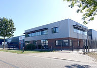
Morphotonics (Eindhoven 2022)
Revolutionary displays.

Morphotonics
This tour is limited to 15 people, and places will be allocated on a first come, first serve basis. Morphotonics is a 10 minute drive from the High Tech Campus, transport will be provided.
Morphotonics enables new revolutionary displays providing micro- or nano optics. With our Roll-to-Plate imprint technology optical components are made for cutting-edge products like Augmented Reality, anti-glare surfaces or 3D displays. The relative simplicity, scalability, and cost-effectiveness of this large area nanoimprinting method are attractive to a wide range of customers.
There will be a brief tour of their facilities including the R2P (Roll-to-Plate) machines operating in the clean rooms, only visible through windows. There will also be a 20-30 minute presentation about the company and technology (prior to facility tour).