


BrightSpot Automation | Customized defect imaging solutions for Perovskite and Tandem cell/panel architectures
- Aug 20, 2025
- 5 min read
Updated: Sep 17, 2025
#PerovskiteSolarCells #TandemSolar #Photovoltaics #SolarInnovation #DefectImaging #Electroluminescence #Photoluminescence #UVFluorescence #PVManufacturing #QualityControl #SolarTech #RenewableEnergy
Author: Andrew Gabor, BrightSpot Automation LLC, gabor@brightspotautomation.com
Perovskite PV technology faces severe challenges in scaling to the GW deployment level in terms of panel stability, conversion efficiency, and manufacturing yields. To help solve these challenges, BrightSpot Automation serves the entire Perovskite PV value chain with a suite of metrology tools implemented from R&D to product development to manufacturing to field testing. Our systems help identify defects, improve quality, reduce investment risk, and extend the performance of PV technology throughout its lifecycle.

BrightSpot supplies customized Photoluminescence (PL) and Electroluminescence (EL) imaging tools which assess device spatial uniformity and resolve defects such as pinholes between the Perovskite film and carrier transport layers. Such pinholes may cause shunts that reduce fill factor and increase sensitivity to reverse bias damage. BrightSpot also supplies UV Fluorescence (UVF) tools which reveal the effects of moisture ingress due to incomplete sealing. The table above shows which of these tools are applicable at different stages during manufacturing, accelerated testing, and field exposure.

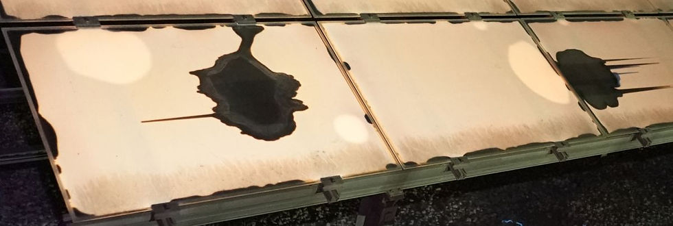
EL involves injecting current into the device with a power supply such that the device glows like a large LED in the near infrared (NIR), and then imaging the emission with an NIR sensitive camera. Any dark areas represent problems, and the overall strength of the emission is correlated to device quality. Prior to the metallization step, current cannot be injected electrically, but a non-contact PL image can still be captured instead by shining short-wavelength light on the partially processed devices and injecting carriers optically. The PL images are similar to EL images, but generally do not include the effects of series resistance problems (e.g. – contact resistance, metallization and TCO problems, wire problems). The cropped PL image here displays defects < 0.5mm in size even though the field of view of the camera was above 1m, showing the potential of the technique even for large-area manufacturing.

Detecting the bandgap of the Perovskite films is especially important to do immediately after deposition, and this can be accomplished by measuring the PL emission spectrum with a spectrometer over a small spot. The shape and intensity of PL (and EL) spectra can reveal more detailed defect information, though with a more limited spatial resolution than imaging techniques.

UVF involves stimulating fluorescence in encapsulant layers, revealing the presence of moisture and oxygen ingress following long field exposure or environmental chamber exposure. 2-terminal devices with Perovskite films deposited on silicon wafer cells incorporate encapsulant layers between the cells and the glass frontsheet and between the cells and the glass backsheet. Superstrate configuration devices that do not use silicon cells typically will only have an encapsulant layer in front of the glass backsheet. Frequently, encapsulant layers incorporate UV absorbing fluorophores to protect the panels from UV degradation, and with exposure to heat and/or UV radiation over the equivalent of months, the encapsulant layer will fluoresce when later illuminated by UV light. However, the UVF signal can be quenched by oxygen activity, and this feature enables the use of UVF to detect the location of sealing problems by the edges or junction boxes as can be seen here in the UVF images from the rear side a glass/glass silicon panel and the front side of a CIGS thin film panel (dark spots). In addition, the CIGS panel shows an interesting diffusion of oxygen down the length of the scribe lines, and this mechanism could be relevant to monolithically integrated Perovskite panels as well. The UVF technique is particularly valuable to implement during product development after any environmental chamber testing, and strongly fluorescing encapsulants could be used to strengthen the signal for such tests.

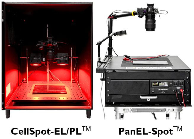
BrightSpot supplies both standardized and customized EL, PL, and UVF solutions for different size scales and for different applications. For R&D applications the CellSpotTM tool incorporates a lightproof enclosure and can be used for both cells and minimodules, whether on silicon wafers or glass. For applications that don’t fit within the enclosure, customized R&D EL/PL solutions can be built for tabletop use, and the PanEL-SpotTM tool can be used for any size EL application. For manufacturing, in-line systems can be supplied for silicon tandem cell applications and for minimodules and modules of any size. For outdoor testing, standardized EL (TravEL-SpotTM) and UVF (UVF-SpotTM) tripod or pole-mounted camera systems in Pelican travel cases can be supplied.

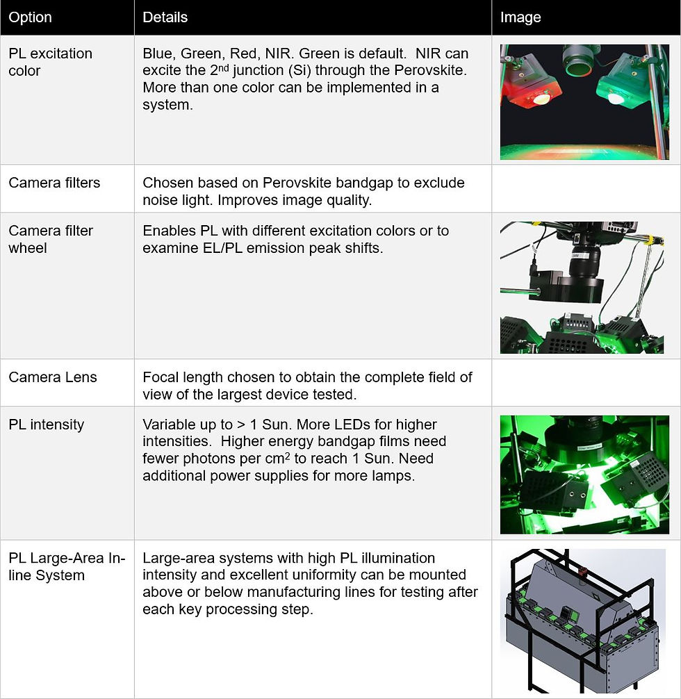
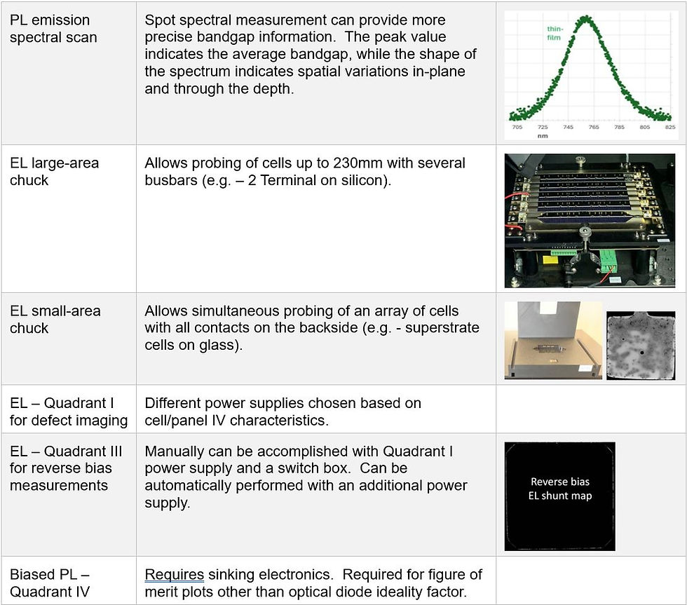
The table below describes the various customization options available for the EL and PL systems.
Software is a key part of BrightSpot systems. BrightSpot’s IMPELTM software talks to all system components – cameras, lenses, filter wheels, power supplies, relays, valves, motors, sensors, PLC’s, barcode readers, and other computers – whether in R&D enclosures, outdoor EL test kits, or integrated production line systems. Autofocus routines can ensure perfect focus every time. Captured images can be automatically enhanced through manipulations such as lens distortion corrections, perspective distortion corrections, contrast/brightness enhancement, autocropping of areas around the cells/panels, image colorization across several palette choices, and background noise (sunlight) removal. These enhancements can be applied as images are captured or later through manual post-processing, as well as individually or in a batch mode to an entire dataset. When required, multi-camera images of large panels can be automatically stitched together into a single composite image. All critical device control and image enhancement parameters are saved in Recipes for easy recall.

While the EL/PL images are valuable in their own right, quantification of the images is preferred for implementation in statistical process control of factory lines and in Design of Experiments. IMPEL includes many recipes which use linear/high bit-depth image formats to spatially resolve figures of merit related to familiar photovoltaic performance parameters. For example, a series of PL images at different calibrated intensities produces a map of the cell’s optical diode ideality factor as is shown here, revealing the specific characteristics of active recombination mechanisms across the film. A series of electrically-biased PL images can be captured to produce additional figure of merit plots such as series resistance, implied open-circuit voltage, and power conversion efficiency. Custom multi-step recipes can also be defined, for example to automate a series of images over time to examine various degradation mechanisms as stressors are applied. For closer manual inspection, the average and standard deviation of pixel intensity can be computed within a user defined region. Finally, defect types and grading can be defined to allow BrightSpot to create a customized AI inference model to automatically detect various defects and grade the resulting images.
We are Exhibiting in Berlin.
Visit our booth at the TechBlick Perovskite Connect event co-located with the Future of Electronics RESHAPED on 22-23 October 2025 in Berlin.
Contact us for your special discount coupon to attend
What I enjoyed most about using Zenhotels is the transparency. I was planning a trip to Moscow and wanted to be sure I wasn’t missing out on better deals, but after checking different sites, I realized Zenhotels فنادق في موسكو really offered competitive prices. The descriptions of each hotel were very detailed, and the real guest reviews helped me choose with more confidence. My hotel turned out to be exactly as shown on the site, which is not always the case with other platforms. For me, Zenhotels has become a go-to when looking for reliable bookings abroad.