


17 September 2024
Introducing the Program: Focus On Additive and 3D Electronics
TechBlick The Future of Electronics RESHAPED - Why You Should Join Us. 23 & 24 October 2024 | Berlin, Germany TechBlick have prepared a world-class agenda for you, featuring over 70 superb invited talks, 12 industry- or expert-led masterclasses, 4 tours, and over 80 onsite exhibitors. You can explore the full program here. In this article series, we highlight various talks in the program, outlining the technologies and applications that will be showcased. In this article, we discuss the theme of Additive and 3D Electronics, highlighting talks, masterclasses and tours from the likes of Airbus, Semikron Danfoss, Ceradrop, NeoTech AMT GmbH, Hasselt University, Karlsruhe Institute of Technology, Hahn-Schickard Institute, PERC, Binghamton University, University of Texas El Paso, Tecnalia. Note that this is the second article on the theme of Additive and 3D Electronics. In the previous article, we highlighted contributions from the European Space Agency, Yole Group, Decathlon, LPKF Laser & Electronics, Exxelia Micropen, Fuji Corp, Elephant, Nano OPS, Notion Systems, and Henkel and Tecna-Print, Printed Electronics Ltd, ImageXpert, Quantica. Explore and Register Before 11 October When The FINAL Early Bird Rate Ends Airbus will share their findings on the durability of 3D printed and hybrid electronics under aeronautic conditions. The motivation here is the direct integration of electronics on composite structures. In this case, flexible hybrid electronics embedded in TPU foils are i...

28 August 2024
Henkel Adhesive Technologies | Fine Line Silver Ink Printing: Essential Success Factors
Author: Thibaut Soulestin, PhD; Senior Application Engineer, Henkel Adhesive Technologies - Printed Electronics; thibaut.soulestin@henkel.com Henkel Adhesive Technologies holds leading market positions worldwide in the industrial and consumer business. As a global leader in the adhesives, sealants, and functional coatings markets, Henkel has developed a large material portfolio of LOCTITE® conductive inks and coatings suitable for printing electronic circuitry, that is thin, lightweight and flexible. The LOCTITE® Printed Electronics portfolio offers more than 100 different material solutions of which more than 20 are silver inks. Driven by the megatrend of digitalization, printed electronics offer a complementary solution to traditional electronic circuitry, opening new opportunities for electronics integration and miniaturization across industries. To achieve surface integrability, with limited visibility to the human eye, the printing of fine line structures has become increasingly important. To achieve high-performing fine line printed circuitry, it requires conductive inks having fine silver particles and adapted viscosity e.g. LOCTITE® ECI 1006. We are exhibiting! Visit our booth at the flagship TechBlick event in Berlin on 23-24 October 2024. Let's RESHAPE the Future of Electronics together, making it Additive, Sustainable, Flexible, Hybrid, Wearable, Structural, and 3D. 1. LOCTITE® ECI 1006 Among the large range of Henkel silver inks, LOCTITE® ECI 1006 is specific...

26 August 2024
Introducing the Program: Volume Manufacturing with Printed Electronics
TechBlick The Future of Electronics RESHAPED - Why You Should Join Us We have prepared a world-class agenda for you, featuring over 70 superb invited talks from around the world, 12 industry- or expert-led masterclasses, 4 tours, and over 80 onsite exhibitors. In this article series, we highlight various talks in the program, outlining the technologies and applications that will be showcased. In this article, we discuss the theme of volume manufacturing with printed electronics highlighting talks, masterclasses and tours from the likes of Flexoo, Avery Dennison Smartrac, SPGPrints, db-Matik, Beckermus Technologies, Printed Electronics Limited, Voltera, Tracxon, ImageXpert, Fraunhofer IZM, Quantica, Inuru, ScreenTec, etc In a previous article, we have already highlighted some of the talks focused on wearable, bio, and/or medical sensors as well as on digital and 3D additive electronics. In future articles, we will highlight more contributions on this theme as well as other key themes such as sustainable electronics, materials innovations, additive and 3D electronics, wearables and electronic textiles, medical electronics, photovoltaics, packaging, novel materials, lighting applications, etc. Stay tuned! Flexoo will outline their ability to offer mass customization as well as mass production with a specific focus on smart sensors and labels. Flexoo - a spin-off from InnovationLab GmbH with the direct acquisition of Heidelberg Printed Electronics GmbH - has created unique capabi...

20 August 2024
TechBlick | Introducing the Program - Smart Surfaces and Sensors
Why You Should Join TechBlick's The Future of Electronics RESHAPED? We have prepared a world-class agenda for you, featuring over 70 superb invited talks from around the world, 12 industry- or expert-led masterclasses, 4 tours, and over 80 onsite exhibitors. In this article series, we highlight various talks in the program, outlining the technologies and applications that will be showcased in the program. In this article, we discuss the theme of Smart Surfaces and Sensors including the automotive and human-machine interface sections. highlighting talks, masterclasses, and tours from the likes of Forvia, Momentive and BSC Computer, Motherson Innovations, Global Access Diagnostics (GADx), Datwyler, Würth Elektronik Group, Metafas, Holst Centre, and Arkema and KEMET. In a previous article, we already highlighted talks focused on wearable, bio, and/or medical sensors. In future articles, we will highlight more contributions on this theme as well as other key themes such as sustainable electronics, materials innovations, additive and 3D electronics, wearables and electronic textiles, medical electronics, photovoltaics, packaging, novel materials, lighting applications, etc. Stay tuned! Forvia - a global automotive supplier - will join us to give an invited keynote talk, outlining their strategy for automotive interiors using printed electronics including smart surfaces. The presentation will cover the specific use cases under development, and will zoom in on specific applicatio...

11 September 2024
Creative Materials Inc., Unveils Economical Conductive Ink and High Dielectric Strength Ink for Advanced Electronic Applications
Ayer, MA September 2024 - Creative Materials Inc., an innovator of materials for the electronics industry, is pleased to announce the launch of two new high performance ink products: 125-10ADP Economical Conductive Ink and 130-05GL High Dielectric Strength Ink. These advanced inks represent a significant advancement in the realm of electronic manufacturing providing enhanced performance, reduced costs, and greater reliability. 125-10ADP Economical Conductive Ink The 125-10ADP Economical Conductive Ink is designed to meet the growing demand for cost-effective solutions without compromising performance. This ink is user friendly, offers high mechanical strength, electrical conductivity and excellent adhesion to a variety surfaces, making it ideal for use in a variety of applications including membrane switches, flexible electronics, printed circuit boards (PCBs), and sensors. Key features of the 125-10ADP ink include: Reliability: Delivers consistent electrical performance with low resistivity. Cost-Effectiveness: Provides a high-quality solution at a competitive price, enabling cost savings for manufacturers. Versatility: Suitable for use on a wide range of substrates, including treated and untreated polyester, urethanes and polyimide. 130-05GL High Dielectric Strength Ink In parallel, the 130-05GL High Dielectric Strength Ink addresses the critical need for materials with outstanding insulation properties. This novel ink is engineered to provide high dielectric strength (2,50...

26 August 2024
Panacol-Elosol GmbH | Adhesive Solutions for Perovskite-based and Organic Photovoltaic Applications
Author: Dr. Lena Reinke | lena.reinke@panacol.de Perovskite-based (PSC) and organic photovoltaic (OPV) cells represent a promising frontier in renewable energy generation technologies due to their potential for lightweight, flexible and potentially cost-effective solar power generation. However one of the critical challenges in the commercialization and long-term reliability of OPV cells is their encapsulation. Effective encapsulation protects the delicate photoactive materials from environmental factors such as moisture, oxygen and mechanical stress. Adhesives play a crucial role in this encapsulation process, offering not only mechanical stability but also environmental protection. This article focuses on the various types of adhesives used in the encapsulation of OPV or PSC cells. We are exhibiting! Visit our booth at the flagship TechBlick event in Berlin on 23-24 October 2024. Let's RESHAPE the Future of Electronics together, making it Additive, Sustainable, Flexible, Hybrid, Wearable, Structural, and 3D. Encapsulation adhesives for OPV or PSC cells must meet several stringent criteria: Moisture and Oxygen Barrier: As the active materials are sensitive towards humidity and/or oxygen, the adhesive should therefore provide good barrier properties to prevent a degradation caused by moisture or oxygen ingress. The adhesive barrier properties can be tuned using to different strategies. One can either use quite hydrophobic raw materials to chemically prevent the ingress of w...

20 August 2024
Cu pastes for photovoltaics, invested perovskite solar cells, R2R OPV manufacturing, and inkjet printed perovskite PVs
In this newsletter, you can learn about the following technologies. We will have the opportunity to download the full slides. ISC Konstanz - Screen-printed Cu-pastes for highly efficient back-contact silicon solar cells Oxford Suzhou - Efficient and Stable Inverted Perovskite Solar Cell with modified Al as a Cathode OE Technologies - Roll2Roll High-Volume Manufacturing of OPVs Perovskia Solar AG - Perovskite solar cells for low-light applications The Future of Electronics RESHAPED Europe is the flagship TechBlick event. This event will take place at the Estrel Hotel and Convention Center (ECC) in Berlin on 23-24 October 2024. Explore the preliminary agenda here. 1. Screen-printed Cu-pastes for highly efficient back-contact silicon solar cells ISC Konstanz | March 2022 Screen printed Cu-pastes for high efficient back-contact silicon solar cells? In this slide deck you can learn about: ✅Accelerated growth of photovoltaics ✅Market growth of PVs and impact on silver consumption ✅Benefits of Copper vs Silver ✅Requirements for Cu based metallization ✅Properties of copper ink from Copprint ✅Back contact solar cells: ISC’s ZEBRA cell ✅Replacement of Bus Bars in ZEBRA ✅Line resistance Cu busbars ✅Results cell IV characteristic ✅Peel force results: soldering and ECA ✅Climate chamber tests ✅Thermal cycling results ✅Damp heat results ✅Conclusion and Outlook Download Presentation Slides 2. Efficient and Stable Inverted Perovskite Solar Cell with modified Al as a Cathode Oxford Suzhou |...
19 August 2024
Hamamatsu Photonics | Optimize printed electronics manufacturing with laser sintering
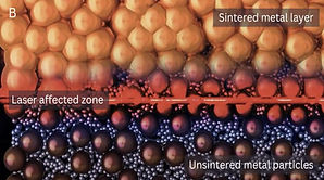
Author: Mr Naveen Balla, info@hamamatsu.de The production of printed electronics represents a transformative approach to manufacturing electronic devices. Switching from complex technologies like etching or lithography to a printing process significantly simplifies production, offering a cost-effective, versatile, and straightforward pathway to fabricating electronic components on various substrates. As a result, printed electronics are used in a wide range of devices, including flexible displays, thin-film transistors, sensors, and photovoltaic cells. While already common in various industries, production equipment for printed electronics still has room for improvement to optimize manufacturing efficiency. One important aspect of this optimization, especially when using metal nanoparticle inks, is the sintering process. The sintering step includes fusing the metal nanoparticles in ink ensuring the required low resistivity of the finished circuits. For this task, heating ovens, NIR emitters, and broadband flash lamps are established technologies, but they suffer from drawbacks that limit the speed or efficiency of production. In this article, we present five aspects of printing equipment that can be improved by switching to laser sintering. Table 1: Comparison of different sintering methods We are exhibiting! Visit our booth at the flagship TechBlick event in Berlin on 23-24 October 2024. Let's RESHAPE the Future of Electronics together, making it Additive, Sustainable, Flex...