


6 June 2022
DoMicro | Integration Of Thinned Bare Dies Using Inkjet Printing For Interconnections
The technology for integrating dies is one of the key enablers for the realization of new applications in flexible hybrid electronics (FHE), e.g. in in-mold electronics or smart glass. Using inkjet printing technology, DoMicro has developed a state-of-the-art approach for micro assembly. This approach enables the realization of demonstrators of advanced applications with for example ICs, passive components, sensors and LEDs. An example, described in this paper, is the demonstrator for wireless IoT devices with touch sensors and a Bluetooth chip. With the integration of ultra-thin bare dies, the total height of the demonstrator is below 0.7 mm. This thin form-factor enables smooth integration of functionality in various surfaces, labels, fabric etc. The inkjet printing technology brings several important capabilities, such as seamless and invisible integration, integration of thinned bare dies on flexible substrates and a reduced number of process steps. Configurations for die bonding and contacting A first step for the realization of the wireless IoT demonstrator was the investigation of the optimal configuration for die contacting and bonding. Several configurations have been studied. Figure 1 is showing a Fan In Ball Grid Array (BGA) configuration by inkjet printing on bare die. An inkjet-printed dielectric is covering the die while keeping the areas at the contact pads open. Next on top silver ink is connecting the bond pads to a BGA pattern on top of the dielectric coatin...

1 June 2022
Dupont Teijin Films | Polyester film solutions from DTF meeting changing needs in flexible electroni
This is an auto-transcriped version of the presentaiton without human control Thank you. Yeah. I've looked forward here, too, to give you a blitz update on the developments we have done to films for flexible electronic. Applications. And we are a company which is a global company which has six manufacturing sites across the world as an R&D centre where I personally work in the UK northeast of of, of England. We've been a long time in developing films for the applications of flexible electronics with since the early nineties with test strips, batteries, membrane switches, flexible circuits, diffuser vector films. And you may wonder why actually, apart from being a choice for sustainability point of view these days, why we actually use it now briefly, it's because of our process really, or about by actual rotation process. With the process at the end, it gives us superior properties for chemical, electrical, mechanical and optical and but not to go too much of that. What I want to show you is the scale of the production. Here we are making from half a market to 500 mark on thick films with run rates from 20 to 3 millimetres a minute and on a line of nine meters wide, that gives you 21 2000 square meters a minute. That's a large scale, but this is all just offered at low cost but has repercussions for minimum order quantities, of course. Now many applications in the flexible electronics are rely on DTF dimensionally stabilized rates and become more and more common with developme...

31 May 2022
Additive Electronics Update: MicroLEDs, Impulse Printing, Sub-Micron Printing, Solderable Copper Ink
This newsletter will provide regular updates in additive electronics covering the full and broad spectrum of materials, processes, and applicaitons. The term additive electronics encompasses an exteremely diverse set of technologies and applications. We will cover all. To learn more visit TechBlick online or onsite (www.TechBlick.com). Wrap-around electrodes for microLEDs To scale up microLED displays to large areas, smaller displays can be titled. Because microLEDs can be truely edge-less devices, the tiling can function, yielding a seemless look. Each title should house the microLEDs, backplane, as well as driver electrodes. The microLEDs and the backplane sit on the front side of the glass substrate whilst the driver electrodes are tucked away at the back. Interconnects are needed to connect the two. Wrap-around electrodes (interconnects wraping around the edge to connect front and back) is an elegent solution which bypasses the need for a drilled and filled through-glass via. The wrap around electrodes can be printed or PVD deposited (both prefer chamfered glass) . The latter can yield better feature sizes and thin and conductive lines, whilst the former can increase productivity. The below images demonstrate various technologies. Screen printing is a robust solution with low TACT time. Applied Materials has demonstrated that it can screen print very narrow (30um) linewidths over narrow spacings (50um). These are excellent results. Note, by way of reference, that state-of...

30 May 2022
Asada Mesh | Screen Printed Fine Grids for Transparent Capacitive Switches
Contact: Fernando Zicarelli, North America Business Manager – Asada Mesh Co., Ltd. Email: fernando@asada-mesh.page website: edu.asada-mesh.com Applications like HMI for automotive, home appliances, medical and aeronautical markets are driving the development of flexible transparent, capacitive switches. These switches enable a high level of differentiation and design freedom to make thin, ergonomic, and functional surfaces with attractive backlit schemes. To produce, functional layers of a Transparent Capacitive Switch (TCS) circuit are printed on a production scale screen printing line at e2ip technologies. Sun Chemical’s silver paste allows us to screen print <30 micron resolution of transparent metal mesh electrodes. The inks are printed on commercially available PET substrates (Ikonics) with Sun Chemical SunTronic inks (silver conductive ink, UV dielectric ink, carbon ink and other supplementary inks as needed for the target design) and using high-quality stainless screen mesh by Asada Mesh and screens prepared by Sefar Inc (with the latest emulsion technology from Kiwo). Fine Mesh Wire Technology (9-15 microns) allows for Thinner Depositions (2-5 microns). Visit our virtual booth High-Resolution Emulsion Technology allows for better edge definition and ultra-fine resolution (10-30 microns below). Visit our virtual booth PET Substrate technology has improved to help in the areas of Adhesion, Temperature Dissipation, preventing Paste Spread and obtaining Smaller...
6 June 2022
Scalable 3D Printed Electronics - from “Fully Additive” to High Volume
Speaker: Martin Hedges | Company: Neotech AMT GmbH| Date: 10-11 March 2021 | Full Presentation This presentation will review the state-of-the-art related to the production of 3D mechatronic systems using Additive Manufacturing (AM) and review developments for scaling the processes through all stages, from one off prototyping to high volume manufacture. A reconfigurable array of structural and electronics printing, pre- and post processing techniques are combined with SMD technologies to enable digitally driven 3D electronics manufacturing. The resultant flexible process chains can be easily reconfigured to cope with rapid changes in product type whilst retaining the ability to be scaled through to high volume manufacture. Selection of the most appropriate print, pre- and post-processing methods with the subsequent effect on process speed and cost will be discussed. A brief review of current applications, spanning 3D electronic circuits, antenna, sensor and heater patterns will be conducted along with an update on the progression to First Time Right manufacture of complex devices. Join TechBlick on an annual pass to join all live online conference or online version of onsite conference access library of on-demand talks (600 talks + PDFs) portfolio of expert led masterclass year-round platform https://www.techblick.com/ And do NOT miss our flagship event in Berlin on 17-18 OCT 2023 focused on Reshaping the Future of Electronics. This event attracts 550-600 participants from a...
31 May 2022
Additive Electronics Update:Rolling Nanolith, Intense Light Soldering,
Printing in Si PV, Stretchable Substrates, Autonomous Printing, Low-T Inks This article reviews diverse technologies in the world of additive electronics including rolling nanolithography, intense light solder sintering/reflow, front side metallization trends and roadmap in Si PV, high-T SMT-compatible stretchable susbtrates, autonomous coating and printing, low-temperature silver NP inks, etc. Please do join our Innovations Festival on 24 June 2022 (online) when these and many more interesting technologies will be presented. You can also join us onsite in Eindhoven (12-13 Oct 2022) to meet the global community in-person. Learn more here Rolling Nanolithography: Industrial R2R process for creating micron and sub-micron feature sizes Rolling nanolithography can take the linewith resolution of R2R lighography even below 1um. This technology, by Meta Inc (Meta Materials Inc) includes a roller around which a mask is wraped and within which a UV light sits. The wrap-aroud mask itself it manufactured using electron beam lithography, giving it very fine features. Therefore, the mask can support, like nanoimprint technology, nano-meter scale features. However, the UV exposure itself may limit feature size to 500nm or 1um range. The current web size is 300mm although Meta is developing technology to scale this to 1200mm webwidths. Here, a step-and-repeat process can be used to create larger rolling masks (note: there might be some 100um wide discontinuities and thus may not be fully s...
31 May 2022
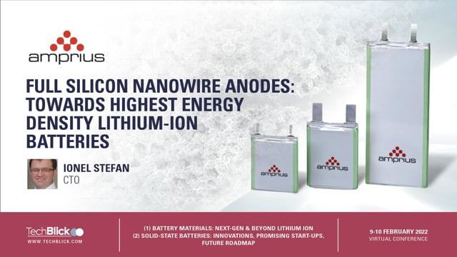
Full silicon nanowire anodes: towards highest energy density Lithium-ion batteries
Speaker: Ionel Stefan | Company: Amprius | Date: 9-10 Feb 2022 | Full Presentation The silicon nanowire anode technology addresses silicon swelling by enabling silicon to expand and contract internally, in a very robust mechanical structure. As a result, over 1200 Wh/L and 450 Wh/kg levels of energy density were achieved in lithium-ion cells with a cycle life in the hundreds of cycles and fast charging in under 10 minutes, enabling new devices and applications. Join TechBlick on an annual pass to join all live online conference or online version of onsite conference access library of on-demand talks (600 talks + PDFs) portfolio of expert led masterclass year-round platform https://www.techblick.com/ Our next battery-related event will take place on 15-16 FEB 2023, covering 1) Solid-State Batteries: Innovations, Promising Start-Ups, & Future Roadmap 2) Battery Materials: Next-Generation & Beyond Lithium Ion The speakers include: General Motors, Graphenix Development, Brookhaven National Laboratory, Fraunhofer IKTS, RWTH Aachen University, Lawrence Livermore National Laboratories, Meta Materials Inc, Skeleton Technologies, Solid State Battery Inc, Argonne National Laboratories, OneD Battery Sciences, VTT, Leyden Jar Technologies B.V., b-Science, Rho Motion, Wevo-Chemie, LiNA Energy, CNM Technologies, Ionblox, Empa, Zinc8 Energy Solutions, Avicenne Energy, Echiontech, South8 Technologies, Basquevolt, NanoXplore, Chasm, Li Metal, Sila Nanotechnologies,...

30 May 2022
Innovations Festival: Printed, Hybrid, 3D, InMold, Textile Electronics (50 free spots available)
24 June | 2.00pm - 7.00pm CET | Virtual Event Platform TechBlick has announced its online Innovations Festival (24 June 2022 | 14:00 to 19:00 CEST | 8:00 to 13:00 EST), showcasing a broad spectrum of innovative technologies from around the world in the field of Printed, Hybrid, Flexible, InMold, 3D, Structural, and Textile Electronics. This must-attend event showcases exciting and cutting-edge advances from across the world. It brings together more than 400+ participants, 45 speakers and 55+ live exhibitors. The audience is truly global, coming together across many different time zones.
See the full programme here and register here https://www.techblick.com/PE-festival-2022 There are 50 free spots thanks to our sponsors assigned on a first come first serve basis The LIVE virtual exhibitors in the special session will include: Coatema Machinery GmbH, Nagase, Eastman Kodak, Panasonic, Applied Materials, Nano-Ops, CPI, Elantas, Seristampa, Quad Industries, Brilliant Matter, Kimoto, Sateco AG, Fujikura Kasei, Metamaterials Inc, Fujifilm, ACI Materials, Fraunhofer IAP, Panacol, Keiron Printing Technologies, InnovationLab GmbH, Electroninks, Eastprint, Jet Metal, DuPont Teijin Films, Liquid Wire, Sunray Scientific, Asada Mesh, Copprint, Holst Center, Neotech AMT GmbH, XTPL, Brewer Science, Agfa, Belink Solutions, MacDermid, GiS, Voltera, DoMicro, DuPont, Raymor, Ynvisible, others. Full Agenda...