


How Femtosecond Lasers are Advancing the Consumer Electronics Field
- Sep 8, 2025
- 4 min read
Deividas Andriukaitis (Main Author) [1], Paulius Gečys[2], Tadas Kildušis[3]
[1] Ekspla, Vilnius, Lithuania | [2] Center for Physical Sciences and Technology, Vilnius, Lithuania | [3] Akoneer, Vilnius, Lithuania
Contact: d.andriukaitis@ekspla.com, Deividas Andriukaitis
The consumer electronics field continues to evolve rapidly, driven by tighter tolerances, higher quality, faster processing speeds, and novel functionalities. As manufacturing demands increase, femtosecond lasers have become an essential technology, playing a critical role in enabling these advancements. In this article, we explore how femtosecond lasers are shaping the development of consumer electronics and powering emerging manufacturing technologies.

Lasers have long contributed to technological progress across various domains - from telecommunications and metrology to automotive, semiconductor, and medical sectors. Among the different laser types, femtosecond lasers stand out due to their extremely short pulse duration (on the order of 10⁻¹⁵ seconds). When tightly focused, they enable highly localized energy delivery in both time and space, vaporizing material with minimal thermal effects - a process known as „cold“ ablation.

![To learn more about MicroLED and AR/VR displays please join the show in Eindhoven on 24 and 25 Sept 2025. Learn more [here]](https://static.wixstatic.com/media/953b95_ea7a0a157938469cb02b0f45b8bf242b~mv2.jpg/v1/fill/w_650,h_180,al_c,q_80,enc_avif,quality_auto/953b95_ea7a0a157938469cb02b0f45b8bf242b~mv2.jpg)
Thanks to this ultrashort energy deposition, femtosecond lasers can ablate materials before heat spreads into surrounding areas. Compared to nanosecond lasers, this results in superior processing quality, minimal heat-affected zones, and the ability to machine brittle or thermally sensitive materials such as polymers, ceramics, and metals. In many cases, the resulting quality is so high that no post-processing is needed, simplifying the overall production chain.

At Ekspla, we’ve been designing and manufacturing laser systems for over 30 years, with the mission of delivering reliable solutions for both scientific research and industrial applications. Our FemtoLux series of femtosecond lasers is widely used in micromachining tasks where precision and surface quality are essential.
Through regular collaboration with customers, we've gathered a wide range of successful use cases that demonstrate the advantages of femtosecond laser processing.
Glass, being transparent, brittle, and hard, is a natural fit for femtosecond laser processing. Applications include cutting, drilling, milling, scribing, dicing, and etching. One process gaining momentum is the creation of through-glass vias (TGVs) - narrow, deep holes in glass substrates used in advanced semiconductor packaging. A single glass interposer can contain thousands of these features, demanding a process that’s both reliable and scalable.
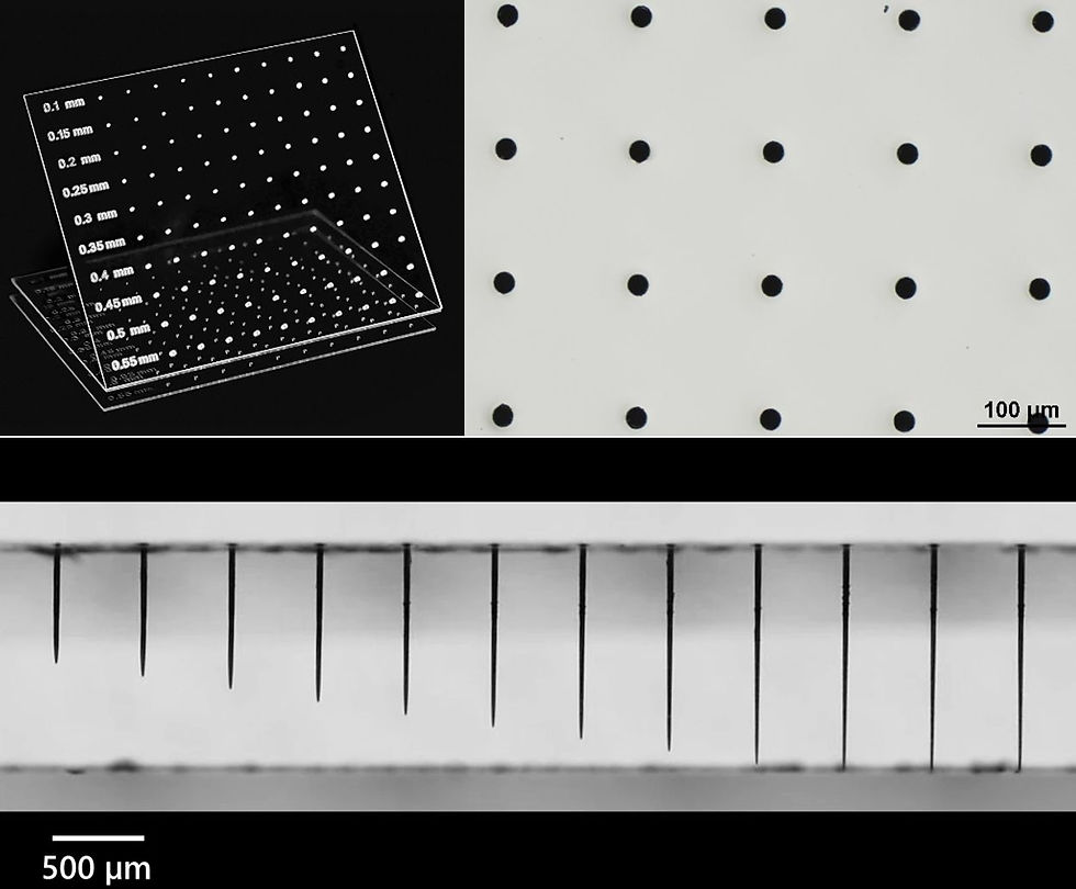
Our FemtoLux 30 has proven effective for both ablation-based and selective laser etching approaches to TGV production, across materials such as Eagle XG and Borofloat 33. Its broad parameter tunability makes it well-suited for handling the material variability seen in different glass types, making it a strong candidate for high-precision glass micromachining tasks.
Polymers pose a different challenge. Many are highly sensitive to heat, making it difficult to process them without damage. Femtosecond lasers, due to their minimal heat-affected zone, are ideal for this task. While most femtosecond lasers operate at 1030 nm, switching to shorter wavelengths can further reduce thermal effects. In one case, a customer working with a thermally sensitive polymer was dissatisfied with a 23 µm heat-affected zone at 1030 nm. By switching to the second harmonic (515 nm), absorption improved significantly, reducing the heat-affected zone to just 8 µm - well within the required tolerances.

Femtosecond lasers also excel in metal micromachining, offering burr-free edges and negligible heat-affected zones. This enables the production of intricate metal parts without the need for secondary operations. We’ve successfully demonstrated processing on stainless steel, aluminum, copper, brass, and nitinol, as well as multilayer foils used in battery and energy storage applications.

Beyond material removal, femtosecond lasers are unlocking new possibilities in additive manufacturing and electronics fabrication. One standout example is Selective Surface Activation Induced by Laser (SSAIL) - a laser-based metallization method to complement or replace traditional photolithography. While photolithography offers high resolution, it comes with significant cost and complexity. Meanwhile, additive methods like inkjet printing offer flexibility but are often limited in speed and scalability.
SSAIL addresses this gap by enabling the creation of copper traces with resolutions down to 1 µm and throughput comparable to lithography - while maintaining the simplicity and digital control of additive approaches. The process begins with laser modification, where an ultrashort pulse laser selectively alters the substrate’s surface, introducing microscale structural and chemical changes. These modified regions are then subjected to catalytic activation by immersion in a metal precursor solution, which binds selectively to the laser-processed areas. Finally, an electroless plating process deposits a uniform copper layer only on the activated regions, resulting in precise and conductive traces. With its combination of resolution, speed, and simplicity, SSAIL presents a strong case as a next-generation technology for electronics manufacturing.

Femtosecond lasers are already playing a crucial role in advancing the consumer electronics field by enabling high-precision, high-quality processing of a wide range of materials. As demand grows for tighter tolerances, smaller features, and more efficient production methods, the importance of ultrafast
laser technologies will only increase. With ongoing improvements in performance and integration, femtosecond lasers are set to become an even more central tool in developing next-generation electronic devices. At Ekspla, our FemtoLux line of femtosecond lasers is well-positioned to support this progress - offering the flexibility, reliability, and precision needed to meet the challenges of tomorrow’s manufacturing.

Comments