


HPCaP: A New Technology for MicroLED Manufacturing
- Aug 15, 2025
- 7 min read
Updated: Aug 29, 2025
Authors: Julien Vitiello, Elisa Duquet, Louis Caillard, Achille Guitton, Marc Pascual, Maroua Ben Haddada, Frederic Raynal, Amin M’barki
Corresponding author: julien.vitiello@hummink.com
Hummink S.A.S, 5 rue Charlot, 75003 Paris, France
Keywords: Display repair, additive manufacturing, High Precision Capillary Printing (HPCaP), capillary forces, Atomic Force Microscopy (AFM)
Abstract
In the field of display repair, particularly for OLED and microLED technologies, there is a growing need for precise and scalable solutions to restore high-resolution defects without compromising performance. While several repair methods exist, they often fall short in resolution, versatility, or ease of integration. High Precision Capillary Printing (HPCaP) overcomes these limitations by leveraging capillary forces and mechanical resonance to deposit inks with micron and sub-micron precision, enabling accurate, reliable, and non-destructive repair of critical display components.
1. Introduction
According to MarketsandMarkets the global display market size is expected to reach around USD 174 billion in 2029 growing at a CAGR of 5.1% from 2024 to 2029. The increased demand for displays in various industries especially the IT and healthcare industries, and the increased demand of interactive displays such as wearable devices, AR/VR products in addition to the adoption of flexible displays are the major factors driving this market growth.

MicroLED production processes for displays face significant challenges, as many screens are rendered defective. These defects often manifest as non-functioning black pixels or pixels displaying incorrect colors, typically caused by faulty LEDs or malfunctioning circuit boards. Despite meticulous manufacturing practices, such errors are nearly inevitable, resulting in rejected displays that hinder productivity, increasing cost and waste.
The defects in these displays are increasingly microscopic, often below 5 micrometers, making traditional repair methods insufficient. LED defects can also vary widely, from line breaks and particle contamination to pixel malfunctions, requiring versatile and precise repair solutions. HPCaP (High Precision Capillary Printing) by Hummink is currently the only technology capable of printing at micron and submicron scales and thus repairing micronic defects.

2. High Precision Capillary Printing (HPCaP)
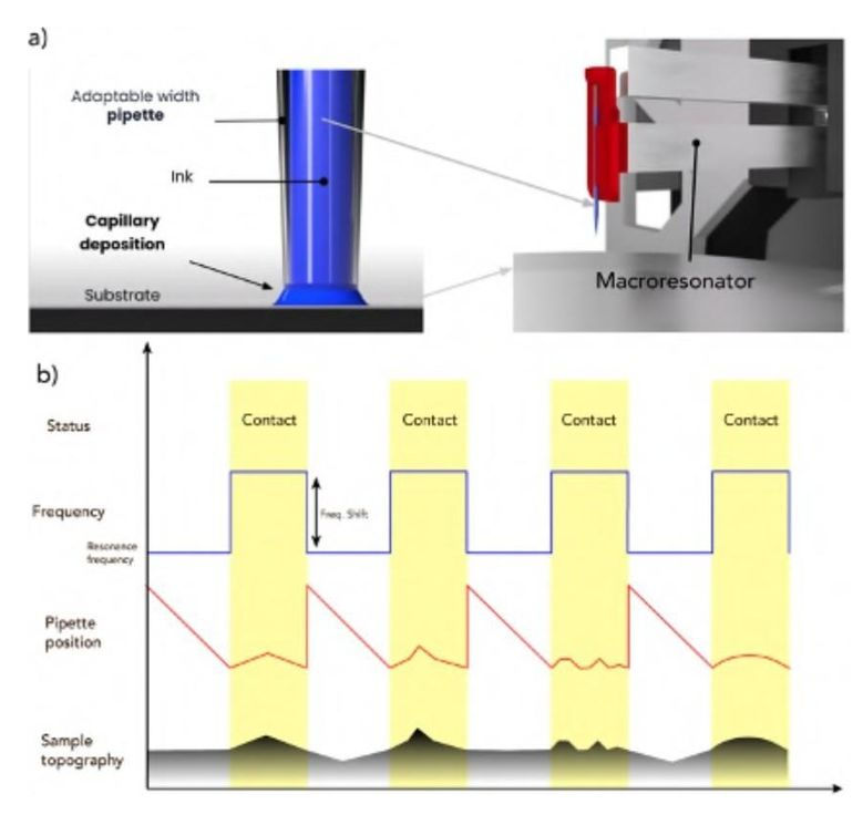
HPCaP is a technology strongly inspired by Atomic Force Microscopy (AFM) [1].It uses a macroscopic resonator as a detecting mechanism for contact and printing feedback. The uniqueness of this technology resides in its usage of capillary forces and resonance as the only driving force for printing.
A macroresonator oscillating at a resonance frequency of about 1 kHz is attached to a mechanical bridge. The oscillation is generated by a piezodither that excites the macroresonator. The bridge, driven by a piezostage, allows the resonator to move with a 5 nm precision in Z axis. State-of-the- art electronics are used to control the resonance of the macroresonator through 3 different parameters: the resonance phase, amplitude, and frequency. Any shift in these values can be controlled to achieve different printing features, indirectly modifying the print geometry (thickness, line width...). Amplitude can be adjusted between 5 nm and 100 nm, and any frequency shift of 100 mHz or more can be accurately detected. A pipette is attached to the extremity of the macroresonator and oscillates in phase with the latter.
Since the dispensed volume is in the nanoliter range (orders of magnitude lower than the pipette volume), a single pipette can print up to hundreds of kilometers, depending on the dispensing diameter.
Fig.1,(a) shows that the first step of the HPCaP printing process is to approach the pipette to the substrate surface. As the macroresonator is oscillating at its proper resonance frequency, a slight change of a few hundreds of mHz can be observed as in figure 1,
(b) once a meniscus is formed between the ink inside the pipette and the substrate. This meniscus is stabilized by the macroresonator’s oscillation, and the frequency shift is then locked by the electronic feedback loop. After this initial step, capillary printing can be achieved by moving the substrate in the XY axis. As the frequency shift value must remain constant, the Z-fine bridge will move the resonator in the Z direction to perfectly follow the topography of the substrate.
Fig. 2 presents the results of high-precision printing using a pipette with a 1.5 µm diameter. (a) displays a cross-section from a 3D map revealing a printed silver line with a thickness of 100 nm achieved in a single pass. (b) shows a 3D topographic map acquired with a Hitachi TM4000PlusII SEM. (c) is an SEM image of the printed pattern, consisting of three silver lines with a linewidth of 2.5 µm and a gap of 1.5 µm. These lines exhibit a bulk conductivity of 6 µΩ·cm. Thanks to the versatility of the ink formulation, HPCaP enables the printing of virtually any material. Fig.3 shows polymer (Polyvinylpyrrolidone) lines with a linewidth of 430±40 nm and a pitch of 1±0.05 µm. Similar sub-micronic gratings were printed with SU8 to create a distributed feedback laser [2].


3. Results
In this section, we showcase the key outcomes and repair capabilities of Hummink’s HPCaP technology in the context of display repair. The HPCaP printhead addresses a critical industry challenge: repairing high-resolution defects that conventional tools cannot handle, ultimately boosting production yield and salvaging previously discarded panels. In fig 4 we highlight a typical process that is used for display repair. As seen in this schematic, HPCaP technology can be used in tandem with laser etching to deposit conductive lines as well as encapsulating polymers. To achieve this, several capabilities must be demonstrated by HPCaP technology:
micrometric resolution and precision for defect correction.
Substrate versatility and automatic adaptation to substrate topography.
Diverse material compatibility.

3.1. Micrometric Resolution for Defect Correction
Achieving micron and even sub-micron resolution is essential for the repair of fine-line defects in MicroLED displays. As shown in figure 2 and 3, HPCaP enables material deposition at nanometric precision, allowing seamless restoration of damaged conductive paths or pixels without degrading the display’s visual or electrical performance. This ultra-fine control ensures that repaired traces maintain the original geometry and conductivity, which is crucial for optical consistency across the screen.
3.2. Substrate versatility and automatic adaptation to substrate topography
Substrates to be repaired are typically already patterned and can be a combination of different materials with topology variation. An advantage of HPCaP is that printing can be done on any substrate following its topography completely automatically.
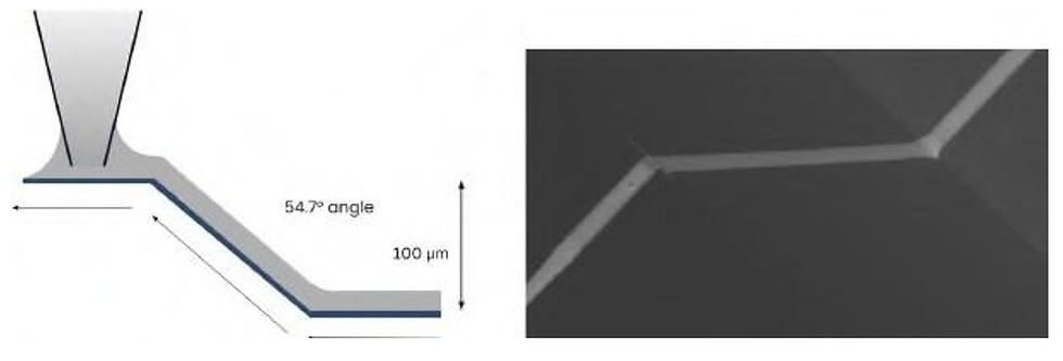
HPCaP has successfully printed on surfaces with topographies, fig.5 shows a silver trace of line width 10 µm printed on wet-etched silicon wafer with a step of 100 µm and a slope angle of 54.7°. To climb the step, the printing speed was decreased from 200 µm/s on flat wafers to 25 µm/s on the slope part. HPCaP functions like an AFM, enabling automatic printing on diverse topographies without the need for additional commands in the g-code. Advanced electronics in the printing process continuously gather feedback from the substrate, adjusting the pipette's z-axis movement to match its topography and facilitate precise printing accordingly.
3.3. Diverse material compatibility
Being able to print different inks on the same substrate is crucial for display repair. This versatility can be leveraged to be able to deposit conductive lines as well as encapsulating polymers with the same technology. The strength of capillary forces allows HPCaP to print inks with viscosity ranging between 0 to 100,000 cP. With minimal adjustments in rheological, capillary, and colloidal properties, any ink can be printed. In fig.6, we demonstrate the ability to print conductive silver lines of 2 µm linewidth and 2 µm pitch on a silicon wafer and coat these traces with a polymer (PVP). Such encapsulation is often required to prevent electrical shorts and oxidation of the metallic traces. The same ink can also be used to fill cavities and can be printed on with conductive ink after reticulation.

3.4. Display repair
HPCaP has successfully printed conductive lines on multimaterial patterned substrates to repair defective conductive lines. No damage has been observed on underlying TFT devices
4. Conclusion
As MicroLED technology advances, defects in displays are becoming smaller and more diverse, increasing the need for precise, scalable, and reliable repair solutions. HPCaP’s innovative printing technology offers a transformative approach to repairing LED displays, ensuring minimal waste and optimal production efficiency. Hummink is also currently working to expand this sustainable strategy to other industries, such as semiconductor packaging.
5. References
[1] Canale, L., Laborieux, A., Mogane, A. A., Jubin, L., Comtet, J., Lainé, A., Bocquet,L., Siria, A., & Niguès, A. (2018).Micromegascope.Nanotechnology, 29(35),355501. https://doi.org/ 10.1088/1361-6528/aacbad
[2] Pascual, M., Bigan, N., M’Barki, A., Mental, R.,Allegro, I., & Lemmer, U. (2023). All-printed SU8- perovskite DFB Laser. Advanced Fabrication Technologies for Micro/Nano Optics and Photonics XVI. https://doi.org/10.1117/12.2661336


Comments