Search Results
Search this site
1075 results found with an empty search
- Conformal EMI shielding based on particle-free inks
Conformal EMI shielding is a megatrend on its way to become ubiquitous in electronics. The incumbent process is based on sputtering a tri-layer structure consisting of SUS (stainless steel)- Cu-SUS (total stack is 3-6um typically) on the EMC (epoxy molding compound) of the package. Hikaru Uno from Merck & Melbs LeMieux from Electroninks Incorporated show an alternative based on non-vacuum spray coating of particle-free Ag inks. In these slides, you can see performance analysis and detailed cost analysis/projections. The incumbent (sputtering) is a well established technique with many market reference from the likes of Apple and Samsung. However, it is a vacuum process requiring substantial CapEx investments with a large production footprint. The sputtering deposition rate will also be low given the required film quality. Sputtering is poor at side wall and deep trench coverage, resulting in large thickness variations between the top and side walls. Spraying the EMI shielding can address some issues: it is a non vacuum process with a low Capex and a high unit-per-hour (UPH) throughput and is able to offer uniform side and top wall coverage. The spraying can be used with Ag or Cu nanoparticles. Both nanoparticle techniques though suffer from expensive materials, potential for nozzle clogging and thus production downtime, and even relatively thick required coatings. To overcome these shortcomings, particle-free silver inks can be sprayed. Is this technique effective? The below slides show shielding effective upto 40GHz with 1.2 and 3um coatings. This seems to meet the requirements. Is it reliable? In the slides below you can reliability data showing no measured change in sheet resistance of the package-level coated when subjected to a prolonged duration of harsh conditions Is it cost effective? Sputtering has a high capex cost as well as relatively high labour costs. However, spraying has higher ongoing material consumption costs.The slides below shows that spraying can be a very cost competitive approach Already commercial? It is still in sampling. The main stumbling back is the ever underestimate power of incumbency and already sunk CapEx investments in sputtering lines On the process, as shown below, the package is first pre-treated with plasma. The particle-free ink is then sprayed whilst the packages on the chuck are held at 160-200C. The elevated temperature results in rapid particle formation during the spray. Finally, after spraying, the inks are then cured for 20min@140-160C. There are relatively low curing temperature compared with other particle-free inks on the market. With the first successful market reference using spraying, the market gates will open, lifting all ink-based techniques and making this a part of fast-growing electronic packaging industry To learn more visit www.TechBlick.com TechBlick #printedelectronics #conductiveink #electronicpackaging #emishielding #sip #5g
- CNB Film Heaters for ADAS Sensors to Enable Any-Weather Safe Autonomous Driving
Speaker: Mari Makkonen | Company: Canatu| Date: 10-11 March 2021 | Full Presentation The presentation focuses on CNB film heaters for ADAS camera and LiDAR sensors, covering ADAS market evolution, constraints to ADAS uptake, side effects of fair weather on LiDAR and camera systems, challenges associated with the conventional heating wires and the limitations can be overcome to improve safety and reliability. During the presentation, optical test results and integration possibilities will also be shared. CNB heaters help vehicles “see” better and provide clear field of vision for ADAS systems to operate. These wire-free film heaters provide even heating and low optical distortion enabling accurate object detection. They can be 3D formed and either laminated or injection molded to provide a robust structure. Join our session to learn more! Mari Makkonen Marketing Director @ Canatu Oy Bio Marketing Director of Canatu, a carbon nanomaterial company, with extensive experience in global B2B technology marketing from nanomaterial, health tech, fire suppression and IT industries. Extensive experience in global B2B technology marketing from nanomaterial, health tech, fire suppression and IT industries. Join TechBlick on an annual pass to join all live online conference or online version of onsite conference access library of on-demand talks (600 talks + PDFs) portfolio of expert led masterclass year-round platform https://www.techblick.com/ And do NOT miss our flagship event in Berlin on 17-18 OCT 2023 focused on Reshaping the Future of Electronics. This event attracts 550-600 participants from all the world and offers a superb ambience and dynamic exhibition floor. To learn more visit https://www.techblick.com/electronicsreshaped To see feedback about previous event see https://www.techblick.com/events-agenda
- Innovation in a Pandemic
Speaker: Stan Farnsworth | Company: NovaCentrix| Date: 10-11 March 2021 | Full Presentation Even with the challenges of the past year, innovation has moved forward. Stan will take a look at how a few of the key tech trends have fared in the past year, such as 5G, AI, and IoT. He will also connect those to the printed and flexible electronics space, and why we should pay attention to those universal trends. Finally, he will touch on his own experiences with innovation at NovaCentrix, and consider aspects of sustaining innovation versus true disruption. Join TechBlick on an annual pass to join all live online conference or online version of onsite conference access library of on-demand talks (600 talks + PDFs) portfolio of expert led masterclass year-round platform https://www.techblick.com/ And do NOT miss our flagship event in Berlin on 17-18 OCT 2023 focused on Reshaping the Future of Electronics. This event attracts 550-600 participants from all the world and offers a superb ambience and dynamic exhibition floor. To learn more visit https://www.techblick.com/electronicsreshaped To see feedback about previous event see https://www.techblick.com/events-agenda
- Molecular inks: UV sintering and extreme formability for complex IME applications
Molecular particle free inks can offer extreme formability and stretchability, allowing the design and production of 3D shaped and/or in-mold electronics parts with extreme curvatures and complex shapes. Arnold Kell and Julie Ferrigno showcased some unique properties of these inks- together with IME possibility- at a TechBlick conference in May 2022. Some unique features are: 1- UV sintering: you can see in the slide below how the transparent clear molecular inks can be UV sintered (x5 times faster than thermal cure). At first, the clear inks absorb very little UV light. However, as Ag particles begin to precipitate out, the absorption grows. The higher absorption in turn raises the temperature, accelerating the sintering and resulting in higher UV absorption. This process continues until the ink is fully sintered and then self stops because then the particles reflect the light back like a mirror. 2- Partial sintering compatible with InMold Electronics: as part of the IME process, a thermoforming step is required. In this step, the substrate temperature is raised in a controlled fashion to soften the material, allowing it to be formed. In the proposed scheme, the printed molecular inks are first only partially cured by UV light. The full sintering then takes place in-situ by the elevated temperature of the 3D thermoforming process. This is an interesting approach because it enables faster curing and also allows one to sinter molecular inks on low-T substrates like PC. 3- Extreme formability: The 3rd slide belows shows comparison of these molecular inks with other standard inks. It shows that these inks can be stretched upto 50% with comparatively little change in resistance. This can be because these printed lines are very thin, and are thus able to follow the contours of the stretched substrate far better than a thicker particle-filled ink/paste 4- Unique shaped: The shapes enabled by IME are often limited by the formability of the inks. These inks can liberate the designer from such limitations, allowing the design and production of complex shapes with extreme curvatures. Here, an award-winning example is showcased by Julie, showing steep curves (see the controlled knob) Molecular inks are an exciting class of new inks. They have many application area. In fact, if formulated in higher viscosities, they may even support ultrafine screen printing since they avoid mesh clogging. To learn more about the world of printed electronics, join us in the Netherlands on 12-13 OCT 2022 https://www.techblick.com/electronicsreshaped #inmoldelectronics #printedelectronics #ime #3delectronics #molecularinks
- R2R grown GaN LEDs on metal foils instead of expensive sapphire wafers?
R2R grown GaN LEDs and perhaps even GaN/AlGaN HEMT transistors on metal foils instead of expensive small-area sapphire substrates? This could be a breakthrough technology, bringing the robust and efficient inorganic LED technology to large-areas. In microLED displays, it could mean monolithic integration, leading to mobile-sized and large displays manufactured without a wafer-to-substrate transfer step. As shown below, iBeam Materials is developing such technology. It first planarizes a rough metal foil and then uses an ion beam to form a nm-thick layer with aligned grains. This 'template' then acts as the growth substrate in lieu of, say, a sapphire wafer. As seen below, this technology has already been used to demonstrate a functional GaN LED as well as a GaN/AlGaN HEMT. In July 2021 (when the results were presented at TechBlick) the PL was upto 70% of normal LEDs. However, a direct comparison is not yet fair as the standard approach benefits from decades and decades of accumulated know-how and production expertise. Currently, the LEDs are still not done in a R2R fashion, although the 'template' can be R2R manufactured on 20"-wide substrate. The next step of development will involve demonstrating a R2R MOCVD GaN growth. The R2R production of the template is not the bottleneck, but the growth of a thick (5um or so) GaN LED Finally, Vladimir Matias argues that this technology has the potential to lower cost of production by a factor x25. A detailed cost analysis is shown below, demonstrating the technical milestones which need to be achieved to enable this cost roadmap. To learn more about this talk and about microLED join TechBlick first-ever specialist event on microLEDs: www.TechBlick.com/microLEDs #microLED #microLEDs #GaN #HEMT #Display #Lighting #R2R #MOCVD @klauz kunze
- "The Future of Electronics RESHAPED" Event Reports High Demand For Exhibition Booths & Attendees
TechBlick, the leading platform for emerging technologies, has reported high demand for both exhibition booths and attendee places at its inaugural in-person event which takes place on 12 & 13 October at the High Tech Campus in Eindhoven. The Future of Electronics RESHAPED conference and exhibition is the most important upcoming industry event in printed, hybrid, 3D, in-mold, textile & wearable electronics. As well as a world-class agenda and exhibition the event will also feature expert-led masterclasses and company tours to some of the innovative companies in the Eindhoven area. Khasha Ghaffarzadeh, CEO of TechBlick reported "We were surprised at the high demand for exhibition booths and fortunately we were able to secure some additional exhibiting space. But we still have a waiting list of companies wishing to exhibit. We have seen the same high demand for attendee places with companies excited by the quality of the speaker programme and exhibitors. This event will be where the world’s printed electronics industry connects and does business and is an important new event in the emerging technologies calendar" The world-class agenda features speakers such as Meta/Facebook, GE Healthcare, ASML, Airbus, Forvia, Schneider Electric, Stabilo, Forvia, Novo Nordisk, Identiv, JC Decaux, ABInBev and many more. See the full speaker list here. The vibrant exhibition floor features over 50 exhibitors including NanoDimension, DuPont, Eastman Kodak, FujiFilm, Henkel, Applied Materials, MacDermid Alpha, Holst Centre, Voltera, Panasonic and many more. See full list here Events are also about learning and experiences, which is why TechBlick have designed a fantastic day of expert-led masterclasses and tours on Tuesday 11 October (the day before the conference & exhibition). For further information click here. Attendee places are limited and demand is high so be sure to book your place soon - www.TechBlick.com
- Evolution of touch surfaces - integrating decorative film, capacitive touch, and haptic function in
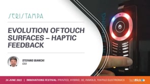
In the below presentation, Stefano Bianchi from SERISTAMPA SRL, shows a fully functional molded device made out of a combination of decorative film (in-mold decoration or IMD), printed capacitive touch film, and a haptic device. This injection molded device integrates push button, rotary knob, two linear slides, tactile feedback, etc It is an excellent and complex demonstrator, truely the advancing the art of in-mold electronics to integrate aesthetics, sensing, and tactile feedback Note that Seristampa is a leading industrial screen printing company specialized in advanced interactive service based in north of Italy. To reach this level of technological capability, Seristampa has evolved from aesthetical overlays/decorative parts to capacitive overlays/IML/IMD to capacitive films/printed electronics/IME and finally now to haptic device combining also all previous functionalities To learn more please visit Seristampa pages on TechBlick https://www.techblick.com/exhibitors Anne Rita Belke Gisella Tanzini #printedelectronics #haptics #tactilefeedback #IME #InMoldElectronics #3DElectronics
- High-res metalization of 2D and 3D object made from glass, ceramic, PET or thermosets?
The traditional LDS (laser direct structuring) process is fantastic but only works on special plastic substrates containing an sub-surface activation particles. This limits the choice and functionality of materials. Firstly, it typically does not work with glass, ceramics, PET or thermosets. Furthermore, the addition of activation particles can render a transparent material opaque or eliminate bio-compatibility. Furthermore, the linewidth resolution is typically around 80-100um (but can be pushed further down) with surface roughness of 20-30um Nouhad Bachnak , 3D-MID from Sunway Communication unveils a new process below, which promises to overcome these limitations. Here, the process first involves a special laser structuring process followed by a so-called chemical activation step. After this step, the structured and activated part undergoes typical plating (Cu-NiP-Au) The details of the chemical activation step - possibly the most important step- were not disclosed. Nonetheless, the disclosed examples and results indeed suggest that it can work on glass, ceramics, thermosets, etc. This is an important development and advancement of the technology, because it greatly lessens the limits on the choice of materials which can be 3D metallized with bulk-like properties and solderable surfaces Furthermore, it is argued that this process- presumably when optimized- will achieve 5um linewidths with a surface roughness of just 2-3um (great for antennas, for example). It can also plate within vias with 40um diameter. This is still not the full production level for all substrates. The most advanced development is for thermoset, which is production ready. The other substrates like glass, PET, and ceramics are still in development. Nonetheless, it is a good space to watch Hear more about this technology at TechBlick's inaugural onsite event on 12-13 OCT 2022 in the Netherlands https://www.techblick.com/electronicsreshaped
- Smart skin patches: a key enable of digital technology
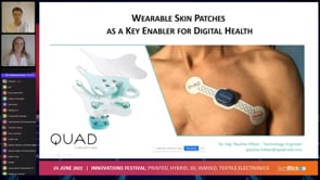
Smart skin patches are a rising trend, finding applications in sleep monitoring, EEG and brain activity monitoring, cardiovascular monitoring, and even in electrical stimulation of neurons, muscles, and other areas. These patches must meet many criteria- from signal quality to bio/skin compatibility to wearable to breathability to stretchability and to low cost production. Here, you will hear from Pauline Hibon on the requirements for skin patches as well as a general overview of some potential health-related applications To achieve low-cost volume production, screen printed electronics is essential. Quad Industries is well positioned in this area with its 1M/year patch production capacity. It can do R2R and S2S screen printing in Belgium and Slovakia, respectively. More importantly, it has already built extensive know-how and production expertise in the field with different designs and is thus an excellent prototyping and production partner. To learn more and visit the Quad Industry team, join the global industry in Eindhoven (the Netherlands) on 12-13 OCT 2022 https://www.techblick.com/electronicsreshaped Arne Casteleyn #printedelectronics#skinpatches#wearablesensors#medicalwearablesensors#eeg#BCI#insomnia#heartrate
- 3D-shaped mechanically-compliant soft force, pressure, or proximity sensors?
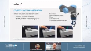
3D-shaped mechanically-compliant soft force, pressure, or proximity sensors with ease of integration and good reliability data? Daniel Haefliger from Sateco Group presents its non-printed technology based on multilayers of moulded conductive silicone. This is a unique technology. The sensor typically has a size of 10-40mm with a thickness of >3mm. It can measure forces in the range of 10-100 N with a resolution of around 0.1 N. The sensor can follow the direction of applied force for some 1mm. Interestingly, the exact behaviour of the sensor can be designed and adjusted by controlling the spaces between the layers to suit specific application requirements. The technology is reliable. It is shown that at room temperature, it experiences only 5% driff when subjected to 5,000,000 cycles of 20N force. It experiences only 20% drift over full scale when subjected to 100k cycles of 20N force at much harsher conditions (T range: -40 - 85C | RH: 0-90%) In clip from Daniel's full presentation given at TechBlick in March 2022, you learn about some unique applications of this technology, including: 1- Collaborative robots: these robots work alongside or in close proximity to humans. They are not caged as are typically industrial robots. As such, they require integrated soft 3D sensors to measure proximity as well as impact. This Sateco technology is uniquely suited to this application. 2- Smart steering wheel: the moulded silicone force sensor technology can be integrated within the centre of the steering wheel. They provide soft touch input and still enable the airbag to be deployed. 3- Wearable devices: in this example, developed with Fraunhofer Institute for Industrial Engineering IAO, they show how the sensor can be integrated into pagbacks to measure the load that children bear when carrying their bags Join us on 12-13 OCT 2022 to learn more about this super exciting technology and how it can enable 3D soft touch and force sensors https://www.techblick.com/electronicsreshaped Martina Mergl #silicone #keypads #cobots #HMI #3Delectronics #forcesensors #touchsensosrs #robots #wearabes #steeringwheel for applicaiton info watch this video for technical info on product and reliability check out
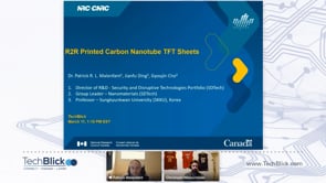
- Fully R2R printed TFTs with highly purified semiconducting SWCNTs?
Printed TFT has been a difficult technology to develop given the complex multi-layer nature of TFTs with their high sensitivity to interfacial and film quality properties. Here (from March 2021), Patrick R. L. Malenfant et al showcases R2R printed TFT sheets with good mobility and low VT variability even over a 10meter print run! Interestingly, SWCNTs have proven to be a good solution for the semiconductor layer of a printed TFT. SWCNTs are grown as a mixture of metallic (70%) and semiconducting (30%) tubes. Since there is no reliable method yet to only grow semiconducting types, one must separate the two. The best technique is based on use of conjugated polymers, which, through repeated rounds of centrifugation, enables one to disperse and thus separate CNTs based on diameter, chirality and type. This way one can obtain highly pure semiconducting-only SWCNT. Indeed, Raymor Industries Inc. is offering such materials already. The separated dispersions are not yet printable inks though. To formulate R2R printable inks, Patrick et al recommend a ligand exchange process to replace the hydrophobic polyfluorenes polymers (left over around the tubes as part of the separation process) with a more hydrophilic polymer. In the video below, Patrick shows that R2R printing of fully TFT is possible with excellent results: the TFTs have mobility range of 0.02-3 cm2/V.s, On/Off ratio of 1E4, and threshold voltage variability of around 6-10% over a 10m R2R print run! This technology shows the technological viability of R2R printed TFTs based on SC-SWCNT although there is still a long way to mature this technology into a production/commercial solution To learn more please join TechBlickwww.TechBlick.com #printedelectronics#TFTs#Carbonnanotubes#cnt#swcnt#R2R#displays#backplane#epaper National Research Council Canada / Conseil national de recherches Canada
- 3D formable diffuser substrates for integration of LED lighting with embedded printed electronics?
A prerequisite is often the right formable diffuser substrate! Here you can learn - from Menno Bos- about ultra formable PC-based light diffusion substrates, enabling one to combine LED lighting with embedded printed electronics over 3D surfaces with no heat spots! In the first example, a formable diffusion based on a clear 250um PC is shown, which can be stretched up to 200% (!!) with no edge thinning, enabling extremely complex 3D shapes. Decorative and functional inks can also be directly screen printed on its surface, enabling the integration of decorative patterns and electronic functionalities. This diffuser technology offers high light efficiency (80%) and good light transition (68%). It has many applications and here you will learn about applications in interior ambient lighting, overhead consoles, and exterior lighting. In the second example, Kimoto Europe introduces a new pre-cured stretchable hardcoat film co-extruded with a clear 250um-thick PC . This is a special pre-cured hardcoat surface which offers very high elongations (135/165%) whilst maintaining a good hardness (2-3H) To learn more join Kimoto in Eindhoven on 12-13 OCT 2022 https://www.techblick.com/electronicsreshaped TechBlick Christoph Bosshard #printedelectronics#automotiveinteriors#lighting#3Delectronics#LED#whitegoods#automotivelighting#touchsurfaces#InMoldElectronics#IME