Search Results
Search this site
1075 results found with an empty search
- Electrohydrodynamic Printing: Breaking the Limits of Inkjet
EHD is one of the most exicintg developments in the additive electronics field. It offers several key advantages over traditional inkjet: (1) it can achieve lower resolutions beyond current capabilities of inkjet, (2) can handle a wider range of ink viscosities, and (3) can cover non-flat topographies. EHD can print drops with <500nm diameters. It can reach 1-10um resolution, which standard inkjet would struggle to achieve. Furthermore, it can handle pastes with viscousities of some 1000 Cp. Given that the principle is based upon particles being pulled out by electrostatic force, whereas being pushed out by mechnical force as is the case with inkjet, the trajectory of the particles can be controlled, enabling one to print on 3D or non-flat topographies. These are all important technological steps forward. In the second slide, you can see examples of printing lines, droplets, and other patterns, demonstrated by Enjet. In the case of lines, one can see L/S ranging from 2/2um to 80/80um, demonstrating both the versality and also ultrafine line printing capabilities of this technology. In the inset, digital printing over a non-flat surface is shown, demonstraing good step coverage. A challenge for this technology is that it is slow. Most systems are R&D systems with a single head. However, companies are now developping industrial-scale mult-head printing. The embedded video shows a multi-bozzle array printing of 0.5-1um Ag NP lines by Scrona. This is a fantastic result because it shows a pathway towards industrial scale printing at ultra fine lines, beyond what inkjet achieves. Final slides show some applications. The application space is in fact broad and expanding. The EHD can be used to digital print micropads for placement of ever shrinking microLEDs (is the die attach a particle free Ag ink??); it can be used to print quantum dots (QDs) onto ever shrinking microLED dies, enabling color conversation; it can be used to repair printed metallizations and wrap-around edge electrodes for microLEDs or repair TFTs post production; it can be used in semiconductor packaging to digital print inteconnects or shielding; etc etc Join the TechBlick Innovation Festival (24 June- free | online) here to learn more. At this festival, Fraunhofer IAP will present the latest on EHD of QDs for display applications and DoMicro will present its perspectives on EHD printing, perhaps for die-first integration. 0.5- 1um Ag NP lines with multi-head EHD
- Digital printing with few micron resolution on non-flat surfaces with highly viscous pastes
Digital fineline printing is one of the most important developments in additive electronics. Inkjet itself has come very far with excellent progress even towards R2R industrialization. However, inkjet has two limitations as a technology: (1) limited resolution and (2) limited ink viscosity range. Here, we highly two technologies that can overcome these limits Here we highloght the microdispensing technology developed by XTPL with nozzle diameters in the range of 0.5-12um. It demonstrates a unique combination of ultrafine line (few micron) 'digital' printing on flat and non-flat surfaces AND highly conducting (4p% Ag bulk?) highly viscous nanoparticle (Ag, Cu, Au) pastes. Thus, this technology advances the art not just by extenting the resolution of digital printing beyond what inkjet achieves but also by enabling far more conductive and highly loaded conductive pastes. The innovation here is not just the microdispensing machine, but also the unique non-Newotonian highly-loaded nanoparticle pastes. The AgNP pastes have high loading (>85 wt% in some cases), small particles (45nm), and are in ethylene glycol solvents. The pastes require relatively high sintering temperatures (250-300C) but offer high conductivity, e.g., 4.2 uOhm.cm for the ink with 80wt% loading. In the first slide below you can learn about the microdispensing machine itself. It currently has a substrate size of around 50 mm x 50mm. The max print speed is around 10mm/s. Thhe XY motor and Z motor controllers have accuracies of 2um and 0.5um, respectively. In the next slide, what can see the types of structures that can be printed. In the benchmarking chart, it is demonstrated that they can achieve 2um linewidths with >40% bulk Ag conductivity, which outperforms other reports in the literature. In the right, one can see the types of structures being printed, showing that the printed structure demonstrate high aspect ratios. Given the highly loaded nature of the pastes as well as the narrow nozzle, fear of constant clogging exists. In the next slide, it is shown that the non-Newtonian pastes can be printed through a 2.5um nozzle for long periods of periods, demonstrating the stability of the process. In the final slide, we showcase the structures which can be printed.
- Why your next automotive heater will be a CNT hybrid
Speaker: Ken Klapproth | Company: CHASM Advanced Materials| Date: 10-11 March 2021 | Full Presentation Bio With more than 25 years of success matching technically advanced products to market demand, Mr. Klapproth has helped companies small and large achieve double-digit growth. He joined CHASM in 2019 bringing global expertise from leading sales and marketing organizations at companies including Desalitech, Elsevier, IHS, Entuity, Proficiency, and Siemens. Results-oriented and data-driven, Ken is fanatical about accelerating sales traction for technically complex products, cutting edge demand generation, is the holder of two U.S. patents, and believes electronics should be intuitive, integrated, organic, and – most importantly – NOT seen. Ken holds a BS in Mechanical Engineering from the University of Connecticut and began his professional career at Pratt & Whitney designing jet engines found under the wing on many of today’s modern aircraft including the Boeing 777. In his spare time, Ken is an avid woodworker, photography and video enthusiast, and runner. Join TechBlick on an annual pass to join all live online conference or online version of onsite conference access library of on-demand talks (600 talks + PDFs) portfolio of expert led masterclass year-round platform https://www.techblick.com/ And do NOT miss our flagship event in Berlin on 17-18 OCT 2023 focused on Reshaping the Future of Electronics. This event attracts 550-600 participants from all the world and offers a superb ambience and dynamic exhibition floor. To learn more visit https://www.techblick.com/electronicsreshaped To see feedback about previous event see https://www.techblick.com/events-agenda
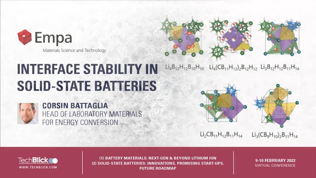
- Interface Stability in Solid-State Batteries
Speaker: Corsin Battaglia | Company: EMPA | Date: 9-10 Feb 2022 | Full Presentation Solid-state batteries combining an alkali metal anode and a high-voltage cathode have the potential to double the energy density of current-generation rechargeable batteries. We recently demonstrated the integration of hydroborate solid electrolytes with a 4 V class cathode through in-situ formation of a passivating interface layer. Combined with their high ionic conductivity > 1 mS/cm at room temperature, low gravimetric density 1.2 g/cm3, low toxicity, high thermal and chemical stability, stability vs lithium and sodium metal, soft mechanical properties enabling cold pressing, compatibility with solution infiltration, and potential for low cost, hydroborate electrolytes represent a promising option for a competitive next-generation solid-state battery technology. Join TechBlick on an annual pass to join all live online conference or online version of onsite conference access library of on-demand talks (600 talks + PDFs) portfolio of expert led masterclass year-round platform https://www.techblick.com/ Our next battery-related event will take place on 15-16 FEB 2023, covering 1) Solid-State Batteries: Innovations, Promising Start-Ups, & Future Roadmap 2) Battery Materials: Next-Generation & Beyond Lithium Ion The speakers include: General Motors, Graphenix Development, Brookhaven National Laboratory, Fraunhofer IKTS, RWTH Aachen University, Lawrence Livermore National Laboratories, Meta Materials Inc, Skeleton Technologies, Solid State Battery Inc, Argonne National Laboratories, OneD Battery Sciences, VTT, Leyden Jar Technologies B.V., b-Science, Rho Motion, Wevo-Chemie, LiNA Energy, CNM Technologies, Ionblox, Empa, Zinc8 Energy Solutions, Avicenne Energy, Echiontech, South8 Technologies, Basquevolt, NanoXplore, Chasm, Li Metal, Sila Nanotechnologies, Quantumscape (tentative), Fraunhofer ISI, etc https://www.techblick.com/
- SAFI-Tech | Supercooled Soldering™ Technology
Darin Heisterkamp, Head of Sales SAFI-Tech, Inc. darin@safi-tech.com Introduction Soldering technology is thousands of years old, but is still an essential component in electronics assembly, without which none of our advanced electronic devices would function. Though the soldering process has seen some refinement in modern times, it is still accomplished by heating the soldering metal alloy to its molten state and applying the metal hot at contact points to create a conductive solder joint. For today’s most popular tin-silver-copper (SAC305) soldering metal alloy, that processing temperature is in the range of 240 °C to 260 °C, and therein lies a huge problem. Design engineers developing the next generations of electronic products are being driven by consumer demand for new solutions that don’t conform to existing formats, are much smaller, and are more feature rich. Meeting this demand requires new materials that are thinner, lighter weight, and flexible, and designs that are more densely packed with increased miniaturization and integration. Unfortunately, such new products are completely incompatible with high-temperature soldering, but they still need the benefits of full metal conductive solder joints to function. New Supercooled Soldering™ Technology Figure1: Supercooled liquid metal microcapsule. Figure2: Calorimetry graph showing supercooled liquid range. SAFI-Tech has developed a new Supercooled Soldering™ technology using SAC305 that can solve this problem. Supercooling is a phenomenon that all materials experience at the phase transition from liquid to solid. SAFI-Tech’s micro-encapsulation process creates a new form factor that stabilizes the supercooled liquid phase of SAC305 inside a nanofilm shell, and extends the utility of this liquid phase to temperatures well below the alloy’s normal solidification point (see Figure 1). Now, SAC305 can be applied throughout this extended liquid range to form full metal conductive solder joints at temperatures best suited to each product design (see Figure 2). This novel solder interconnect technology avoids thermal damage to components and materials, as well as mitigates quality issues caused by coefficient of thermal expansion mismatch. SAFI-Tech supercooled liquid metal microcapsules appear as a fine powder, which can be incorporated into a typical solder paste formulation. Since the metal core inside the microcapsules is a liquid, it can flow out, wet, coalesce, and solidify to form a solder joint after action is taken on the shell. Similar to existing solder pastes, that action can be imparted by solder fluxes which dissolve the shell and release the liquid metal at a target temperature to bond opposing contact points (see Figure 3). Figure 3: Solder flux dissolves microcapsule shell to form solder joint. Product Demonstration SAFI-Tech demonstrates this supercooled soldering technology using SAC305 by attaching a BGA integrated circuit package to a printed circuit board at low temperatures. As BGA package dimensions increase with greater integration, integrated circuit components become more susceptible to thermally-induced dynamic warpage caused by the high temperature soldering process, which leads to attachment defects. For this demonstration, SAFI-Tech developed a prototype paste formulation and a flux with an activation temperature at 180 °C, over 60 °C below normal SAC305 reflow temperatures. This is also the same range where low temperature soldering with BiSn alloys occurs. The demonstration was set up as follows: Test Board - FR4 PCB - ImmAg Surface Finish - Electrical Testing Contacts Print Conditions - Steel Stencil with Steel Squeegee - 480 µm diameter aperture - 4 mil thickness Figures 4 and 5 show the print properties of the paste and the stenciled paste in the BGA grid pattern on the circuit board. Figure 4: Rheometry of prototype supercooled solder paste. Figure 5: Paste printed in BGA grid pattern Cross-sectional imagery of the BGA component after supercooled soldering shows good joint formation between the BGA SAC305 solder ball and SAFI-Tech’s supercooled SAC305 solder (see Figure 6). The BGA board assembly was sent to STI Electronics for preliminary analysis, where all BGA joints remained conductive with no failures after 1000 cycles of thermal shock (-40 °C to 110 °C). Figure 6: BGA with SAC305 ball attached to FR4 board soldered at 180 °C using SAFI-Tech supercooled SAC305 solder paste (Normal SAC305 reflow at 240 to 260 °C). Particularly interesting is the clear presence of the desirable Cu6Sn5 intermetallic compound (IMC) layer formed with SAC305 at this temperature (see Figure 7). Intermetallic compounds play an important role in the mechanical strength and reliability of the solder joint. Generally, an IMC layer less than 4 µm is preferred, and the supercooled soldering IMC layer was measured at 2.5 µm (see Figure 8). This is very similar to a typical IMC layer formed with SAC305 at conventional peak reflow temperatures. Figure 7: Cross-section of SAFI-Tech supercooled SAC305 solder joint interface showing intermetallic compound (IMC) layer. Figure 8: EDS line mapping of 2.5 µm intermetallic compound (IMC) layer. Further Development SAFI-Tech continues its development work on supercooled SAC305, with an objective to achieve a supercooled liquid state for this alloy close to 0 °C (see Figure 9). In addition, SAFI-Tech’s patented and patent-pending micro-encapsulation technology is alloy agnostic. Further developments could also include other alloys important to industry that become even more advantageous if applied using supercooled soldering technology. Figure 9: SAFI-Tech development of supercooled SAC305 microcapsules. About SAFI-Tech SAFI-Tech, Inc. was founded in 2016 by Prof. Martin Thuo and Dr. Ian Tevis, co-inventors of the platform supercooled micro-encapsulation technology. SAFI-Tech brings a new full-metal no-heat paradigm to conductive interconnect and metallization technologies for the next evolution in electronics. “SAFI” means clean or pure, and guides the company in its efforts to bring new technologies to market that have a positive economic and societal impact. (This material is based upon work supported by the U.S. Department of Energy, Office of Science SBIR program under Award Number DE-SC0020704.)
- Additive Electronics Update:Rolling Nanolith, Intense Light Soldering,
Printing in Si PV, Stretchable Substrates, Autonomous Printing, Low-T Inks This article reviews diverse technologies in the world of additive electronics including rolling nanolithography, intense light solder sintering/reflow, front side metallization trends and roadmap in Si PV, high-T SMT-compatible stretchable susbtrates, autonomous coating and printing, low-temperature silver NP inks, etc. Please do join our Innovations Festival on 24 June 2022 (online) when these and many more interesting technologies will be presented. You can also join us onsite in Eindhoven (12-13 Oct 2022) to meet the global community in-person. Learn more here Rolling Nanolithography: Industrial R2R process for creating micron and sub-micron feature sizes Rolling nanolithography can take the linewith resolution of R2R lighography even below 1um. This technology, by Meta Inc (Meta Materials Inc) includes a roller around which a mask is wraped and within which a UV light sits. The wrap-aroud mask itself it manufactured using electron beam lithography, giving it very fine features. Therefore, the mask can support, like nanoimprint technology, nano-meter scale features. However, the UV exposure itself may limit feature size to 500nm or 1um range. The current web size is 300mm although Meta is developing technology to scale this to 1200mm webwidths. Here, a step-and-repeat process can be used to create larger rolling masks (note: there might be some 100um wide discontinuities and thus may not be fully seamless, although they are workarounds for this). To achieve single-layer ultrafine line metallizaiton, first a photoresist is deposted and then patterned using the rolling UV mask. Next, a thin metal layer is R2R evaporated (AI or Ag, for example) before creating the final pattern in a R2R lift-off process. Ultra fine features with excellent aspect ratio (300nm/100nm) can be achieved. This is a wide web industrial R2R or R2S process that can print few micron or even sub-micron features on 1.2m wide webs at lenghts of 6 km and at print speeds around 2-10 m/min speeds. The embedded slides show examples of products. On slide 2, you can see the examples of fine feature sizes achieved, putting the technology in the same feature size range as silver nanowires. In slide 3, you can see the demonstration of Al and Ag metal mesh with L/S of 500nm/30um achieving 3.5-5 ohm/sqr at 96% transparency. The bechmarking chart shows that this nanoweb technology can outperform all the other options in terms of its low sheet resistance and high transparency. Photovoltaics Metallization: State-of-Practice, State-of-Art, and Industry Roadmap Silicon photovoltaics (PV) are one of the most important markets globally for printed electronics. This is because each wafer carriers a small of fired screen printed silver paste. Indeed, this could be the largest market worldwide. The chart below- from the indistry roadmap ITRPV 2022- shows the amount of Ag metallization utilized per wafer (both front and back metallization) per watt depending on the type of silicon photovoltaic (monofacial p-type, TOPCon n-type, HJT n-type, etc). It shows that today something around 25-30 tonnes is used per GW of solar for HJT n-type PV and around 12-14 tonnes for monofacial and bifacial types. Considering the size of the PV market, this translates into a 100+ tpa market! As shown in the charts below, screen printing remains the prevelant technology for metallization, despite long-term attempts by other technologies to make even a small dent into this space. In the long term future, other technologies such as plating on seed layer or stencil printing are expected to obtain a small foothold, although we have heard this story too many times already. There are various screen printing techniques. Single print and dual print (finger and bus bar printed seperately in two seperate steps) are the most common techniques. Double printing (print a second layer on an already screen printed already for better aspect ratio) is also popular. The advantage of dual print is that different paste types could be used for fingers and bus bars, giving optimal results. There is of course always a trend to narrow the linewidht of the screen printed lines, whilst maintaing high aspect ratio, excellent ohmic contact, and high conductivity. This has been the direction of development for years. Today, the state of practice in production is a screen printed linewidth of around 34-35um. The industry expects this to evolve to a linewidth of 20um, which is very narrow for screen printing and would represents a real advancement of the art. In the slide below, you can see an example from Fraunhofer ISE (2019) demonstrating a screen printed finger with a linewidth and height of 19um and 18um, respectively. This is, in my view, the state of the art, and requires close collaboration of all those involved from stainless mesh makers, to paste and particle manufacturers, to emulsion makers, and so on. This is an incredibly important market for the printed electronics industry. Outside China, the main particle makers remain Dowa, Ames Goldsmith, Metalor, and Technic. There are many paste makers including Heraeus, DuPont, etc. Of course, given that the market is in China, the supply chain has also been moving there with Chinese suppliers rising in terms of market share as well as technology capabilities. Indeed, their powders and pastes are no longer significantly inferior to the state of the art. To protect market share, others must evolve their particle/powder and paste technology so that it can sustain the roadmap towards ever narrow printed linewidths without a loss in efficiency. This is one of the guiding principles directing technology development. Finally, Fraunhofer ISE publishes an excellent and very detailed annual report on the state of the global photovoltaic industry. As seen below, global production is already a staggering 140+ GW/year with 82% being produced in Asia. To support the scale of this industry, any metallization technology requires to have excellent throughput. The ITRPV 2022 roadmap also outlines the throughput step for the backend steps. It shows that screen printing machines today handle something around 7000 wafers per hour (180 x 182 mm2). This is expected to rise to over 9000 wafers per hour in a decade. This is included here to show the scale of the challenge faced by alternative processes including non-contact technologies such as inkjet. Intense Pulse Light: Rapid and Low-Energy Soldering on PET and FR4 Soldering onto flexible substrates has been a challenge because even standard bismuth-based low temperature solders are not compatible with substrates like PET or even heat stabilized PET which cannot tolerate high temperatures. To overcome this challenge, many deploy conductive adhesives. This is a good solution but has several shortcoming: (1) one misses the automatic self-alignment feature of solder which is an essential feature in SMT processes; (2) conductive adhesives can contribute to overall resistivity, putting flexible hybrid electronic further beyond standard PI-based FPCB techniques (lower conductivity of printed ink vs bulk copper plus lower conductivity of conductive adhesive interconnects vs standard solder); and (3) narrow pitch sizes will be difficult to support. Digital thermal processing developed by Pulse Forge Inc (spun off from NovaCentrix) offers a solution. As shown below, a rapid pulse of light raises the temperature of the surface of the substrate very fast, whilst the substrate itself remains relatively cool, allowing one to sinter inks on low-T temperatures such as PET and paper. This feature has been extensively used in connection with printed inks. Incredibly, it has recently been demonstrated to also work with solder. The second slide shows how the PulseForge technology can in less than a second reflow standard SAC305 solder, creating good joints and also benefiting from solder's automatic realignment feature. Next slide shows how the PulseForge technology can be deployed to solder on Al on PET, enabling, for example, R2R production of LED foils on Al metallized PET substrate. Interestingly, this technology can also be applied onto FR4 substrates. Here, there are two crucial benefits: (1) rapid reflow in just a few second (1-3s), saving time (standard reflow process can be 235C for 120s, for example), and (2) low energy reflow at 10% of the energy required for standard reflow ovens, making the process 'greener'. The slide below shows that the shear strength of the solder joins made with intense pulse light technology and the standard reflow oven technology are comparable. The next slides shows that the joints are of a high quality with very low void content and that a good thin intermetallic layer is solder after pulse light reflow. Can one can solder joints where no direct line of sight exists? Results on QFN and other packages where joins are not directly visible demonstrate that it is possible, although it will, in our guess, require notable optimization. In fact, our guess is that significant operator know-how is required to optimize exposure parameters based on solder, substrate, and packages on a board to enable intense pulse light soldering, as it is still a non-standard SMT reflow technology with a new learning curve. Note that the inline versions of the PulseForge machines can handle 300m wide substrates. These are fantastic results. The tool solves an important problem in flexible hybrid electronics. It can also certainly make a meaningful impact in general SMT business on standard substrates like FR4 given its rapidity and low-energy nature. The impact in the SMT world will not be overnight though as the technology still has to prove and develop itself further to become a standard process, especially if it ever wishes to be a drop-in replacement for the well-established incumbent reflow which can handle all solders on complex large-sized boards containing a vareity of IC and joint types. Stretchable, flexible substrate compatible with SMT processes & enabling high-temperature ink curing Current substrate technologies impose severe limits on potential of stretchable or flexible hybrid electronics. This is because (a) they often limit curing temperature of conductive inks which limits conductivity levels far below bulk metal and (b) they rule out compatibility with standard SMT processes and materials such as solder reflow. The table below is a comparison of common flexible and stretchable substrates. The most common ‘flexible’ substrate is PET, which is low cost, resistant to chemicals, and offers a good surface energy for printing of inks. It however has poor heat resistance, generally making it incompatible with SMT processes and imposing temperature constraints on the curing of the ink, which can limit achieved conductivity levels. The most common ‘stretchable’ substrate is TPU which offers excellent stretching as well as a good surface for printing, but has very intolerant of heat and humidity, and imposes even more severe constrains on ink and solder/conductive adhesive processing temperatures than PET. Therefore, there is a need for a substrate that it flexible and stretchable and offers compatibility with SMD and higher temperature processes. Panasonic is developing such a product based on a novel patented fully cross-linked thermoset polymer system. Below you can film stretch comparison, showing how the new thermoset substrate survives 100% stretch cycle without deformation, unlike even TPU. In the next slide, it can be seen how this substrate survives a solder float operation (1m@260C) whilst PET and TPU are fully damaged. This clearly demonstrates more compatible with standard SMT processes. Next you can see the thermal stability of the film- it maintains its elongation and tensile properties even after 1000 thermal cycles (-55 C to 125C). To demonstrate some applications, they sintered Cu inks at 230C to form highly conducting copper inks. They also demonstrated a stretchable LED foil together with stretchable Ag inks. It is of course relatively early stage. Cost and volume questions will need to be addressed, paste makers may need to adjust paste formulations for good printing on this substrate, printers will need to learn how to process on this substrate. Nonetheless, this substrate is promising because it can enable more conductive pastes and SMT processes. It is not a solution looking for a problem, and clearly addresses a market need Towards Autonomous Coating and Printing Machines? Coatema Coating Machinery GmbH has demonstrated exciting developments, showing a pathway ultimately towards autonomous self-optimising coating and printing machines within the next decade or so. As can be seen below, Coatema develops multi-station printing and coating systems, inline integrating R2R slot die coating, inkjet printing, drying, laser processing, intense light sintering, winding/unwinding, etc. The example below is a machine installed at the OET - Organic Electronic Technologies P.C. in Greece. Of course, printing and coating are complex technologies with a large multi-parameter pace. Just some of the parameters are shown below. Therefore, product development and transition from lab-to- fab can be time consuming and challenging since finding as well as maintaining optimal printing, coating, drying, and sintering conditions across such as complex multi-step system can be a significant challenge, particularly for printing multi-layer devices or structures and for lab-to-fab transition. Coatema now integrates multiple measurement points inline within its machinery (see below). The result is millions of data points per minute as output, giving insights at every stage of the process. To make sense of all these data points, Coatema, together with partners Panda, is developing AI algorithms, which, for example, enable automatic identification of the location of the anomalies on the coated or printed surfaces. This automatic AI-based anomaly detection can be done in the time series as well, allowing one to identify the location as well as the time stamp of the anomalous coating or printing step. To identify such anomalies, as seen below, the algorithm is constantly analysing the data coming out of the multi-station fully-integrated printing and coating machines. These developments by Coatema demonstrate the future evolution of printing and coating machinery. This level of insight will enable accelerated product development , optimization and lab-to-fab transition, as well as excellent uniform quality maintenance over large production print runs. From the long-term perspective, it begins to lay the groundwork for autonomous self-optimising printing machines which find and maintain optimal print conditions with little human intervention. Ag Nanoparticle Inks: Achieving Ever Higher Conductivity at Lower Curing Time and Temperature Silver nanoparticle inks improve every year. These improvements are often incremental, but very important. One ever-present direction of development is towards inks which offer ever higher conductivity levels at a low curing temperature and a short curing time. This a critical figure of merit because it opens more substrate choices, saves time, and lowers energy consumption costs. Here, we highlight the progress by Agfa, who offers both solvent and water based, as well as screen and inkjet printed (IJ) Ag nanoparticle (NP) inks. The first slide below shows the progress in curing time and temperature of a solvent-based IJ printable Ag NP inks. The left picture is the zoomed up version of the right picture. The compares the properties of two different solvent based IJ Ag NP inks: SPS201 and SPS210 sintered at different temperatures (110C, 130C, and 150C). For a given sintering temperature, we can see that SPS210 reaches a lower resistivity level at a shorter time compared to SPS201, clearly demonstrating this incremental but important advancement of the Ag NP ink technology. As seen in the following slide, the SP2010 Ag NP IJ ink can achieve 3mOhm/sqr/mill when sintered at just 130C for 10min. These are excellent results. IJP Ag NP inks are beginning to find suitable applications. In the last slide, you can see printed Ag NP lines as narrow (70um) metallization line on a thin film photovoltaic technology (note: screen printed lines on Si PV are now 34um). Next to it, you can see a transparent heater application. Here, the application is a photochromic laminate for motor sport visors. The visor can change optical transmission to maintain good visibility in different outdoor light levels. One limitation of the photochromic laminate is that it can change its transparency state only slows. This can be a challenge when the driver enters, for example, a tunnel, transitioning from intense sun light into darkness quickly. To overcome this limitation, the laminate can be heated to accelerate the transition. To this end, a CNT or ITO solution is deployed. The result are ok however homogeneous heating can still take too long (40s or longer). To overcome this limitation, a metal mesh with linewidth of 70um and pitch of 2mm is inkjet printed using Ag NP inks (SPS211). As seen in the slide below, it reduces resistance to 11ohm, and achieves uniform heating in just 20s, which meets requirements.
- Scalable 3D Printed Electronics - from “Fully Additive” to High Volume
Speaker: Martin Hedges | Company: Neotech AMT GmbH| Date: 10-11 March 2021 | Full Presentation This presentation will review the state-of-the-art related to the production of 3D mechatronic systems using Additive Manufacturing (AM) and review developments for scaling the processes through all stages, from one off prototyping to high volume manufacture. A reconfigurable array of structural and electronics printing, pre- and post processing techniques are combined with SMD technologies to enable digitally driven 3D electronics manufacturing. The resultant flexible process chains can be easily reconfigured to cope with rapid changes in product type whilst retaining the ability to be scaled through to high volume manufacture. Selection of the most appropriate print, pre- and post-processing methods with the subsequent effect on process speed and cost will be discussed. A brief review of current applications, spanning 3D electronic circuits, antenna, sensor and heater patterns will be conducted along with an update on the progression to First Time Right manufacture of complex devices. Join TechBlick on an annual pass to join all live online conference or online version of onsite conference access library of on-demand talks (600 talks + PDFs) portfolio of expert led masterclass year-round platform https://www.techblick.com/ And do NOT miss our flagship event in Berlin on 17-18 OCT 2023 focused on Reshaping the Future of Electronics. This event attracts 550-600 participants from all the world and offers a superb ambience and dynamic exhibition floor. To learn more visit https://www.techblick.com/electronicsreshaped To see feedback about previous event see https://www.techblick.com/events-agenda
- Dupont Teijin Films | Polyester film solutions from DTF meeting changing needs in flexible electroni
This is an auto-transcriped version of the presentaiton without human control Thank you. Yeah. I've looked forward here, too, to give you a blitz update on the developments we have done to films for flexible electronic. Applications. And we are a company which is a global company which has six manufacturing sites across the world as an R&D centre where I personally work in the UK northeast of of, of England. We've been a long time in developing films for the applications of flexible electronics with since the early nineties with test strips, batteries, membrane switches, flexible circuits, diffuser vector films. And you may wonder why actually, apart from being a choice for sustainability point of view these days, why we actually use it now briefly, it's because of our process really, or about by actual rotation process. With the process at the end, it gives us superior properties for chemical, electrical, mechanical and optical and but not to go too much of that. What I want to show you is the scale of the production. Here we are making from half a market to 500 mark on thick films with run rates from 20 to 3 millimetres a minute and on a line of nine meters wide, that gives you 21 2000 square meters a minute. That's a large scale, but this is all just offered at low cost but has repercussions for minimum order quantities, of course. Now many applications in the flexible electronics are rely on DTF dimensionally stabilized rates and become more and more common with development of low temperature shoulders. And and therefore we can move away from the high, more expensive high temperature resistant substrates. Also Polyamide we have a more superior polyester film which is PAN, which is mechanically stronger, higher processing temperature and better weather resistance. But basically this is where we are. We are in flexible context, but more so we are in it because we are we happen to be able to tailor our substrates to your specific needs by functions, fictionalizing it through modifying the properties of the bulk. We have multiple layers of different polymer grades or we can add treatments to to for functionalized surface. Now I would like to give you some, some some examples of this. And one of them is the third affordable thermal foldable pet for the Animal Electronics, which is used a lot in Amish for the automotive and medical applications, for example. And it replaces the incumbent polycarbonate films. The advantage of peat here is this is be much more chemical resistant and offers a better flex resistance than polycarbonate and yet meeting its for mobility performance. Then we have flame retardant parties. Bitch meeting victim zero, and we hope to get them on the market this year. Another more recent development for Flextronics is the inherent clean and defect free films, which are manufactured with a repeatable sacrificial layer which you peel off the substrate to where to leave it with a pristine, clean and smooth surface, which allows you applications which demand a very high resolution structure and therefore absolutely no defect whatsoever on the surface. But also and that's what's being more developed at the moment is a breakthrough for development of monolayer ultra barriers. And this leads us nicely into the Encapsulation Development Project, which is mainly driven by flexible PV applications, in particular at the moment. I'm going to that. What you see here is a a device, a pet with electrodes, and you build a device on that needs to be encapsulated by a substrate barrier substrate, which is a defect free substrate. You put a metal oxide on it. This metal oxide after it's been unpeeled, very clean, very smooth surface. So you get a very robust layer that after is being deposited. What we develop and that's very interesting, we put a protective liner on it, which could serve as an A capsule and if need be. And then what we can do too is actually add on the other side of the pet an abrasion resistant layer for OPV to be interesting because is often used outside and needs to be cleaned. So some abrasion would be handy there. Further, if it's exposed to nature, we can. I don't know. You have you have one minute. Yeah, that's absolutely perfect. At some UAV uses a hydraulic resistance to it, which makes it gives it a longer lifetime. It's been exposed. And further we can structure the surface with to maximize the minimize refraction and maximize the light capture of it. Now that is not just it. We can go further because usually these devices are encapsulated with these barriers. What we can do to is further enhance the the rationalisation of the applications in the industry by adding a making of a hybrid solution with a electrode layer on top of it, on top of the protective liner for which it needs to be capitalised because it's not suitable for directly electrode, it needs to be adapted and we can do that with a few solutions for that. And that will rationalise the design of an OPV module, for example, drastically. Okay. Well, that's really well, I'd like to say this is about the highlights which we have with the developments and we can take many of the challenges and we very much look forward to work with you to realise the potential of your own innovation. And I think even Room eight.
- Additive Electronics Update: MicroLEDs, Impulse Printing, Sub-Micron Printing, Solderable Copper Ink
This newsletter will provide regular updates in additive electronics covering the full and broad spectrum of materials, processes, and applicaitons. The term additive electronics encompasses an exteremely diverse set of technologies and applications. We will cover all. To learn more visit TechBlick online or onsite (www.TechBlick.com). Wrap-around electrodes for microLEDs To scale up microLED displays to large areas, smaller displays can be titled. Because microLEDs can be truely edge-less devices, the tiling can function, yielding a seemless look. Each title should house the microLEDs, backplane, as well as driver electrodes. The microLEDs and the backplane sit on the front side of the glass substrate whilst the driver electrodes are tucked away at the back. Interconnects are needed to connect the two. Wrap-around electrodes (interconnects wraping around the edge to connect front and back) is an elegent solution which bypasses the need for a drilled and filled through-glass via. The wrap around electrodes can be printed or PVD deposited (both prefer chamfered glass) . The latter can yield better feature sizes and thin and conductive lines, whilst the former can increase productivity. The below images demonstrate various technologies. Screen printing is a robust solution with low TACT time. Applied Materials has demonstrated that it can screen print very narrow (30um) linewidths over narrow spacings (50um). These are excellent results. Note, by way of reference, that state-of-the-practice/production and state-of-the-art in screen printing of conductive paste on silicon solar PVs are 35um and 20um, respectively. In the process, first the top and botton electrodes are printed before the substrate is rotated (with excellent alignment) to print the electrodes over the edge. This technologies requires excellent machines. Applied Materials has launched a machine able to handle 230x230mm substrate with +/- 6um repeatability and a throughput of 1000pph. Note that optimization of the past and print process are critical. In general, a paste with very high conductivity (20% bulk Ag) with 5B adhesion onto glass will be needed. The target final printed thickness is 3-5um. The screen printing process should yield smooth surface with no peaks near the edge. Aerosol jet is also being proposed for additive deposition of wrap-around electrodes. The advantage of aerosol is that it can print over 3D surfaces and that it can in general deposit fine features than screen printing. To achieve wrap-around electrodes, two half-wrap electrodes must be printed (see below). In between the steps, the glass will need to be rotated. Optomec claims to achieve 18k full-wrap interconencts per hour (excluding the time it takes to rotate the glass). Note that the example below shows L/S 50um although, in principle, aerosol jet can go from down. In general, this is an interesting solution for the microLED market Impulse Printing- the master of all printed electronics process? Impulse Printing- unveiled and presented recently at TechBlick- seems to be an exciting technology. The technology details are not yet fully disclosed, and the development is still at a laboratory stage, but the disclosed results and claimed performance levels are incredible. As you can see below, the technology can digitally print tracks with resolutions as low as 2um and as high as one millimeter. It can print materials with an extremely wide viscousity range, from 0.1 to 10,000 Pa.s, meaning that it can print copper and silver inks as well as solder and epoxy(!) based conductive adhesives! The technique prints over 3D surfaces, able to print over gaps as short as 1um and as tall as 10mm. This digital printing technique can print sequential as well as simultaneous patterns at high speeds. The diversity in all paramters (resolution, print gap, viscosity of ink or pastes, etc) is very unique for any digital pritning process. Indeed, as shown in the chart belows, each technology occupies a given position in terms of resolution/feature size, viscosity, print gap, etc). The technology is still young and in development. Today, the print area is small (1x10mm2) but there is a roadmap to scale the tool to be able to print first at 20x20mm2 and then 96x96mm2. Watch this space as the technology will soon be spun out into a start-up! Taking the accuracy of printed electronics below 1um Printed electronics technology is evolving. A development direction is ultrafine line printing, increasingly allowing the technology to encroach into the realm of photolithography. The example here, developed by VTT, demonstrate a process for sub-micron printing. The process is reverse offset printing. Here, the PDMS roller is first coated with the ink. The ink semi-dries on the roller, partially through absorption into the PDMS. This semi-dried state allows one to overcome wetting-related issues when inks are in liquid state. The inked PDMS roller is brought into contact with a Cliche, or relief plate, removing parts of the inks. The patterned semi-dried inks on the PDMS roller are then transferred onto the final substrate. In this example VTT achieves 1µm direct printing of silver nanoparticle inks. The desktop RO printer was used to print a metal mesh on PET with 1µm linewidths. The reported sheet resisitivty is not very low (100Ohm/sqr), probably because the lines are very thin. In general, note that ROP can enable minimum resolutions between 0.5-5µm, printed thickness lines around 20-1000nm, overlay accuracy <2um, and printing speeds of 50mm/s (3m/min). Advanced Interconnect Solutions for Flexible Hybrid Solutions Flexible Hybrid Electronics (FHE) brings together the best of printed and flexible electronics with rigid Si-based electronics. A critical and often limiting bottleneck is the interconnect between printed (often wide) and Si ICs (often narrow pitches). Normal solder can not easily be used because (1) substrate such as TPU (stretchable electronics) and PET (flexible electrodes) impose severe temperature limitation, often even below bismuth-based low-T solders, and (2) some inks, specially Ag inks, dissolve in solder. Furthermore, these interconnects need not only support the pitch sizes of the ICs, but also survive flexibling as well as stretching, and be compatible with standard industry processes. One option is to deploy particle filled (often Ag particle) epoxies to form the interconnects. Here, unless it is anisotrophic, then the pitch sizes will be limited. Furthermore, particle loadings are often high to achieve high conductivity, adding to cost. Sunray Scientific Inc has developed a novel solution: they disperse ferromagnetic particles within a two-part epoxy system. Under an external magnetic field, the particle align vertically, forming z-axis conductive paths. Here, the pitch can be down to 100um. The curing temperature can be as low as 80C, making compatible with TPU and PET. The material can sustain extreme repeated stretching. Furthermore, the process is, as shown below, compatible with standard SMT process. The material can be stencil printed or dispensed. Once the component is pick and placed, a magnetic pallet is used to align the particles before sending the film through a curing step (batch over, reflow, vertical oven) This is an interesting process. It of course lacks the self alignment properties of solder. The ptich is also currenly limited to 100um, which is too wide for many ICs. Solderable highly conductive Cu nanoparticle inks? A major challenge in printed electronics is the inability to solder directly on Ag paste (the most common ink and paste material) because no intermetallic layer is formed. With Cu, this can be different. Here, Copprint is showing results, demonstrating that one can directly solder onto their Cu pastes with good shear test results, even if sometimes the wetting is not the best. It also shows how a strong intermetallic layer is formed during the solder, for example, with the standard SAC305 solder on an FR4 substrate. This is an important advancement of the art because it makes printed electronics more compatible with standard SMT processes. Furthermore, the Cu ink is compatible with low-T solders too, enabling one to solder components directly onto a PET substrate with printed Cu lines. In general, Cu inks have had issues in the past. The conductivity has not been high enough, meaning more material is needed thereby eroding their $/Kg advantage vs. Ag. They have also required novel sintering steps with a new learning curve and with new equipment. The data from Copprint suggests that their ink can be sintered very fast and achieve conductivity levels outperforming those of classic Ag suppliers.
- Innovations Festival: Printed, Hybrid, 3D, InMold, Textile Electronics (50 free spots available)
24 June | 2.00pm - 7.00pm CET | Virtual Event Platform TechBlick has announced its online Innovations Festival (24 June 2022 | 14:00 to 19:00 CEST | 8:00 to 13:00 EST), showcasing a broad spectrum of innovative technologies from around the world in the field of Printed, Hybrid, Flexible, InMold, 3D, Structural, and Textile Electronics. This must-attend event showcases exciting and cutting-edge advances from across the world. It brings together more than 400+ participants, 45 speakers and 55+ live exhibitors. The audience is truly global, coming together across many different time zones. See the full programme here and register here https://www.techblick.com/PE-festival-2022 There are 50 free spots thanks to our sponsors assigned on a first come first serve basis The LIVE virtual exhibitors in the special session will include: Coatema Machinery GmbH, Nagase, Eastman Kodak, Panasonic, Applied Materials, Nano-Ops, CPI, Elantas, Seristampa, Quad Industries, Brilliant Matter, Kimoto, Sateco AG, Fujikura Kasei, Metamaterials Inc, Fujifilm, ACI Materials, Fraunhofer IAP, Panacol, Keiron Printing Technologies, InnovationLab GmbH, Electroninks, Eastprint, Jet Metal, DuPont Teijin Films, Liquid Wire, Sunray Scientific, Asada Mesh, Copprint, Holst Center, Neotech AMT GmbH, XTPL, Brewer Science, Agfa, Belink Solutions, MacDermid, GiS, Voltera, DoMicro, DuPont, Raymor, Ynvisible, others. Full Agenda
- Materials.Zone | From Raw Data to ML Accelerated Results, Fast!
Introducing the Materials Informatics Platform (MIP) Demonstrated on Perovskite Solar Cells and Solid-State Batteries Basila Kattouf, Ph.D. - Customer Success - Materials Zone Contact: Contact@Materials.Zone, Set a meeting, Materials Zone presentation on TechBlick - Thursday, June 16, 2022 14:45-15:05 (CET) Visit our virtual booth The Materials Informatics Platform (MIP) Revolution Materials Zone is a Materials Informatics (AI/ML) Platform or MIP in short. Like the CRM revolution in marketing/sales before it, the MIP is the next organizational platform revolution for materials/products. Powered by AI/ML, it rapidly visualizes all the insights from all the data and serves multiple stakeholders - R&D, supply chain, manufacturing, and business. Thus, it accelerates materials/products innovation from discovery to commercialization. The MIP ingests multi-dimensional, unstructured, and dispersed materials data and transforms it into ML driven results for R&D, supply chain and manufacturing. It does so rapidly, cost-effectively, and sustainably on a collaborative organizational platform. Materials Zone is domain agnostic and has been proven on solar cells, solid-state batteries, hydrogen technologies, building materials, polymers, 3D printing, alloys, coatings, packaging, healthcare, metrology and more. Follow video links to platform demonstrations in the context of below examples. Fig 1: Materials Zone (MIP) - From Raw Data to Rapid Insights - Download short document We will demonstrate the platform via the perovskite solar cells (PSC) from the perovskite database project (www.perovskitedatabase.com), collected by 98 scientists, hosted on Materials Zone, containing over 42,000 devices extracted from over 15,000 research papers. The PDP was announced in nature energy magazine and enables researchers a better starting point, leveraging accumulated global knowledge. Then we shall augment with a brief demonstration with solid state batteries. Why are perovskites interesting? Perovskite Solar Cells (PSC) are predicted to be a disruptive technology in the PV industry as they are able to achieve a very high power conversion efficiency (PCE) increasing from 3.8% in 2009 to 25.7% in 2022 (https://www.science.org/doi/10.1126/science.abh1885). High efficiency, combined with the lightweight, flexible nature (having 1/10th of the weight per square meter as silicon) makes PSCs very attractive. Rethink Energy predicts PSCs can achieve 7% of global photovoltaic market share by 2025, increasing to >29% by 2030 (assuming predicted efficiency will increase by 30% and costs reduced by up to 50%). Allied Market Research estimates that global Perovskite solar cell market size will reach $6.6 billion by 2030, growing at a CAGR of 32.4% from 2021 to 2030. A typical PSC is composed of five main building blocks: Transparent Conductive Oxide (TCO). Electron Transporting Layer (ETL). Perovskite. Hole Transporting Layer (HTL). Back contact. Fig 2: A typical PSC stack; (a) direct architecture, (b) inverted architecture. Image credit: https://doi.org/10.1021/acsami.5b01049 The performance of each PSC device is measured using a solar simulator setup and the 4 main performance indicators (PCE, FF, Voc, Jsc) are calculated/observed from I-V curves. A day in the lab The day-to-day R&D activity includes fine tuning of multiple variables per each building block, such as: materials, compositions, deposition techniques, processes, temperature, other parameters etc. The PDP subset we selected, is per a particularly interesting preparation technique, with the 4 performance indicators each dependent on 40 descriptors. Each one of these 44 indicators and descriptors may be obtained directly from instruments and/or requires additional calculations. For each new sample (solar cell) tested this needs to be repeated. It is difficult to ascertain a priori, which are the most predictive descriptors, so all 160 (4 times 40) scatter plots need to be created each time a new sample is tested. These need to be reviewed and compared to design the next solar cell test. If not automated, this takes a lot of time/effort and leads to ‘trial-and-error’ instead of deduction. Hands-free zero-effort data visualization Materials Zone automates the ingestion of the 44 indicators and descriptors and instantly enables the researchers to visually zoom in on the data and the insights it projects. It indicates the most dominant descriptors by calculating all 160 plots instantaneously with an easily comparative search using the Pearson correlation matrix. Dark red and dark blue “squares” indicate the most significantly correlated plots and they are easily viewed by simply clicking the “square”. It also allows an intelligent “search” through the samples using a histogram view. This 60 second video shows it all from file ingestion to file visualization to correlation (scatter plot search) to histogram search (flow video) This allows the researchers to rapidly converge to the optimal solar cell in the following evolutionary cycle. In each step, the researchers define the next test where the data-driven conclusions might be to converge to the optimal design, or that not enough descriptors have been measured, or that there is not enough cell variety in the data set to build a predictive model properly. Fig 3: Demonstrating the flow starting from the researchers and back to them. Black arrow describes the jobs that the researchers do while the turquoise arrows describe the jobs that are automatically performed by Materials Zone. Click to view customer testimonial video explaining the above in the context of perovskites research. Rapid Insights Manually working on the I-V curves obtained from the solar simulator, then calculating the 4 performance indicators and then plotting 160 charts would take more than a full day of tedious work. Then sifting through those charts to search for insights might take a while longer. As seen on the demo video, on Materials Zone it took less than a minute to discover the bright red correlation “squares” that immediately pointed to the following charts: Fig 4: Charts showing the four performance indicators (Jsc, Voc, FF, PCE) vs ETL thickness. The negative correlation between ETL thickness and PSC performance, per this preparation technique from the Perovskite DB, may or may not surprise researchers. For sure the likely implication is that far thinner ETLs need to be tested to find the optimal thickness and control for other factors. Further Materials Zone modules are required to obtain an accurate predictive model. Why are Solid-State Batteries interesting? Solid-state batteries have a promise to have higher energy density than current Li-ion batteries with liquid electrolytes. Furthermore, they don't have the risk of explosion or fire. So in addition to the safety value in itself there is also no need to have components for safety, thus saving even more space. Therefore, especially for EV applications, solid-state battery technology is a leading candidate. Batteries have at least as many dimensions as PSC. In addition, they need to be tested in very long cycles of repetitive charging and discharging cycles. That’s more data per each sample and more time to conclude sample testing. Thus it is ever more difficult, costly and time consuming to collect, model and analyze this data. So, in addition to what you have already seen from Materials Zone up until now, please see the following video showing how researchers can rapidly analyze these cycles amongst all batteries tested using analytical tools provided by the platform. Thus accelerating their processes and reducing efforts and elapsed time. In summation We have briefly discussed and demonstrated the following: R&D activities for developing materials-based products (such as solar cells and batteries) is a multi-dimensional problem. For analyzing multi-dimensional problems efficiently, a holistic view presenting all the dimensions and the correlations between them in a single view is essential. We have shown how a holistic single view of the project progression can significantly help the researcher make better R&D decisions about next steps. We demonstrated how the Materials Zone Platform can automate and significantly improve the efficiency (factor of x10) of harvesting, databasing and analyzing R&D data, towards recognizing insightful patterns.
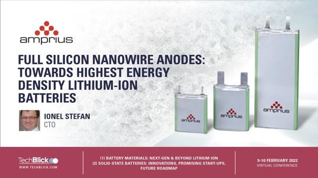
- Full silicon nanowire anodes: towards highest energy density Lithium-ion batteries
Speaker: Ionel Stefan | Company: Amprius | Date: 9-10 Feb 2022 | Full Presentation The silicon nanowire anode technology addresses silicon swelling by enabling silicon to expand and contract internally, in a very robust mechanical structure. As a result, over 1200 Wh/L and 450 Wh/kg levels of energy density were achieved in lithium-ion cells with a cycle life in the hundreds of cycles and fast charging in under 10 minutes, enabling new devices and applications. Join TechBlick on an annual pass to join all live online conference or online version of onsite conference access library of on-demand talks (600 talks + PDFs) portfolio of expert led masterclass year-round platform https://www.techblick.com/ Our next battery-related event will take place on 15-16 FEB 2023, covering 1) Solid-State Batteries: Innovations, Promising Start-Ups, & Future Roadmap 2) Battery Materials: Next-Generation & Beyond Lithium Ion The speakers include: General Motors, Graphenix Development, Brookhaven National Laboratory, Fraunhofer IKTS, RWTH Aachen University, Lawrence Livermore National Laboratories, Meta Materials Inc, Skeleton Technologies, Solid State Battery Inc, Argonne National Laboratories, OneD Battery Sciences, VTT, Leyden Jar Technologies B.V., b-Science, Rho Motion, Wevo-Chemie, LiNA Energy, CNM Technologies, Ionblox, Empa, Zinc8 Energy Solutions, Avicenne Energy, Echiontech, South8 Technologies, Basquevolt, NanoXplore, Chasm, Li Metal, Sila Nanotechnologies, Quantumscape (tentative), Fraunhofer ISI, etc https://www.techblick.com/