Search Results
1063 results found with an empty search
- Additive and 3D Electronics: LIFT for high viscosity, gravure printing, micro-bump Printing, Cu in Si TOPcon PV, inkjet on 8.5-Gen glass, high viscosity IJP, laser additive process for RDLs, etc
In this newsletter you can learn about the latest advances in Additive, Sustainable, Hybrid and 3D Electronics! via the following highlighted short videos, each being less than 2min, saving you learning time. These are all key points and advances in the field, advancing the art and cutting-edge. LIFT: R2R Digital Printing of High Viscosity Materials | Coatema How does Gravure Printing work in Printed Electronics? | Komori How to print micro bumps in a single step for semiconductor electronic packaging? | Hummink Can copper paste be used in Si TOPCon solar cell metal lisation to reduce silver consumption per cell and per watt ? | ISC Konstanz and Copprint How an actual inkjet printer prints functional and optoelectrical materials on a HUGE 8.5-Gen (2200 x 2500 mm2) display glass? | Kateeva Can we inkjet print screen printable and high viscosity pastes? | Quantica Laser-based additive electronics to simplify the RDL metallization process | Akoneer Time To Explore The World of Additive, Sustainable, Hybrid and 3D Electronics! Join the Electronics RESHAPED USA conference and exhibition in Boston (11 & 12 June) - Where the global Additive and 3D Electronics industry connects. Explore & RESHAPE The Future of Electronics NOW R2R Digital Printing of High Viscosity Materials? This is where inkjet struggled due to requirement for low viscosity inks and also nozzle clogging. LIFT can be a solution enabling R2R digital printing of materials with a range of viscosity levels, finally addressing a key industry limitation? Here in this short video Thomas Kolbusch from Coatema explains how R2R LIFT process works. This is a great explanation so we recommend watching it Video length: 1.5 min How does Gravure Printing work in Printed Electronics? Ever wondered how gravure printing actually works - especially in printed electronics? Hear Doug Schardt from Komori Corporation give a concise 2-min explanation of this wonderful process able to achieve very fine feature with all manners of inks, resists, etc at great scale and throughput. Video length: 2min How to print micro bumps in a single step for semiconductor electronic packaging? High Precision Capillary Printing (HPCaP) developed by Hummink enables the ability to print in a single step micro-bumps with ability to control diameter and aspect ratio. This capability enables amazing applications in semiconducting packaging. In particular, in laboratory and prototyping settings, this can accelerate the development process despite the actual printing step being relatively slow, since it eliminates many process steps. Video length: 1.2min Can copper paste be used in Si TOPCon solar cell metallisation to reduce silver consumption per cell and per watt? If silver consumption per solar wafer remains unchanged, silver shortages will limit the growth of the photovoltaic industry. It is thus vital to switch away from silver or reduce silver consumption. But adding printed copper with the right performance and reliability has been difficult to achieve and demonstrate. Here, ISC Konstanz has demonstrated that YES one CAN use indeed Cu paste with excellent performance AND high stability!! Here you can see the results from Ag consumption has been reduced from 126 mg to 60 mg (with additional of 97mg of Cu as bus bars) with same or higher performance. Furthermore, the solar cells are stabe passing • 3x IEC @ TCT (600 cycles) requirements passed without considerable degradation • 2x IEC @ DHT (2000h) requirements passed without considerable degradation • 3x IEC @ DHT (3000h) requirements passed without any degradation by the group with the encapsulation material EVA Video length: 1.2min How an actual inkjet printer prints functional and optoelectrical materials on a HUGE 8.5-Gen (2200 x 2500 mm2) display glass? Inkjet in printed electronics is often a small desktop machine throwing up the question can it ever be scaled up to huge areas. Here you can see see that yes it can. This is an example of area printing but still a great demonstrator. This video by Kateeva shows this beast of a machine and wonderful engineering in action demonstrating the inkjet can be truly scaled in additive and printed electronics Video length: 30s Can we inkjet print screen printable pastes? Inkjet has this major limitation of not being able to print high viscosity or even mid viscosity pastes. This limitation has truly held back inkjet in the world of additive and printed electronics. Quantica has developed a printer head that could enable direct inkjet printing of high viscosity pastes. This could be a game changer provided some challenges are addressed. Learn more here including about some of the challenges such as drying of paste during print at elevated temperature. Video length: 1.3min Can mask-less Additive Electronics simplify the RDL metallization process (both via and conductor layers) reducing number of process steps from ca. 11 down to 2-4 without any masks? This would be a superb achievement? Tadas Kildušis explains how SSAIL (Selective Surface Activation Induced by Laser) process (PI coat, laser pattern, activate, plate) can achieve this
- TechBlick Insights: Shear thinning, printed MCUs on PET, Ultrafine metal mesh films, perovskite solar vs Si solar, perovskite stability, microdispensed QDs for microLEDs, and more
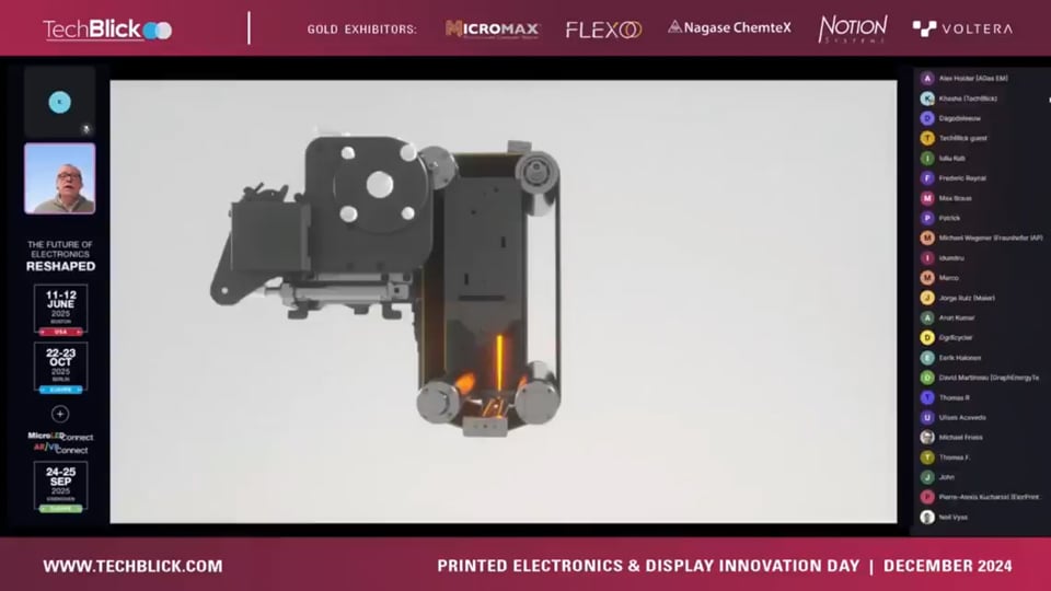
In this newsletter we cover the following Shear thinning of jetted solder and glue for assembly Fully printed double sided MCU on PET substrates? Ultrafine Cu mesh for transparent conductive films for touch, heating, security, etc film applications? Perovskite solar panels outperform the current silicon-based commercial panels, but what about cost? Perovskite solar panels are highly promising not just for utility-grade, but also for indoor light harvesting. Perovskite encapsulation for enhanced stability Microdispensing quantum dots for color conversion How will perovskite panels perform in the 'real world'? We cover these points by sharing short (1min or so) handpicked snippets from their live recent talks at TechBlick, Future of Electronics RESHAPED and Perovskite Connect conferences and exhibitions Join us at TechBlick’s Future of Electronics RESHAPED conference and exhibitions in Berlin on 22 and 23 OCT 2025. This is the global home of the additive, printed, 3D hybrid and sustainable electronics, bringing the entire value chain together, from innovators to suppliers and end users. This year as a special theme we will also collocate Perovskite Connect alongside the same show Explore program here now: The Future of Electronics RESHAPED Shear thinning of jetted solder and glue for assembly Shear thinning is one of the most important physical phenomena in jetting - or in fact in all of printed electronics! This is the physical mechanism on which much of the printed electronics industry relies! Here Irving Rodriguez from Essemtec explains this behaviour for jetting of solder as well as structural glue, showing how the shear rate increase in the jetting head leads to a drop a significant drop in viscosity Eric Wolf Cancalon Pierre-Jean (PJ) Mirko Cygon Fully printed double sided MCU on PET substrates? Lina Kadura from CEA-Liten presented at TechBlick Innovation Day in April 2025, showing a full printed double sided MCU PCB with 4 metal layers and 100+ through vias, accommodating over 40 SMT (400um MCU pitch). This is an incredible achievement showing that printed PCBs can lead to complex mullti-layer fully functional electronic PCBs for complex systems, showing that PCBs can be printed leading to greener solutions at lower cost? Ultrafine Cu mesh for transparent conductive films for touch, heating, security, etc film applications? Here Jonathan Chang from Panasonic North America explained at the TechBlick Future of Electronics SHOW USA (Boston, 2025) how they R2R form these films and what the key properties are. Fist the grooves are embossed into PET or PEC later and then the Cu mesh is formed. The mesh has 2um linewidth and is embedded within the film, yielding a smooth surface. The pattern is customised and the R2R process can do top and bottom layers at the same time giving rise to double sided films Perovskite solar panels outperform the current silicon-based commercial panels, but what about cost? In April 2025, during our Perovskite Innovation Day, Utmolight's co-founder Jesse Zheng said that while perovskites are not competitive yet, there are encouraging signs, and with a 10 GW factory, the company could reach cost parity with silicon. Perovskite solar panels are highly promising not just for utility-grade, but also for indoor light harvesting. In January 2024, during our Future of PV event, Halocell's Emanuele Calabró showed the superior performance of indoor light harvesting with its panels. Perovskite encapsulation for enhanced stability One of the key challenges that the perovskite industry still faces is the stability of lifetime of perovskite solar panels. In April 2025, during our Perovskite Innovation Day, Intellivation's Robert Malay introduced the company's encapsulation solutions, and discussed the challenges facing perovskite solar panel makers. Microdispensing quantum dots for color conversion XTPL developed a unique printing technology that offers high-performance and high precision material deposition, with several possible applications in the display industry. In December 2024, during our Display Innovation Day, XTPL presented their solution for micro bump deposition, and also presented a demonstration of QD deposition for microLED color conversion, a collaboration project with X-Display. Perovskite materials and exciting researchers and developers all over the world, as the industry is on the verge of mass commercialization starting with solar panels. In April 2025, during our Perovskite Innovation Day, Noctiluca's Łukasz Sytniewski explained why the company identified the perovskite solar industry as the key next market for the company, and detailed its new material R&D activities. How will perovskite panels perform in the 'real world'? Perovskite solar panels are highly promising, but people still wonder just how perovskite panels will perform in the 'real world'. In April 2025, during our Perovskite Innovation Day, Microquanta's Yang Chen details the latest performance of the company's perovskite panels - showing how they generate more electricity than silicon in harsh environments.
- VueReal | Unlocking MicroLED’s Potential: Why Reference Design Kits Are the Key to Mass Adoption
Brad Martin , VueReal | bmartin@vuereal.com MicroLEDs promise to reshape the future of displays and lighting - with higher brightness, lower power consumption, and longer lifespans than OLEDs. But for most innovators, that promise has remained just out of reach. Not due to lack of ideas or demand, but because of one persistent barrier: access. That’s now starting to change, thanks to the arrival of Reference Design Kits (RDKs): pre-integrated microLED modules that empower engineers, designers, and developers to prototype and experiment - without custom fabrication, high-volume commitments, or massive investment. By dramatically lowering the barrier to entry and leveraging flexible manufacturing methods, RDKs are unlocking a new era of innovation - accelerating both the pace of discovery and the path to mass adoption. We are Exhibiting! Visit our booth at the MicroLED Connect & AR/VR Connect in Eindhoven on 24-25 September 2025 The Real Bottleneck: Access, Not Imagination Unlike OLED panels - which are widely available for prototyping and development - microLEDs have historically been locked behind technical and supply chain hurdles. Most companies simply can’t get their hands on the technology. Traditional microLED manufacturing typically requires highly specialized equipment, high-volume commitments, and extensive engineering integration, putting it out of reach for the majority of companies. Even those who want to explore microLEDs in earnest are left to imagine what is possible rather than test, iterate, and build. This creates a fundamental mismatch between the potential of microLED and the ability of teams to work with it. A Shift Toward Flexible Manufacturing That dynamic is now beginning to change. Advances in high-precision transfer technologies - such as MicroSolid Printing - have introduced a new manufacturing model, one that supports high, medium, and low volume production without the need for dedicated fabrication facilities. With these processes, microLED modules can be produced flexibly, whether for single prototypes, pilot runs, or limited product lines. The result is lower capital expenditure, faster iteration, and greater accessibility for engineering and product teams of all sizes. Crucially, this unlocks the ability to offer microLED technology as a modular, off-the-shelf component: the Reference Design Kit. Reference Design Kits: The Bridge Between Promise and Product RDKs mark a major shift in how companies interact with microLED technology. Rather than needing to co-develop complex custom solutions from scratch, product teams can now acquire pre-built modules - complete with drive electronics, integration documentation, and support - to start experimenting immediately. These kits serve two essential purposes: Proof of Feasibility : RDKs demonstrate that microLED mass transfer and integration are not just theoretical - they’re commercially viable today. Platform for Innovation : RDKs empower teams to explore use cases, iterate quickly, and build proofs of concept in-house without large development contracts or IP entanglements. Reference Design Kits Bringing the Ecosystem to Life The arrival of accessible RDKs is catalyzing a new wave of ecosystem development across the semiconductor and display industries. OEMs, integrators, and supply chain partners can now collaborate on real prototypes, share feedback, and accelerate the learning curve for microLED integration. This collaborative environment not only speeds up product development but also helps establish new standards, best practices, and supply relationships - reshaping the value chain for next-generation displays and lighting. From “What If” to “What’s Next” Until recently, microLED Reference Design Kits (RDKs) simply did not exist. Now, with the first commercially available kits on the market, engineers and designers finally have a way to experiment with real, working microLED modules. The result: immediate momentum across a wide range of industries. Among the concepts generating early excitement: Ultra-Thin Automotive Lighting : Sleek, bright taillights and signal indicators that offer new levels of design flexibility. Transparent Steering Wheel or Windshield Displays : See-through displays that deliver information without obstructing a driver’s view. Advanced Puddle Lighting and Side-Mirror Signals : Compact, high-brightness modules that open the door to new safety and communication features. AR/VR Microdisplays : Ultra-bright, high-resolution microdisplays for next-generation headsets. Laminated Glass Displays : Embedded microLEDs within structural glass for automotive, architectural, and other applications. Innovations in auto with microLED These are just a few of the applications already under exploration. The real power of RDKs lies in the countless other ideas they will unlock - many of which will emerge once developers can experiment directly, without barriers. To capitalize on this shift, forward-looking companies should: Foster Cross-Functional Exploration : Bring together hardware, UX, and product teams to brainstorm and prototype with RDKs. Embrace Rapid Iteration : Use RDKs to test ideas early and often, accelerating learning and reducing development risk. Codevelop with your RDK Manufacturer : Offer feedback, request features, and participate in the co-creation of future modules and form factors. The Road Ahead The mass adoption of microLEDs is no longer a distant promise. With RDKs enabled by flexible, fab-free manufacturing models, access is now democratized. The technology is moving out of the lab and into the hands of the innovators who will shape its future. This ecosystem-driven approach will not only accelerate product launches but also foster new collaborations and standards across the industry. As microLED technology becomes truly accessible, expect a radical transformation in how displays and lighting are conceived and delivered across markets. We are Exhibiting! Visit our booth at the MicroLED Connect & AR/VR Connect in Eindhoven on 24-25 September 2025 Sidebar: What is MicroSolid Printing? MicroSolid Printing is a high-precision, additive mass transfer process that enables the rapid and flexible assembly of microLED arrays onto a variety of substrates. Unlike traditional methods that require dedicated fabrication facilities and high-volume runs, MicroSolid Printing also supports low- to medium-volume production - allowing manufacturers to deliver microLED modules in any quantity, from single prototypes to pilot runs. This process dramatically lowers capital expenditure and accelerates product development cycles, making microLED technology accessible to a much broader range of innovators. What to expect at the MicroLED Connect & AR/VR Connect event in Eindhoven on 24-25 September 2025?
- Developing a Custom Carbon Ink for Printing a Variable Resistor on PET
Custom resistive inks are formulated with carbon, metal, or hybrid particles, along with binders and solvents, to support applications in dimmers, sensors, and potentiometers. Their resistivity can be adjusted through particle concentration or trace geometry while balancing viscosity and adhesion. Contact: sales@voltera.io or +1 888-381-3332 ext: 1 MATERIALS USED Carbon black Polyvinylpyrrolidone (PVP) 2-(2-Butoxyethoxy)ethyl acetate Ethanol Voltera Conductor 3 silver ink ACI FS0142 flexible silver Ink Solder wire SUBSTRATES USED Polyethylene terephthalate (PET) 2" × 3" FR1 board TOOLS AND ACCESSORIES NOVA materials dispensing system V-One PCB printer 150 µm Subrex nozzle Nordson EFD 7018333 dispensing tip Voltera disposable nozzle Dual asymmetric centrifugal mixer Magnetic stirrer Bambu X1 Carbon 3D printer We are Exhibiting! Visit our booth at the TechBlick Berlin on 22-23 October 2025 Project overview Purpose In this project, we demonstrate the development of a carbon resistive ink through testing different ink formulations and validating the performance through a potentiometer and an LED circuit. Design We divided the design into four parts: Developing the carbon resistive ink Printing the potentiometer circuit Printing the LED circuit 3D printing the enclosure with a sliding wiper Desired outcome The goal was to develop an ink with great printability, which, for this project, we measured by viscosity (between 1,000–10,000 cPs, compatible with direct ink writing and screen printing ). We also aimed to achieve excellent adhesion to the substrate, with no flaking or cracking after curing at 90°C for 5 minutes. In addition, the ink should support a potentiometer to function properly, which means the resistance range should fall between 600 Ω to 6000 Ω. Functionality When connected to the LED dimmer board (powered by a 9V battery), sliding the wiper altered the potentiometer’s resistance, dimming or brightening three LEDs. Resistivity was tunable by adjusting carbon concentration, curing time and temperature, or printing thicker or shorter traces. While this formulation served as a functional prototype, higher carbon loadings (up to 20%) could be explored for enhanced conductivity, though viscosity adjustments would be necessary to maintain printability. Users can also change resistance by modifying the size of the conductive pad. Developing the carbon resistive ink* The development of custom functional inks, whether conductive, dielectric, resistive, or semiconducting, requires balancing particle loading, solvent compatibility, and binder selection to achieve target electrical and mechanical properties. While conductive inks rely on metallic particles like silver for low resistivity, resistive inks prioritize tunable compositions. Guided by these principles, we formulated a carbon-based resistive ink using carbon black for its cost-effectiveness and moderate conductivity, paired with PVP as a binder to enhance particle dispersion and substrate adhesion. The solvent blend, 2-(2-butoxyethoxy)ethyl acetate and ethanol, balanced evaporation rates and ink stability, critical for nozzle performance and film uniformity. Our iterative testing refined these ratios for compatibility with NOVA and the intended application. Carbon resistive ink developed by Voltera’s Applications team We started by dissolving 1.04 g of PVP into 4.88 g of ethanol using a magnetic stirrer at 1,500 rpm for 15 minutes. We then added 0.48 g of carbon black to the PVP-ethanol solution to minimize airborne particles, followed by the dropwise incorporation of 1.6 g of 2-(2-butoxyethoxy)ethyl acetate. We stirred the mixture for an additional 15 minutes under parafilm to prevent solvent evaporation, which resulted in a stable, homogenous ink. The final composition included 13% PVP as a binder, 6% carbon black for conductivity, 20% 2-(2-butoxyethoxy)ethyl acetate as a solvent, and 61% ethanol to stabilize the dispersion. This combination achieved a viscosity of about 1,500 cps, enabling smooth dispensing through the Nordson EFD 7018333 dispensing tip with an inner diameter of 250 µm. Final ink formulation** * Follow the guidelines in the safety data sheet when handling the carbon black powder. ** The formulation in the table is for an 8 g resistive ink and is scalable using the provided weight percentages. Printing the potentiometer circuit This circuit consists of two layers: Bottom conductive layer (in blue): Includes silver traces for solderable contacts, as well as a conductive pad to be glued onto the wiper of the potentiometer. Sliding the wiper up and down alters the carbon resistor’s effective length and changes the resistance of the circuit. Top resistive layer (in red): Carbon traces for the resistive element Potentiometer circuit design Bottom conductive layer NOVA settings, bottom conductive layer Bottom conductive layer, print result Top resistive layer NOVA settings, top resistive layer Final print The wiper of the potentiometer Printing the LED dimmer circuit This circuit was designed to visually demonstrate resistance changes by linking three LEDs to the potentiometer. Silver traces printed on an FR1 substrate formed conductive pathways, connecting the 9V power input to the potentiometer and LEDs. LED circuit design Once the circuit was cured, we manually placed and soldered the LEDs and reflowed the solder paste on V-One’s heated bed. The LED circuit board, soldered Printing the enclosure To house the potentiometer, we designed and 3D-printed a custom enclosure using PLA filament. The enclosure features a built-in sliding wiper mechanism for adjusting resistance and a compartment to securely hold the circuit components. After fabricating the enclosure, we cut the potentiometer circuit from the PET sheet and carefully taped it into the enclosure. Next, we soldered wires to the silver pads on the circuit to establish robust electrical connections. We then taped the conductive pad onto the wiper to ensure reliable contact with the resistive layer. After placing the wiper inside the enclosure, we twisted it 90 degrees to lock it into place. Finally, we connected the potentiometer to the LED dimmer circuit, which enabled real-time resistance adjustments for LED brightness control. The potentiometer circuit in the enclosure We are Exhibiting! Visit our booth at the TechBlick event on 22-23 October in Berlin Challenges and advice Clogging the nozzle During initial ink formulation trials, the carbon black particles aggregated in the solvent, which caused nozzle clogs and led to incomplete traces. After some investigation, we realized that the issue stemmed from insufficient dispersion stability — carbon particles settled unevenly in the solvent, forming dense clusters that blocked the nozzle. To address this, we introduced PVP as a dispersant and binder. We also adjusted the solvent ratio, reducing the volatile 2-(2-butoxyethoxy)ethyl acetate and increasing ethanol to improve particle suspension. Additionally, we recommend using a dual asymmetric centrifugal mixer to ensure homogeneous ink mixing. Lastly, we recommend using larger nozzles for particle-laden formulations to reduce shear stress during dispensing, as evidenced by better print results produced by the 330 µm nozzle, compared to the 200 µm nozzle. Conclusion As our first custom ink project, the bulk of work involved was iterating on ink formulation, trying to find the balance between printability and functionality. Using NOVA , we validated a new material in less than a month and created a repeatable process for developing carbon resistive ink. NOVA enabled our materials R&D process by allowing us to get immediate feedback on printability, iterate formulations right on our benchtop, and create novel electronics. If you’re interested in our other projects involving novel inks, take a look at: Printing ECG Electrodes with Biocompatible Gold Ink on TPU Printing an RFID Tag with Copper Ink on Paper Printing Electroluminescent Ink on Paper and PET Want to be notified when we post new white papers? Sign up for our newsletter . We are Exhibiting in Berlin. Visit our booth at the TechBlick event on 22-23 October 2025 in Berlin
- Voltera | Printing a Control Board for a Line Following Robot with Silver Ink on FR1
Prototyping robotics offers great potential in electronics education, providing a fun way to learn about sensors and motion control. Building a line-following robot can be both educational and practical, with applications in automated delivery systems and robot racing competitions. Contact: sales@voltera.io or +1 888-381-3332 ext: 1 MATERIALS USED Voltera Conductor 3 silver ink Voltera T4 solder paste Voltera solder wire SUBSTRATES USED FR1 board TOOLS AND ACCESSORIES V-One PCB printer Bambu Lab 3D printer Nordson EFD 7018395 dispensing tip Walfront infrared proximity sensors Texas Instruments L293DNE motor driver Texas Instruments NE555DR timers LEDs Rivets We are Exhibiting! Visit our booth at the TechBlick Berlin on 22-23 October 2025 Project overview Purpose The goal of this project was to prototype a circuit board that controls a line-following robot, using a simple design that could be used to teach electronics in a hands-on way. Design For the control board, we separated the ground traces and other signal traces on opposite sides of the FR1 board, with through-holes to mount key components like the 16-pin L293DNE motor driver. These through-holes also serve to accommodate other components such as LEDs, infrared proximity sensors, and motors, which could not be surface-mounted due to their size and functional requirements. Figure 1: Circuit design We divided the robot’s main body into small parts and printed them with a 3D printer. Desired outcome Once connected to power, a 9V battery, the assembled robot should be able to distinguish its designated paths from the background and navigate along the paths, making turns as needed. Functionality By using infrared proximity sensors, motors, and a motor driver, our design enabled the robot to move along the yellow tape on the black floor and navigate corners, all without relying on a microcontroller or onboard code, which would have introduced unnecessary complexity. For the purpose of this project, we did not require a specific travel speed. However, the design can be customized for other activities, such as robot racing or obstacle avoidance challenges by reducing the overall weight of the robot, adjusting the configuration of sensors, or choosing high speed rated motors. Printing the control board Printing the front side Before dispensing the silver ink, we drilled 39 through-holes with a diameter of 1.6 mm on the FR1 board using V-One. Figure 2: Through-holes drilled with a V-One PCB printer On the front side of the board, two infrared proximity sensors detect the paths and send signals to the motor driver, which controls the robot's movement by turning the motors on or off. Figure 3: Schematic for the control board, front side Figure 4: V-One dispensing settings Printing the back side The back side of the board consists of traces that connect to the ground pins of the components and complete the circuit. Figure 5: Schematic for the control board, back side Post-processing the control board. When both sides were complete, we inserted rivets into the through-holes and dispensed solder paste for resistors and the NE555 timer using V-One’s built-in solder paste dispensing workflow. We then populated the components and manually soldered the motor driver, capacitor, motors, infrared proximity sensors, and LEDs. Figure 6: Control board with components 3D printing the main body To house the control board and serve as the robot’s movement platform, we designed a main body divided into four parts. These parts were 3D printed using PLA filament: Two wheels Two motor brackets A case A lid Figure 7: Design of the main body We then put the control board into the case and assembled the parts. We are Exhibiting! Visit our booth at the TechBlick event on 22-23 October in Berlin Challenges and advice Soldering issues Conductive ink, when applied to FR1, can sometimes adhere less robustly compared to traditional copper traces on a PCB. This makes it prone to being lifted off the board during soldering if excessive heat, pressure, or mechanical stress is applied. To improve solderability, we lowered the curing temperature of the ink. This adjustment enhanced wettability, allowing solder to adhere more effectively to conductive pads, especially for sensitive connections and larger components. Conclusion Through this project, we developed a line-following robot controlled by a double-sided PCB, using a relatively simple design and readily accessible components. This highlights the feasibility of incorporating advanced robotics and electronics concepts into educational programs. Depending on the students' skill levels and the intended applications the design can be adjusted to make it more or less challenging. If you’re interested in exploring other PCB prototyping projects we have completed, take a look at: Printing a Flexible PCB with Silver Ink on PET Dispensing Solder Paste on Factory Fabricated PCBs Printing Strain Gauges on TPU laminated on a Glove for Remote Hand Control We are Exhibiting in Berlin. Visit our booth at the TechBlick event on 22-23 October 2025 in Berlin
- MicroLED and AR/VR Display Insights: Digital signage, stable QDs, red GaN, smart glasses, VC funding and More
MicroLED Displays for Digital Signage Insights from JCDecaux’s R&D Director, Thomas Morel, on next-generation microLED technologies for large-scale signage and outdoor displays. Quantum Dot Stability for MicroLED Color Conversion QNA Technology presents UV LED-based QD color conversion with enhanced stability for microLED applications. Advancements in Red GaN MicroLED Production Prof. Daisuke Lida (KAUST) discusses cutting-edge techniques to achieve high-efficiency red GaN microLEDs, addressing production and cost challenges. Key Features of Smart Glasses: Fashion & Vision Google AR Director Bernard Kress highlights fashion and prescription lens integration as the top factors shaping the future of AR smart glasses. Impact of Outer Shell on Cadmium Sulfide QD Performance Fraunhofer IAP’s Dr. Manuel Gensler explains how the outer shell diameter affects the optical and electronic performance of CdS quantum dots. VC Funding & Challenges for Semiconductor Startups Cyril Vančura (imec.xpand VC) shares why “fast fail” strategies don’t work for microLED and semiconductor startups, and how to secure sustainable growth. We cover these topics through short (1-minute) handpicked snippets from recent live talks at TechBlick, at Future of Electronics RESHAPED and MicroLED Connect + AR/VR Connect conferences and exhibition series. MicroLEDs for Digital Signage? JCDecaux a global leader in digital signage and has been using novel cutting-edge technologies and business models for many years. Hear JCDecaux's R&D Directory, Thomas Morel explain the company's views on next-generation microLED displays for signage applications. Are quantum dots stable enough for microLED color conversation Quantum Dots are highly promising for color conversion in microLED displays. But the stability of the material is still a technical challenge. In September 2024, during our flagship 2024 MicroLED-Connect event, QNA Technology introduced its unique UV LED color conversion QD technology, and showed the impressive stability its QDs offer. What is the state of the art in red GaN MicroLED production Producing high-efficiency red microLEDs is one of the major challenges towards efficient and low-cost microLED displays. During MicroLED Connect 2024, Prof. Daisuke Lida, from KAUST, explained the state-of-the-art in red microLED production and the latest research at KAUST. What are the most important features of smart glasses? In September 2024, during our flagship 2024 MicroLED Connect + AR/VR Connect event, Google's AR Director Bernard Kress gave an excellent talk about the future of smart glasses. Interestingly, Bernard says that the two most important considerations are fashion, and prescription vision integration! Impact of outer shell on performance of Cadmium Sulfide QDs During MicroLED Connect 2024, Dr. Manuel Gensler from the Fraunhofer IAP explained how the performance changes when you increase the diameter of the outer shell of Cadmium Sulfide Quantum Dots. Join MicroLED Connect and AR/VR Connect to stay updated on the latest microLED innovations and network with industry leaders—whether at our flagship onsite event, our annual series of virtual meetings, or through our extensive content library. Why fast fail is not an option for semiconductor startups. The MicroLED Industry is still at a very early stage, and there are many early stage companies and startups that develop microLED technologies. And these companies need funds... During MicroLED Connect 2024, Cyril Vančura , partner at imec.xpand VC gave excellent tips for early stage microLED startups. In this short video, you'll see Cryil explain why fast fail is not an option for semiconductor startups.
- Introducing the Perovskite Connect 2025 program: perovskite solar panels and novel materials
Perovskite Connect 2025 Conference and Exhibition | ECC, Berlin, Germany | 22 & 23 OCT 2025 | Co-located with Future of Electronics RESHAPED Europe 2025 Perovskite Connect 2025 is set to be the industry’s premier event, with a world-class agenda, exhibition and networking opportunities. Co-located with Europe’s leading printed electronics event, Perovskite-Connect will focus on the perovskite supply chain, solar applications, recent innovations, materials and processes. In this article we will introduce some of our speakers and themes at the event. You can explore the full agenda and event details here . Perovskite solar applications – utility solar is not the only game in town The main application for perovskite materials today, and the one that attracts most of the attention, is of course solar energy generation. While many companies focus on solar panels for utility – gird purposes, many companies are looking for alternative applications – such as indoor solar, agrivoltaics, building- and vehicle-integrated panels and more. At Perovskite-Connect, we will explore all of these themes! Here we show some of our planned talks that will focus on perovskite solar applications. At Perovskite Connect 2025, Microquanta , China-based leading perovskite solar panel developer, will discuss the commercial readiness of perovskite PVs for utility-grade solar, and will share lessons the company has learned through real-world deployment and industrial validation. Microquanta believes that perovskite PV is evolving into a commercially ready solar technology—poised not only to complement, but to surpass traditional silicon in key applications. UK-based tandem perovskite solar panel developer Oxford PV recently announced the world’s first commercial tandem perovskite-silicon panels. The company’s presentation at Perovskite-Connect will explore the rapid development and exceptional performance of perovskite-silicon tandems, highlighting recent advancements and charting the roadmap to further improvements. A particular emphasis will be placed on scaling and manufacturability. Perovskia develops high performance indoor and outdoor perovskite solar panels. The company will detail its unique perovskite production process, and the high customization it offers for its customers that seek to integrate high-performance solar panel into their products, without compromising on design. Finally, Swift Solar will give a lecture that details the company’s journey to develop a high-throughput manufacturing technique and improve its process reliability, in order to achieve consistently high yields. Swift Solar will also highlight its expanded testing infrastructure, designed to evaluate large volumes of devices over extended durations, and will present results from experimental studies. Perovskite materials innovations As the perovskite industry matures, there’s a growing demand to increase panel efficiency, reduce costs, increase lifetime and stability, and more. The design of novel perovskite stack materials is a key pillar of the industry’s effort to commercialize perovskite panels. At Perovskite-Connect 2025, Sofab Inks will discuss its effort to explore materials that can increase the performance of perovskite devices, and are also scalable for mass production. The company’s soluble ETL and HTL materials offer a solution for the industry that balances performance and manufacturability. Germany-based Karlsruhe Institute of Technology (KIT) will introduce its research into metallization and interconnection materials that can be processed at low temperatures. One of its key achievements is the TECC wire concept which uses round copper wires for cell interconnection. These polymer-coated wires offer good adhesion to the cell structure, high performance, low silver content and a gentle processing condition. Nano-C is also developing interface materials for single-junction and tandem perovskite panels. The company will discuss how its experience with fullerenes and fullerene derivatives has enabled it to develop novel electron transporting interface materials that allow for passivation and prevention of delamination, and will also discuss specific use cases of the materials and its industrial scale manufacturing of fullerenes and new generation fullerene derivatives . Finally, industrial adhesive developer DELO will explain why high-barrier encapsulants are essential for the protection of perovskite solar cells, and will demonstrate how it developed new adhesive solutions specifically designed for perovskite solar cells. Perovskite Connect 2025: time to reserve your ticket now! These are just a few sample themes from our exciting world-class agenda, that includes a range of solar panel makers, equipment manufacturers, process developers, researchers and more. Perovskite-Connect is co-located with The Future of Electronics Reshaped printed electronics event, a highly relevant conference with a focus on printed materials, processes and technologies. Perovskite Connect 2025 – the Exhibition The Perovskite-Connect exhibition is the key place where you can find partners across the entire value chain, including equipment manufacturers, material makers, solar panel makers and more.
- Join the Metallization and Interconnection Workshop for Solar Cells (MIW) as a TechBlick visitor
Please note that just before the TechBlick Future of Electronics RESHPAED and Perovskite Connect conference on 22 and 23 OCT 2025 in Berlin, the 13th edition of the renowned Metallization and Interconnection Workshop for Solar Cells (MIW) will take place in Berlin during the same week. This specialized workshop focuses on current and emerging approaches to the metallization and interconnection of solar cells, attracting over 120 experts from industry and academia worldwide. Over the course of two days, a series of scientific presentations—selected through a rigorous review process—will be delivered. A key feature of the workshop is its strong emphasis on discussing results and trends, making it equally valuable for both newcomers and seasoned professionals. TechBlick has entered into a partnership with MIW so that visitors to TechBlick receive a discount of EUR 120 on the admission price for the MIW workshop. Further information about the MIW workshop can be found at https://miworkshop.info/
- Additive and Green PCBs, Perovskite QD, Pick-and-Place for Flexible Hybrid Electronics, Nanscale printing, MicroLED Interconnects, Red GaNs, and more
In this newsletter we cover the following Is additive manufacturing of PCBs more environmentally friendly than traditional subtractive processes? | Lina Kadura from CEA-Liten Pick and place machines for Flexible Hybrid Electronics? | Irving Rodriquez, Essemtec Print nanoscale structures with varying or gradient material compositions? | Gauthier Briere, Atlant 3D Microdispensing in microLED interconnect production? | XTPl Can perovskite QDs be used as color conversion in microLED displays? | CEA Leti's Prof. François Templier How can the LED industry adapt to the needs of microLED displays? | ALLOS Semiconductor How will perovskite panels perform in the 'real world'? | Microquanta's Yang Chen Are microLEDs really more efficient than OLED displays? | UCSB, Prof. DenBaars We cover these points by sharing short (1min or so) handpicked snippets from their live recent talks at TechBlick and MicroLED Connect conferences and exhibitions Is additive manufacturing of PCBs more environmentally friendly than traditional subtractive processes? Lina Kadura from CEA-Liten presented at TechBlick Innovation Day in April 2025, showing that life cycle analysis (LCAs) demonstrate that the GWP index - the Global Warming Potential - can be reduced by 50% just by switching to additive, without even changing substrates away from FR5! This clearly demonstrates that additive electronics and printed electronics can make electronics more sustainable and greener Pick and place machines for Flexible Hybrid Electronics? Irving Rodriguez from Essemtec presented recently at the TechBlick Innovation Day, showcasing their all-in-one system able to achieve pick-and-place, solder as well as glue jetting a single machine with a footprint less than 1 square meter and with the ability to change the printing value in less than 30 seconds. Here you can also see the machine for flexible hybrid electronics where the special vacuum table holds down the foil (substrate), allowing the placement of 0.1 or 0.2 mm up to 109 mm components on flexible hybrid electronics! The pick and place is often a critical challenge in realising printed hybrid systems and this machine offers a powerful solution. Print nanoscale structures with varying or gradient material compositions? Direct Atomic Layer Processing (DALP) can enable multi-material direct micron- or nano-scale atomic layer deposition or printing! Here the lateral feature size is determined by the microreactor, while the vertical feature size is controlled by the ALD process itself. This allows for highly controlled and repeatable patterning of materials like metals, oxides, and nitrides. Here Gauthier Briere, formerly at Atlant3D, showcases a unique ability of this technology, namely the ability to print ultrafine structure with varying metal gradients / material compositions and heights. This is an ability that almost no other method can match Microdispensing in microLED interconnect production? Tiled microLED displays usually use electrodes deposited on the edges of the tiles, as these need to connect seamlessly. In December 2024, during our Display Innovation Day, XTPL presented their solution for high-performance Edge-Type conductive interconnect deposition. Here 10um wide lines with 15um spacing using highly conductive and dense silver paste is printed directly around the edges connecting the front and back Can perovskite QDs be used as color conversion in microLED displays? Perovskite quantum dots are highly promising materials, with excellent potential in display applications, especially for color conversion in microLED displays. In December 2024, during our Display Innovation Day, CEA Leti's Prof. François Templier presented the latest research results, including their ability to achieve densities of 1 micron or even less, thanks to the perovskite materials. How can the LED industry adapt to the needs of microLED displays? The LED industry is not optimized for producing microLED for display applications. What kind of changes will the industry adopt in order to mass produce low-cost and high-performance microLED chips? In September 2024, during our flagship 2024 MicroLED-Connect event, ALLOS Semiconductor explained the required manufacturing systems for successful microLED production, and gave an introduction to the company's GaN-On-Silicon 300 mm production technology an d expertise. Are microLEDs really more efficient than OLED displays? And how will vertically-stacked LEDs increase performance? In September 2024, during MicroLED-Connect's flagship event in Eindhoven, UCSB's Prof. DenBaars presented the latest state-of-the-art LED research results, detailed the lab's work on tunnel-junction technology that enables single-chip full color solutions, and explained why native red microLEDs are still a big challenge. How will perovskite panels perform in the 'real world'? Perovskite solar panels are highly promising, but people still wonder just how perovskite panels will perform in the 'real world'. In April 2025, during our Perovskite Innovation Day, Microquanta's Yang Chen details the latest performance of the company's perovskite panels - showing how they generate more electricity than silicon in harsh environments.
- The Future of Electronics RESHAPED conference and exhibition: Program update (22 & 23 OCT 2025, Berlin)
The most important conference and exhibition worldwide dedicated to printed electroncis, additive electronics, sustainable electronics, wearable electronics, stretchable electronics, soft electronics, textile electronics and more https://www.techblick.com/electronicsreshaped Discover the Future of Additive, Printed, Sustainable, Hybrid, Wearable & 3D Electronics 🔷100 onsite talks 🔷90+ exhibitors 🔷12 masterclasses 🔷3 tours 🔷600+ participants Join us at Electronics RESHAPED in Berlin on 22 and 23 OCT 2025 - the flagship global meeting point for applied research and industry. Join the movement. Explore & RESHAPE the Future of Electronics – NOW! World-class agenda with 100 onsite talks - Breakthroughs reshaping tomorrow—on stage at TechBlick in Berlin! Incredible agenda including 100 talks organised in 4 parallel tracks from across the entire technology spectrum and across the globe. The agenda features Toyota, Lockheed Martin, Valeo, Antolin, Sato Global, GE Aerospace, Fuji, Panasonic, Kodak and many other incredible large and small companies as well as research centres. No other event worldwide offers such a cutting-edge and comprehensive agenda as TechBlick events. Explore The Agenda NOW Incredible tradeshow with 90+ exhibitors What happening next is already on show here! Dynamic tradeshow floor featuring over 90 exhibitors from around the world, showcasing their latest innovations and products. This is an incredible opportunity to explore the state-of-the-art in the industry and applied research. More than 90% of the available spots are sold. Contacts us now if you wish to join as an exhibitor - tom@techblick.com Explore The Exhibition Floor NOW Unparallel networking - TechBlick is where all the key conversations take place! The show offers unparalleled networking in a great atmosphere during the entire event including the extended refreshment breaks. We provide coffee, lunch and beverages as well as drinks to keep everyone together the entire time. Indeed this show has a unique spirit! Explore The Exhibition Floor NOW
- Perovskite Connect Conference and Exhibition: Latest Program Update
The first ever conference and exhibition worldwide focused on perovskite industry Explore the cutting-edge technology, manufacturing advances, and real-world applications of perovskites 🔷First-ever show worldwide dedicated to perovskite industry 🔷World-class global agenda 🔷Vibrant exhibition 🔷Masterclasses and tours Join us at the Perovskite Connect in Berlin on 22 and 23 OCT 2025 - the flagship global meeting point for applied research and industry. Explore & RESHAPE the Future of Perovskites– NOW! Next Early Birds Discount Ends on 18 July 2025 World-class global agenda - The next perovskite breakthroughs unveiled at at Perovskite Connect in Berlin! Incredible curated agenda featuring all the key players, material and component innovations, and manufacturing advances - from across the world. Speakers include the likes of Microquanta, Oxford PV, Swift Solar, Beyond Silicon, Inc., Caelux Corporation, SparkNano, Helmholtz-Zentrum Berlin, Sofab Inks, CEA, Solaires Entreprises Inc, and many more. No other perovskite event worldwide will offer such an incredible global agenda focused on industry and applied research. Explore The Agenda NOW Next Early Birds Discount Ends on 18 July 2025 Dynamic tradeshow - Perovskite Connect - where the perovskite industry is on show The co-located exhibition floor showcases the depth and breadth of the global perovskite ecosystem featuring leading producers and pilot lines, material and equipment developers as well as applied research centres. The floorplan is shown below. The exhibition is co-located with the Future of Electronics RESHAPED conference and exhibition, featuring a total of over 90+ booths There is only ONE spot left in the Perovskite Connection exhibition section - contact khasha@techblick.com if you are interested. Explore The Exhibition Floor NOW Co-located with the Future of Electronics RESHAPED - Perovskite Connect - where the industry's defining conversations take place Perovskite Connect is part of the Future of Electronics RESHAPED show, offering full access to 100+ onsite talks, 90+ exhibitors and networking with over 600 participants from around the world over extended refreshment breaks and drinks receptions. Explore The Joint Program NOW Next Early Birds Discount Ends on 18 July 2025
- Roll-to-Roll Process to Transform the Creation of Flexible Printed Electronics in Healthcare | Linxens
Author : Sabine Kaced | sabine.kaced@linxens.com How can the Roll-to-Roll Process Transform the Creation of Flexible Printed Electronics in Healthcare? The healthcare industry is experiencing a revolution, driven by advancements in wearable devices and biosensors that monitor patients non-invasively and in real time. At the forefront of this transformation is the Roll-to-Roll (R2R) process, a manufacturing breakthrough that is reshaping how flexible printed electronics are created. Linxens Healthcare is leading the way in leveraging R2R technology and contract manufacturing capabilities to deliver cost-effective, scalable and precise solutions for innovative healthcare monitoring. Harnessing the power of Roll-to-Roll technology At Linxens Healthcare, we harness the power of the R2R process to produce cutting-edge electronic skin patches equipped with electrochemical sensors, integrated electronic components, and skin adhesives. With years of expertise in printed electronics and converting, Linxens Healthcare has established itself as a trusted partner for the development and manufacturing of flexible healthcare solutions. Inside the Roll-to-Roll Process: Driving Innovation in Healthcare R2R is a high-throughput manufacturing technique that involves the continuous processing of flexible substrates - such as plastic films, metal foils, or textiles - through various stages of printing, coating, and assembly. At Linxens Healthcare, we utilize advanced printing methods like screen printing, gravure printing, inkjet printing, and flexographic printing, to deposit functional inks onto the substrate with exceptional precision. We are Exhibiting! Visit our booth at the TechBlick event on 11-12 June 2025 in Boston . Our R2R workflow includes: Substrate Handling: Feeding flexible substrates through rollers for precise alignment and tension control. Layer Deposition: Printing conductive, dielectric, or active material layers using techniques tailored to the application’s requirements. Drying/Curing: Employing thermal or UV curing to solidify printed layers and achieve optimal conductivity and chemical properties. Lamination and Assembly: Integrating additional components, such as microchips, sensors, and adhesives, onto the substrate. Inspection and Testing: Ensuring every product meets the highest quality standards. Transforming Healthcare Applications Linxens Healthcare’s R2R capabilities enable the seamless integration of electrochemical sensors, electronic components, and medical-grade adhesives into flexible skin patches. These advancements create unparalleled opportunities to monitor vital signs including heart rate, respirations, hydration levels, blood glucose levels and more in real time, offering both patients and healthcare providers actionable insight. Key Advantages of Linxens Healthcare’s R2R technology Precision and Miniaturization Our R2R technology enables high-resolution printing of electrodes and interconnects, critical for accurate physiological signal detection. With advanced techniques like inkjet printing, we achieve nanometer-scale conductive patterns essential for compact and lightweight wearable designs. Material Compatibility Our expertise extends to working with a wide range of functional inks, including conductive silver and carbon, as well as bio-functional coatings. These materials are essential for creating durable and biocompatible electrochemical sensors that maintain performance standards in various medical environments Seamless Integration of Components Our R2R manufacturing process allows the integration of microelectronics, such as Bluetooth modules or near-field communication (NFC) chips, directly onto flexible substrates. This integration enhances device performance and supports wireless data transmission to smartphones or cloud platforms. Adhesive Application We apply medical-grade adhesives with precision, ensuring a secure and comfortable fit on the skin. This ensures optimal sensor performance and a positive user comfort in all applications. Scalability and Cost-Effectiveness Linxens Healthcare’s R2R process drastically reduces production time and costs, allowing us to efficiently scale from prototyping to mass production. This scalability enables us to meet the growing demand for wearable healthcare devices, making advanced monitoring technologies more accessible and affordable. Partner with Linxens Healthcare for Next-Generation Solutions Choosing to partner with Linxens Healthcare means gaining access to industry-leading expertise in printed electronics and contract manufacturing. Our approach includes: Enhanced Customization: From rapid prototyping to customized designs, we adapt solutions to specific healthcare applications and user needs. Scalability: Scale from prototyping to mass volume production in million range without compromising on quality. Reliability and Quality: Inline monitoring systems ensure our products meet stringent healthcare standards. Market Competitiveness: Mass-producing high-quality devices at lower costs helps our partners stay ahead in the market. Future Outlook: Shaping the Future of Healthcare Monitoring Linxens Healthcare’s R2R technology opens the way for the next generation of wearable healthcare solutions. From multi-parameter monitoring patches to real-time data transmission devices, we empower patients and healthcare providers with innovative tools. With a focus on materials innovation, advanced printing techniques, and automation, Linxens Healthcare is committed to transforming how vital signs are monitored and managed. Our expertise in printed electronics and contract manufacturing positions us as a leader in delivering high-performance solutions that redefine the healthcare experience. Partner with Linxens Healthcare today and experience the future of flexible printed electronics in healthcare. https://healthcare.linxens.com/ | LinkedIn Linxens Healthcare We are Exhibiting in Boston and in Berlin. Visit our booth at the TechBlick event on 11-12 June 2025 in Boston 22-23 October 2025 in Berlin