


10 December 2018
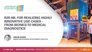
R2R-NIL for realizing highly innovative use cases – from bionics to medical diagnostics
Speaker: Gregor Scheipl | Company: Joanneum Research | Date: 24-Jun-22 | Full Presentation Imprint lithography is a versatile technology for the replication of micro- and nanostructures. It is widely used in high-tech areas such as optics, electronics, photovoltaics, sensor technology, in the medical field ("lab-on-chip") or in surface finishing. As a European pioneer, JOANNEUM RESEARCH Forschungsgesellschaft mbH operates a roll2roll (R2R) UV coating and imprinting system since 2010 and is developing and using resins that are biodegradable and thus sustainable. Required structures can be produced on a meter-per-minute scale, similar to newspaper printing. With a strong focus on the product, processes are developed and optimized for: (i) Environmentally friendly production of high-resolution conductive structural elements for organic electronics (fine conductor paths, nanoscale electrodes for organic transistors) (ii) Precise production of optical 2.5D structures for the management of light in films (coupling and decoupling, light conduction) for applications in photonics (iii) Large-scale realization of 3D-structured bionic surfaces and complex nanostructures that make effects from nature technically usable (shark skin, lotus effect, gecko effect, structural colors) (iv) Cost-effective production of complex microfluidic elements in foil as the basis of biosensors for lab-on-foil analysis systems (v) Continuous production of refined high-tech film surfaces for packaging, decor...
26 November 2018
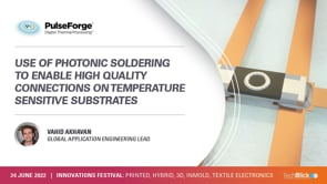
Use of Photonic Soldering to Enable High Quality Connections on Temperature Sensitive Substrates
Speaker: Vahid Akhavan | Company: PulseForge | Date: 24-Jun-22 | Full Presentation Many prototypes have been developed in the flexible hybrid electronic space that do not go to production due to poor longevity of the final design. One of the big challenges remains how to connect conventional component to a flexible architecture, while maintaining the expected longevity in the circuit. Anisotropic conductors are the current benchmarks for these devices, but their performance is lacking as compared to standard soldering processes. PulseForge has devised a new photonic soldering process that enables attachment using standard solder pastes onto components and substrates that cannot withstand the oven reflow temperatures. Photonic soldering utilizes high intensity flashes of visible light to achieve wide area heating with exceptional uniformity. Solder paste is heated to its liquidous temperature using radiative energy transfer, and light is converted to heat through optical absorption. This process is selective by exploiting selective absorptivity of active regions or with the aid of shadow masks. The optical flash can be modulated digitally, with high temporal resolution, to enable highly customizable temperature profiles, ranging from traditional to highly innovative. Photonic soldering is compatible with standard high temperature lead free solder alloys (e.g. SAC305) in combination with temperature-sensitive substrates (e.g. PET). The nonequilibrium nature of the heating proce...

12 November 2018
Established and new applications of printed e-paper displays
Speaker: Keith Morton | Company: Ynvisible | Date: 24-Jun-22 | Full Presentation Keith Morton, Ynvisible's VP of Sales & Marketing, will speak about established and new applications that are benefiting from their printed, ultra-low-power, and cost-effective e-paper technology. Join TechBlick on an annual pass to join all live online conference or online version of onsite conference access library of on-demand talks (600 talks + PDFs) portfolio of expert led masterclass year-round platform https://www.techblick.com/ And do NOT miss our flagship event in Berlin on 17-18 OCT 2023 focused on Reshaping the Future of Electronics. This event attracts 550-600 participants from all the world and offers a superb ambience and dynamic exhibition floor. To learn more visit https://www.techblick.com/electronicsreshaped To see feedback about previous event see https://www.techblick.com/events-agenda...
29 October 2018
Pad-printing Silver Inks – Example of 5G Antenna Applications
Speaker: Thibaut Soulestin | Company: Henkel AG & Co. KGaA | Date: 24-Jun-22 | Full Presentation Henkel is an industry-leading supplier of printed electronics materials and services. The broad Loctite portfolio of functional inks includes silver inks, carbon inks, silver/ silver chloride inks, dielectric inks, and other non-conductive inks as well. Due to Henkel’s extensive partnership network, we are uniquely situated to provide high-quality materials for a variety of printed electronics applications. Combining the trend of 3D electronics and increased connectivity, we recently developed a range of silver inks for pad-printing. This ink range enables the direct 3D-printing of 5G antenna on the smartphone frame. Join TechBlick on an annual pass to join all live online conference or online version of onsite conference access library of on-demand talks (600 talks + PDFs) portfolio of expert led masterclass year-round platform https://www.techblick.com/ And do NOT miss our flagship event in Berlin on 17-18 OCT 2023 focused on Reshaping the Future of Electronics. This event attracts 550-600 participants from all the world and offers a superb ambience and dynamic exhibition floor. To learn more visit https://www.techblick.com/electronicsreshaped To see feedback about previous event see https://www.techblick.com/events-agenda...
3 December 2018
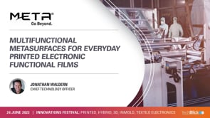
Multifunctional metasurfaces for everyday printed electronic functional films
Speaker: Jonathan Waldern | Company: META (Metamaterial) | Date: 24-Jun-22 | Full Presentation Meta Materials Inc. is developing discrete platform specific proprietary technologies for large-surface-area lithography, allowing the manufacture of nanostructures to be carried out in a cost-effective manner. Each platform employs a massively parallel patterning scheme, designed to be scalable to large areas of either rigid substrate materials and rolls of flexible films. In certain cases we use a phase-shift mask approach and in others, cast plasmonic printing – all allowing the creation of structures with feature sizes down to 50 nm. Join TechBlick on an annual pass to join all live online conference or online version of onsite conference access library of on-demand talks (600 talks + PDFs) portfolio of expert led masterclass year-round platform https://www.techblick.com/ And do NOT miss our flagship event in Berlin on 17-18 OCT 2023 focused on Reshaping the Future of Electronics. This event attracts 550-600 participants from all the world and offers a superb ambience and dynamic exhibition floor. To learn more visit https://www.techblick.com/electronicsreshaped To see feedback about previous event see https://www.techblick.com/events-agenda...
19 November 2018
Polyester film solutions from DTF meeting changing needs in flexible electronic markets
Speaker: Valentijn von Morgen | Company: DuPont Teijin Films UK Ltd | Date: 24-Jun-22 | Full Presentation Continued advances in the Flexible and Formable Electronics is driving the material suppliers such as DuPont Teijin Films to provide functionality to meet wide ranging demands for applications such as displays, TFT backplanes, energy harvesting and storage, sensors and Human Machine Interfaces. This talk will give a brief overview of DTF’s PET and PEN product range meeting wide ranging application needs. Thereby the focus will be on the recent progress made with the development of PEN substrates for extreme processing requirements, formable PETfilms for in-mold electronics, films with ultra clean and smooth surfaces for ultra barrier and high resolution structures and combining UV absorption, weather resistance or fire retardancy whilst also offering more sustainable solutions with the incorporation of recycled materials in the substrates. DTF has launched many films through collaborations with partners in the flexible electronic industry as our organisation is proving to be uniquely capable of offering customised and affordable polyester substrate solutions. Join TechBlick on an annual pass to join all live online conference or online version of onsite conference access library of on-demand talks (600 talks + PDFs) portfolio of expert led masterclass year-round platform https://www.techblick.com/ And do NOT miss our flagship event in Berlin on 17-18 OCT 2023 focused ...
5 November 2018
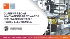
Current R&D at InnovationLab: Towards reflow-solderable hybrid electronics
Speaker: Meike Baumgarten | Company: InnovationLab GmbH | Date: 24-Jun-22 | Full Presentation What happens currently at InnovationLab? Insights into what iL’s R&D department researches on regarding hybrid and flexible electronics, along with interim results and next steps. This will be accompanied by the one or other novel development Join TechBlick on an annual pass to join all live online conference or online version of onsite conference access library of on-demand talks (600 talks + PDFs) portfolio of expert led masterclass year-round platform https://www.techblick.com/ And do NOT miss our flagship event in Berlin on 17-18 OCT 2023 focused on Reshaping the Future of Electronics. This event attracts 550-600 participants from all the world and offers a superb ambience and dynamic exhibition floor. To learn more visit https://www.techblick.com/electronicsreshaped To see feedback about previous event see https://www.techblick.com/events-agenda...
22 October 2018
Your copper nanoparticle production scale up
Speaker: Zachary J. Davis | Company: Danish Technological Institute | Date: 24-Jun-22 | Full Presentation Finding sustainable alternative conductive materials to silver is growing in demand. Copper is the next best conductive material, extremely abundant and much cheaper compared to silver and thus is a prime candidate moving forward. DTI has developed several micro and nano copper particles and has demonstrated industrial production of up to 10 kg per day. This talk will showcase the reactor technology DTI has developed, consisting of both a material synthesis reactor as well as filtration system, for automated production of micro/nanomaterials, for printed electronic application, as well as preliminary results for copper based inks produced using produced particles. Join TechBlick on an annual pass to join all live online conference or online version of onsite conference access library of on-demand talks (600 talks + PDFs) portfolio of expert led masterclass year-round platform https://www.techblick.com/ And do NOT miss our flagship event in Berlin on 17-18 OCT 2023 focused on Reshaping the Future of Electronics. This event attracts 550-600 participants from all the world and offers a superb ambience and dynamic exhibition floor. To learn more visit https://www.techblick.com/electronicsreshaped To see feedback about previous event see https://www.techblick.com/events-agenda...