


17 August 2022
Morphotonics | Cost-effective Large-area Roll-to-Plate Imprinting
Author: Erhan Ercan | erhan.ercan@morphotonics.com | Jan Matthijs ter Meulen | Kidong Lee Cost-effective mass manufacturing of nano/micron textures is needed to make life-enhancing products commonplace and affordable for consumers. Incorporating such structures via nanoimprinting in higher value-added products like sunlight-readable smartphones, immersive augmented reality glasses, and autonomous-driving-enabling LIDAR sensors will significantly improve our daily lives. Morphotonics, a Dutch nanotechnology company, develops and sells Roll-to-Plate (R2P) imprint technology & equipment. Our market-proven R2P imprint technology enables the mass-manufacturing of such nano/micron-size surface structures over extremely large areas. This leads to unprecedented cost advantages and radically improved products for our customers in the display, sensing, solar, and other deep technology sectors, where such manufacturing precision with cost-competitiveness is the prerequisite for mass-market entry. Morphotonics’ R2P imprint equipment can imprint on substrates with a width of up to 1100 mm (GEN5-size, 1100 x 1300mm2, as shown with Portis 1100 in Figure 1). The process of this R2P imprinting technique is schematically represented in Figure 2. The large area imprint capability enables the manufacturing of a larger number of smaller products in a single imprint step (‘product tiling’). The R2P process can imprint 5 to 20 times more products in comparison to the traditional wafer-scale ...

16 August 2022
Molecular inks for extreme shapes | Narrowband inkjettable phosphors | R2R sheets of GaNs...
Molecular inks for extreme shapes | Narrowband inkjettable phosphors | R2R sheets of GaNs| Silicone-based AgCl inks| Art of screen making | EMI Sheild House Keeping Note I: TechBlick is now putting together its agenda for its Innovation Showcase Day on 6 June 2022. Email khasha@TechBlick.com if you wish to present. In our last event we had nearly 600 live participants over a 4 hour period! Topics: In this edition, we will cover the following technologies: Molecular inks for extreme shapes | Narrowband inkjet printable phosphor color converters | R2R large area growth of GaN microLEDs | Conformal package-level EMI shielding | Silicone-based stretchable AgCl pastes | Advances in screen printing towards <20um features Molecular particle free inks enable extreme formability and stretchability Molecular particle free inks can offer extreme formability and stretchability, allowing the design and production of 3D shaped and/or in-mold electronics parts with extreme curvatures and complex shapes. Arnold Kell and Julie Ferrigno showcased some unique properties of these inks- together with unique IME possibilities- at a TechBlick conference in May 2021. Some unique feetures are: UV sintering: you can see in the slide below how the transparent clear molecular inks can be UV sintered (x5 times faster than thermal cure). At first, the clear inks absorb very little UV light. However, as Ag particles begin to percipitate out, the absorption grows. The higher absorption in turn raise the ...

15 August 2022
Screen making technology supporting roadmap to sub-20um feature sizes
The progress of screen printing towards fine line printing has been incredible going from 100 µm features before 2010 to 70 µm to 2015 to 40 µm in 2018 and now pushing - in development- towards 20 µm and less. In parallel, the wet thickness of the printed line have gone down from 12um or so in 2018 to now just 4um.
In the slides below, Jeffrey Campbell from Sefar Inc. shared examples of screens for fine line printing and showcases fine (<20um) printed features.
Advances in all elements of screen making technology have been crucial in driving this development forward. In his presentation at TechBlick Jeff also explained the key technological steps required in enabling and sustaining this trend. These include
1- fine mesh: this is a must as a finer mesh enables higher openings and thinner lines even at high mesh counts. This is shown below. In this slide, you can examples of printed features using 11um stainless steel meshes from Asada Mesh. Narrowing the diameter of the mesh may sound easy, but shaving each micron meter requires three years of intense development!!
2- mesh calendarig: flattening of mesh with rollers improves tensile strenght of the mesh and provides dimensional stability. This enables better control and print-to-print consistency even in fine feature printing
3- emulsion flatting: Reduces the surface roughness of the screen’s surface and reates a more consistent corridor for the paste to travel through. Furthermore, it improves the edge definition ...

15 August 2022
CNB Film Heaters for ADAS Sensors to Enable Any-Weather Safe Autonomous Driving
Speaker: Mari Makkonen | Company: Canatu| Date: 10-11 March 2021 | Full Presentation The presentation focuses on CNB film heaters for ADAS camera and LiDAR sensors, covering ADAS market evolution, constraints to ADAS uptake, side effects of fair weather on LiDAR and camera systems, challenges associated with the conventional heating wires and the limitations can be overcome to improve safety and reliability. During the presentation, optical test results and integration possibilities will also be shared. CNB heaters help vehicles “see” better and provide clear field of vision for ADAS systems to operate. These wire-free film heaters provide even heating and low optical distortion enabling accurate object detection. They can be 3D formed and either laminated or injection molded to provide a robust structure. Join our session to learn more! Mari Makkonen Marketing Director @ Canatu Oy Bio Marketing Director of Canatu, a carbon nanomaterial company, with extensive experience in global B2B technology marketing from nanomaterial, health tech, fire suppression and IT industries. Extensive experience in global B2B technology marketing from nanomaterial, health tech, fire suppression and IT industries. Join TechBlick on an annual pass to join all live online conference or online version of onsite conference access library of on-demand talks (600 talks + PDFs) portfolio of expert led masterclass year-round platform https://www.techblick.com/ And do NOT miss our flagship event in Berl...

17 August 2022
Tailor-made REALSi for high-performance Li-ion batteries
Speaker: Chiva Adireddy | Company: Advano | Date: 9-10 Feb 2022 | Full Presentation Today, battery performance is limited by active materials. Graphite storage ability is one of the bottlenecks we can solve using Silicon (Si). Our nanoSi and microSi are based on elemental Si; we call our materials REALSiTM, which is not an oxide, nor produced by Silane gas. Advano converts metallurgical Si, including scrap, into battery-grade REALSiTM using proprietary material science technology. REALSiTM offers tailor-made solutions to both solid-state and liquid-electrolyte batteries. We are open to partnerships to accelerate the commercialization of real Si. The next major evolution in batteries is real Si; our team envisions having REALSiTM in every battery. Join TechBlick on an annual pass to join all live online conference or online version of onsite conference access library of on-demand talks (600 talks + PDFs) portfolio of expert led masterclass year-round platform https://www.techblick.com/ Our next battery-related event will take place on 15-16 FEB 2023, covering 1) Solid-State Batteries: Innovations, Promising Start-Ups, & Future Roadmap 2) Battery Materials: Next-Generation & Beyond Lithium Ion The speakers include: General Motors, Graphenix Development, Brookhaven National Laboratory, Fraunhofer IKTS, RWTH Aachen University, Lawrence Livermore National Laboratories, Meta Materials Inc, Skeleton Technologies, Solid State Battery Inc, Argonne National La...
16 August 2022
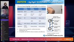
Stretchable silicone-based medical devices with AgCl fillers?
In general, silicone based conductive pastes are rare and the versions with AgCl fillers- needed for many medical wearable applications- are even rarer! David Dewey from FUJIKURA KASEI Co Ltd unveiled this paste for the first time in June at TechBlick. The pastes can offer 1-10 E-4 ohm/sqr when cured at 150C for 30min or so on substrates such as PET or silicone sheet. These inks are compatible with other silicone-based (insulator, adhesive, etc) out of Fujikura's portfolio, enabling one to print complex multi-layer medical wearable devices on stretchable substrates like silicone! To learn more visit www.TechBlick.com or join the industry in Eindhoven on 12-13 OCT 2022 https://www.techblick.com/electronicsreshaped #silicone #stretchable #wearable #skinpatch #printedelectronics...

15 August 2022
Conformal EMI shielding based on particle-free inks
Conformal EMI shielding is a megatrend on its way to become ubiquitous in electronics. The incumbent process is based on sputtering a tri-layer structure consisting of SUS (stainless steel)- Cu-SUS (total stack is 3-6um typically) on the EMC (epoxy molding compound) of the package. Hikaru Uno from Merck & Melbs LeMieux from Electroninks Incorporated show an alternative based on non-vacuum spray coating of particle-free Ag inks. In these slides, you can see performance analysis and detailed cost analysis/projections. The incumbent (sputtering) is a well established technique with many market reference from the likes of Apple and Samsung. However, it is a vacuum process requiring substantial CapEx investments with a large production footprint. The sputtering deposition rate will also be low given the required film quality. Sputtering is poor at side wall and deep trench coverage, resulting in large thickness variations between the top and side walls. Spraying the EMI shielding can address some issues: it is a non vacuum process with a low Capex and a high unit-per-hour (UPH) throughput and is able to offer uniform side and top wall coverage. The spraying can be used with Ag or Cu nanoparticles. Both nanoparticle techniques though suffer from expensive materials, potential for nozzle clogging and thus production downtime, and even relatively thick required coatings. To overcome these shortcomings, particle-free silver inks can be sprayed. Is this technique effective? The bel...
15 August 2022
Innovation in a Pandemic
Speaker: Stan Farnsworth | Company: NovaCentrix| Date: 10-11 March 2021 | Full Presentation Even with the challenges of the past year, innovation has moved forward. Stan will take a look at how a few of the key tech trends have fared in the past year, such as 5G, AI, and IoT. He will also connect those to the printed and flexible electronics space, and why we should pay attention to those universal trends. Finally, he will touch on his own experiences with innovation at NovaCentrix, and consider aspects of sustaining innovation versus true disruption. Join TechBlick on an annual pass to join all live online conference or online version of onsite conference access library of on-demand talks (600 talks + PDFs) portfolio of expert led masterclass year-round platform https://www.techblick.com/ And do NOT miss our flagship event in Berlin on 17-18 OCT 2023 focused on Reshaping the Future of Electronics. This event attracts 550-600 participants from all the world and offers a superb ambience and dynamic exhibition floor. To learn more visit https://www.techblick.com/electronicsreshaped To see feedback about previous event see https://www.techblick.com/events-agenda...