



11 July 2022
R2R-NIL for realizing highly innovative use cases – from bionics to medical diagnostics
This is an auto-generated transcript to help the video. It has not been proof read by a person threfore they may be errors
So, yeah, thank you very much. And for the opportunity to give a talk here and show the introduction of what we are doing in the field of roll to roll UV nano printing, lithography. So Joanneum Rresearch located in Austria we have one vision with this process from nano goes macro. So I don't know if all of you are familiar with UV nano imprint. And so we have the ability to produce very small structures on large scale, so on large and mechanically flexible substrates. And the first step we have to apply a coating resin. Then the next step is the molding. So the giving, the coating, the structures and the subsequent curing via UV and then the molding. And finally you have the structure. So it seems to be quite a simple process for a highly complex and very small structures. And what we have established over the last decade that Joanneum Research is so called patterning pilot line where we start with the material. So we develop our own material, which is a anneal cure. It's like polyurethane or acrylics, which we can adjust to the specific needs a little bit later on. Then we have the simulation and the design by software tools to identify the optimal structure. Then we make the mastering. So with, for example, mala, so maskless laser lithography and the upscaling from the master by step and repeat to really have a full shim equipped with those structur...
11 July 2022
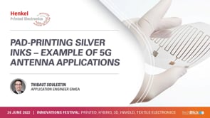
Pad printing silver inks- example of 5G antenna applications
This is an auto-generated transcript. It has not been proof read by a person threfore they may be errors This is your Thibaut. It's a pleasure for me to talk about the new range of product that we have developed by printing silver ink. So Henkel is well known for the sale of conductive inks, especially for screen printing. But we have a nice project in China where one of our customers ask for printable inks for antennas, and basically we develop those inks, especially to meet the customer demand, but also because it really answers to product requirements, especially it combines two trends. The main trend that we see is the trend of connectivity. We have all heard for many years about Internet of Things, you know, is the 5G. We are even talking about the Internet of everything in that the objects we have to communicate together. We have also to communicate to people, but also to cloud in order to process the data, in order to enable seamless communications between everyone and everything you need high quality antennas and they. Other trend that we will see also is the one of 3D electronics, because we want to have smaller and smaller objects with even higher integral functionality also always customized. So basically you want to turn some maybe thermoplastic enclosure into smarter ones. And the best way to to make it is maybe to incoperate components on plastic surfaces or to bring or so connectivity. So we have developed by printing for those who are not familiar with pad p...
11 July 2022
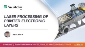
Laser processing of printed electronic layers
This is an auto-generated transcript to help the video. It has not been proof read by a person threfore they may be error
All right, perfect. The stage is yours. Thank you. So had everyone as already told. My name is Jonas Martin from Fraunhofer Ilt in Germany. And I'm going to present you some of the work related to printed electronics now. So as a first small hint, what are we doing? Who are we? I'm coming from the group fields of film, film processing, a form of ilt, and we're covering in detail five different topics, all about things and processing. So the first one is about cleaning, painting, pretreatment of layers or substrates. The second one is about corrosion, corrosion resistance and anti stick layers. The third one is about energy and mobility means a particular battery technology and hydrogen technology. And the two topics I'm going to detail today are printed electronics and embedded sensors and microelectronics in particular, also by printing technology. So our approach to what's printed electronics, we are using laser radiation sources for the additive production of electronic layers. Depending on this, we typically have about four process steps, not too different from those you already know from printed electronics. So firstly, we usually do a surface pre-treatment mainly via laser radiation, but we do also use sometimes more conventional techniques like plasma treatment and so on. Secondly, we do the position of the layers, mainly with lasers, also by indu...

11 July 2022
Digital Printing: Microdispensing, Electrohydrodynamic Printing, LIFT, Selective-Area Jet Metallizat
Digital fineline printing is one of the most important developments in additive electronics. Inkjet itself has come very far with excellent progress even towards R2R industrialization. However, inkjet has two limitations as a technology: (1) limited resolution, (2) limited ink viscosity range, and (3) limited throughput per print head. Here, we highly several digital and hybrid technologies that can overcome these limits. XTPL- microdispensing with innovative non-Newtonian highly-loaded NP pastes The first is the microdispensing technology developed by XTPL with nozzle diameters in the range of 0.5-12um. It demonstrates a unique combination of ultrafine line (few micron) 'digital' printing on flat and non-flat surfaces AND highly conducting (40% Ag bulk?) highly viscous nanoparticle (Ag, Cu, Au) pastes. Thus, this technology advances the art not just by extenting the resolution of digital printing beyond what inkjet achieves but also by enabling far more conductive and highly loaded conductive pastes. The innovation here is not just the microdispensing machine, but also the unique non-Newotonian highly-loaded nanoparticle pastes. The AgNP pastes have high loading (>85 wt% in some cases), small particles (45nm), and are in ethylene glycol solvents. The pastes require relatively high sintering temperatures (250-300C) but offer high conductivity, e.g., 4.2 uOhm.cm for the ink with 80wt% loading. In the first slide below you can learn about the microdispensing machine itself. It ...

11 July 2022
DuPont MCM | Demonstration of high-frequency 5G modules using LTCC
Brian J. Laughlin, Ph.D. Lead Scientist, Brian.j.laughlin@dupont.com Visit our web portal: https://www.dupont.com/brands/microcircuit-and-component-materials.html While the infrastructure, devices, and applications of 5G telecommunications are evolving, the need for circuits which operate at the higher frequency millimeter wave (mmWave) bands is clear. High-frequency circuit operation presents many challenges, including the need to create efficient RF signal processing and wireless transmission which can generally be achieved via increased integration that allows shorter communication paths. Also, advanced materials that enable both heterogenous integration of disparate active devices (e.g., Si, GaAs, GaN, and SiC) and passive devices (e.g., SMD, antennae, filters, etc.) while providing stable operation and low losses in a variety of environments are critical performance considerations. DuPont™ GreenTape™ Low-Temperature Co-fired Ceramic (LTCC) tape and silver (Ag) metallization delivers excellent high-frequency performance in designs optimized for high reliability and long life—even in the most challenging environments. Figure 1: GreenTape™ dielectric constant (Dk) and dielectric loss (Df) measured by a Fabry Perot from 20 to 100 GHz. As part of an initiative to demonstrate the high performance of GreenTape™ and create a reference design that goes beyond a basic material datasheet, DuPont Microcircuit and Component Materials (MCM) partnered with Dr. Chun-An “Ivan” Lu at the ...
11 July 2022
Critical to performance metrics of functional materials for IME
This is an auto-generated transcript to help the video. It has not been proof read by a person threfore they may be error Okay. Excellent. Thank you, everyone. Good to be here. Thanks for an opportunity to speak here. My topic is critical to performance metrics of functional materials for IMC, so I'm going to try to cover some of the highlights and key points in this 5 minutes that I have here. For those that are not familiar with Sun Chemical, we are the largest ink coating and pigment supplier. I work personally in the division for Advanced Materials. We offer materials for electronics. You can see different applications here on this slide, but I will be really focusing on our suntronic materials for printed electronics and more specifically on in mold electronics. So we the topic is the requirements or requirements metrics, performance metrics for IAM. So as you can imagine, inmold electronics includes multiple process steps and it comes from printing label printing which is typically screen printing. Then it goes to say SMT assembly, it goes to 3D forming injection molding. So it's a quite, quite interesting process. But then it's not only the materials need to meet, not only performance related to process such as print ability process, stability, stability on, on, on press drying and things like that, but also 3D forming, which is really, you know, you're stretching a conductor. You you're making the cross section smaller, you're thinning the conductor, you're narrowing...
11 July 2022
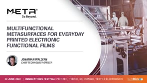
Multifunctional Metasurfaces for everyday printed electronic functional films
This is an auto-generated transcript to help the video. It has not been proof read by a person threfore they may be error Thank you. Well, good morning, everybody. I represent metamaterials and we're developing discrete platform specific proprietary technologies for large area lithography, similar to the previous speaker in a sense. But I guess where we differentiate is that to a certain extent we have a roll to rolll manufacturing of these films. So the large area allowing the manufacture of these nanostructures to be carried out in a very cost effective manner. So each platform that we have employs massively parallel patterning scheme designed to be scalable in these large areas of either rigid substrate materials or rolls of flexible film. And in certain cases we use phase shift masks approach to actually pattern them. And in others we use a new type of class cast plasmonic printing, all allowing for the creation of structures with feature sizes down to about 50 nanometers. Metamaterials are complex structures, as we just learned and patterned into conventional materials such as metals or plastics, in ways that perform special functions, such as transparently blocking a specific level of light, for instance, in one of our products for anti reflective glasses to prevent people from laser strikes, etc., or performing multiple optical functions in, say, a lens which we're also working on. So what I'd like to do today is just zero in or just one of our platforms, nano web in ...
11 July 2022
Stretchable Electronic Materials that Meet the Demands
This is an auto-generated transcript to help the video. It has not been proof read by a person threfore they may be error Hello, everyone. I'm Andrew Baumbach. And I'm the Stretchable electronics product manager at ACI Materials. I'll do a brief overview of our our stretch portfolio and I'll start with talking a little bit about the patented cavitation processing tool that we use here to manufacture these inks. And basically what we're doing is we're harnessing the power of cavitation, which you can think of as exploding microbubbles. And it allows us to achieve levels of dispersion that conventional mixing cannot achieve. And this is all done without damaging functional fillers, which can be a problem with with some mixing technology out there. And it's a very highly controlled process and it's all automated. And this helps give excellent batch to batch consistency. And this is especially true when you're talking about carbon based materials to the particles high aspect ratio, things like carbon nanotubes, graphene, things like that that are extremely difficult to disperse. And now going into the stretch product portfolio, I'll talk about the 11 and nine. This is our silver conductor. You can think of this as the interconnects and the bus bars that are used in wearable electronics. We'll go over some of the performance data on the next slide. The SC 5025, that's the fixed resistance, stretchable heatsink. And so this is used for printing wearable heaters that heat very unif...