


5 February 2025
Photovoltaic Technology: Record Module Efficiencies, Scalable STOPVs, Mass-Customizable Solar Solutions and Next-Gen Manufacturing
This newsletter points out the interesting improvements in solar power technology. Dr. Stéphane Cros of CEA presented improvements from the Apolo European project and these improvements included record module efficiencies near 19% and understandings into laser scribing, deposition uniformity and encapsulation issues. Dr. Emma Spooner, at the University of Manchester, intensely studies scalable semi-transparent organic photovoltaics (STOPVs) for windows and building-integrated PV. She collaborates with Contra Vision to develop remarkably revolutionary OPV stacks. Lena Reinke of Panacol presents several highly effective adhesive solutions and these solutions considerably improve the durability and electrical reliability of a large number of flexible solar modules. Francesca Scuratti of Ribes Tech uses advanced roll-to-roll (R2R) additive manufacturing and organic photovoltaics to overcome several IoT2 challenges and enable energy independence. Aldo Kingma of Solliance presented meaningful progress. This progress involved developing a pilot line for several cost-effective and flexible PV laminates, easing their smooth integration into buildings and infrastructure. CEA | Apolo story for the manufacturing of record modules (11 cm2) close to 19% efficiency University of Manchester | Scalable Semi-transparent Organic Photovoltaics Panacol | Adhesive Solutions for Perovskite-based and Organic Photovoltaic Applications Ribes Tech | Fully printed additive manufacturing for indoor pho...
23 January 2025
Additive electronics and future of spacecrafts and deployed structured?
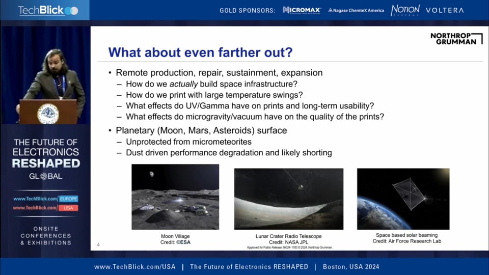
Additive electronics and future of spacecrafts and deployed structured? Watch this video of the talk from Anthony DeCicco how printed sensors are crucial, saving technician time/effort, and how ink technology is becoming reliable and high quality enough for these long lifetime (15+++ year) applications..... Join us at TechBlick USA show on 11&12 June to learn how additive electronics will enable in-space manufacturing. Explore the program here https://lnkd.in/gQKjBZzn 🌌 Monitoring Deployed Space Structures Monitoring the performance of large, deployed space structures over time is a significant challenge, requiring numerous strain sensors across the structure. Solution: Printing sensors directly onto structures could drastically reduce technician time and streamline production. 🖋️ Advancements in Ink Technology Tremendous progress in ink technology and reliability, thanks to efforts by academia and industry consortiums like NextFlex. Focus is shifting toward print quality and long-term reliability for advanced applications. 🚀 Durability for Space Missions Spacecraft components must endure lifetimes of 15+ years, with some geosatellites already surpassing 25 years. Degradation impacts performance, thermal management, and spacecraft operations—making reliability critical. ⚡ Approaching Bulk Conductivity Recent advancements in reactive ink printing have achieved ~85% bulk conductivity, marking a significant step forward. The next challenge: Understanding the effects of lo...
22 January 2025
The need for R2R and HIGH SPEED printing of perovskite solar photovoltaics?
Thomas Tombs at Energy Materials Corporation explained why at TechBlick 's Future of Electronics RESHAPED show in Boston last here, outlining that the demand will be 75 terawatts of need by the year 2025! Join us on 11 and 12 June again in Boston to RESHAPEE the FUTURE of ELECTRONCIS making it additive, printed R2R, flexible etc. Explore the program --> https://lnkd.in/gQKjBZzn Stephan DeLuca #Perovskites #PrintedElectronics #R2R #Additive #TechBlick #ElectronicsRESHAPED...

20 January 2025
Voltera: Dispensing Solder Paste on Factory Fabricated PCBs
Printed circuit boards (PCBs) are essential for electronic circuits, providing mechanical support and electrical connections for components. Factory fabricated (or sometimes called prefabricated) PCBs are pre-manufactured, ready-to-use boards that simplify assembly and ensure consistent quality in electronic devices. Contact: sales@voltera.io or +1 888-381-3332 ext: 1 Summary of Materials and Tools MATERIALS USED T4 Solder Paste Sn42Bi57.6Ag0.4 SUBSTRATES USED Factory fabricated PCB (FR4) TOOLS AND ACCESSORIES V-One PCB printer Tweezers Clamps Thumb screws Disposable nozzles Project Overview Purpose The purpose of this project was to demonstrate the feasibility of dispensing solder paste on factory fabricated PCBs precisely and reflowing the solder paste automatically. Design The board we selected for this project was a PCB used in the module hub of our NOVA material dispensing system . Since we designed the board in-house, we had the Gerber file for this project, which we uploaded into V-One’s software. Gerber file loaded into the V-One software Desired outcome The solder paste should be evenly dispensed on the designated spots of the FR4 board, with no overflow or voids. Once reflowed, the PCB should fit into the bottom of NOVA’s module hub. When connected to power, this board will allow NOVA to capture images of its work area. Front view of NOVA showing its module hub and work area Functionality The PCB contains a camera, LEDs, and other components that enable NOVA to c...

4 February 2025
Indium Bump Interconnect (IBI) Flip Chip Bonding | finetech GmbH
Abstract – The increasing demand for technologies such as infrared (IR) thermal imaging sensors, quantum processors, and micro-LED displays drives the need for advanced interconnect solutions. These technologies require fine-pitch Indium Bump Interconnects (IBI) for high-density flip-chip bonding. Larger chip sizes, sub-micron alignment, and extreme environmental conditions pose significant challenges. This paper highlights solutions addressing these challenges, enabling high-quality bonding for IR thermal sensors and other applications. I. Introduction Indium Bump Interconnect (IBI) is crucial for applications like IR thermal sensors, quantum processors, X-ray detectors, and micro-LED displays. Among these, IR sensors represent a demanding use case, requiring precise bonding of fine-pitch micro Indium bumps to substrates. Challenges include maintaining co-planarity, preventing contamination, and ensuring mechanical and electrical reliability. II. Indium Bump Interconnect Flip Chip Die Bonding Die bonding process Bonding methods range from cold compression to thermal compression and formic acid reflow, depending on application requirements. Achieving high yield during trials and production is critical due to the high cost and complexity of materials. Material preparation and handling Indium bumps are vacuum-deposited and protected with photoresist. Cleaning and kitting processes minimize contamination and handling risks, reducing preparation time and ensuring material integr...
23 January 2025
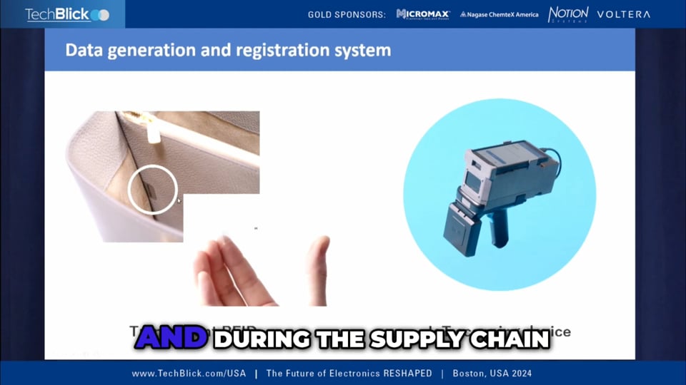
R2R printed ultrafine transparent RFID for supply chain management
阿部誠之 from Asahi Kasei explains how their R2R printed ultrafine transparent RFID will be part of a total system including blockchain to enable brand owners to achieve full supply chain management Join us in Boston on 11 and 12 June to learn what more about applications of additive and printed electronics across all sectors. Explore the upcoming program now https://www.techblick.com/electronicsreshapedusa...

21 January 2025
Flexible Circuits, E-Textiles, and Wearable Electronics: SSAIL, Graphene Fibers, and Embroidery Technology
This edition dives into the cutting-edge innovations shaping the future of flexible circuits, e-textiles, and wearable electronics. Discover how industry leaders are leveraging technologies like SSAIL, embroidery, graphene fibers, and advanced inks to redefine scalability, durability, and performance across applications. From health monitoring wearables to thermal-regulating textiles, we highlight breakthrough solutions driving adoption in industries such as healthcare, aged care, and fitness. Key topics include SSAIL’s rapid circuit development, Celanese’s stretchable inks, Kyorene® fibers' antibacterial benefits, and embroidery’s automated precision in creating functional textiles. Stay informed on the challenges, advancements, and real-world applications of these transformative technologies. Akoneer | Using SSAIL technology for fast development of flexible circuits RMIT University | Stretchable and flexible electronics reshaped for industry-driven aged-care technologies Celanese | Time to Think Beyond Stretch in Wearable Electronics Graphene One | Graphene based functional fibers for clothing and textiles 3E Smart Solutions | Driving Reliability and Scalability in E-Textiles and Wearables via Embroidery Technology The Future of Electronics RESHAPED USA is TechBlick's premier event, showcasing the latest innovations in electronics. Join us at UMass Boston on June 11-12, 2025 for an exciting exploration of emerging technologies. You can find more details on the event ...

17 January 2025
R&D Funding Opportunities, Flexible Printed Electronics, Advanced Battery Technologies, and IoT Applications
TechBlick wishes you a wonderful 2025! In this edition, we highlight, NETO Innovation specializes in securing funding for R&D projects through programs like Horizon Europe, EIC, and Eureka, with expertise in green energy, printed electronics, healthcare, and advanced materials. Yamagata University showcases advancements in flexible, printed carbon-based sensors for IoT applications, focusing on high-sensitivity pressure, strain, and humidity sensors for robotics and healthcare. Ensurge leads in anode-less solid-state lithium microbattery technology, offering superior energy density, rapid charging, and ultrathin packaging to address scale-up challenges for IoT and wearable devices. Kimoto presents cutting-edge adhesive and protective film solutions for precision manufacturing, including residue-free adhesives, high-transparency coatings, ESD protection, and advanced converting techniques like die-cutting and laser cutting. As we enter 2025, we’re excited to continue sharing the latest insights, trends, and opportunities in emerging technologies. Thank you for your continued support we look forward to connecting with you in our upcoming events. NETO Innovation | Unlock your project's full potential with NETO Innovation Yamagata University | Flexible Printed Carbon-based Sensors and Their Applications Ensurge | Manufacturing Scale-Up of mAh Class Anode-less Solid-State Lithium Microbatteries Kimoto | Adhesive Carrier and Protection Films for Advanced Manufacturing Join us o...