


Fine-Pitch Direct Die Attach Without Thermal Compression | SunRay Scientific
- Oct 26, 2023
- 6 min read
Andrew Stemmerman & John Yundt SunRay Scientific Inc. Eatontown, NJ USA
andrew@sunrayscientific.com johny@sunrayscientific.com
SunRay Scientific of Eatontown, NJ, USA has developed a new and innovative approach to electronic component assembly.
This article will outline the developments of this technology and show examples of this magnetically aligned Anisotropic Conductive Epoxy packaging method used on various substrates. Progress will be shared for dense and fine pitch Land Grid Arrays (LGA) on a semi-rigid interposer.
Introduction
Flip-chip die and die-to-die bonding, from dense to fine pitch, typically require solder balls and underfills. Underfill and/or edge encapsulant is often utilized to provide additional mechanical strength and stress reduction. The result is a complex assembly process flow. Localized placement of Anisotropic Conductive Adhesive (ACA) or Anisotropic Conductive Film (ACF) for specific components typically involves the fine-pitchuse of thermocompression bonding, an additional process step that could also be damaging to thin silicon. Another drawback for traditional interconnect materials is relatively slow processes, limiting the utility of such technologies. Development towards a wafer scale compatible packaging method will be shared, using a pressure-less and low-temperature magnetically aligned Anisotropic Conductive Epoxy (ACE).

Figure 1. Flip Chip assembly comparisons: traditional solder balls & underfill attachment (Left); Die attach with z-axis magnetically aligned conductive epoxy (Right)
A summary of the novel approach is shown above in Figure 1. First, ferro-magnetic particles dispersed within an epoxy are coated onto a substrate. The ferro-magnetic particles form z-axis magnetically aligned columns, fixed in place during the die-to-substrate cure process without any pressure applied. The formation of the columns during the curing process is illustrated in Figure 2. This technology simplifies the assembly process to a single adhesive application, which provides both electrical interconnection and mechanical reinforcement. No additional underfill material is needed. Fine patterning is not required as the entire area of the component target location is deposited with epoxy. The device alignment process is more
forgiving relative to solder ball-to-solder pad alignment. Z-axis columns align after component placement, magnetic pallet exposure and cure is achieved.

Figure 2. X-Ray photos of Z-axis magnetically aligned particles ferromagnetic in an Anisotropic Conductive Epoxy (ACE)
Thermal or UV curing methods complete the component attachment without any thermocompression (cure method is epoxy formulation dependent). Thermal curing occurs within the 80°C to 160°C temperature range.
This article outlines the developments of this technology and shows examples of this magnetically aligned Anisotropic Conductive Epoxy packaging method used on various substrates. Progress will be shared for dense and fine-pitch Land Grid Arrays (LGA) on a semi-rigid interposer. Additionally, advancements made for die-to-die bonding will be presented as well as updates towards achieving ≤ 60-micron pitch. Other proposed direct die-attach packaging concepts will be illustrated.
Example #2 covers development work performed on attaching a 126-pin Land Grid Array (LGA) bare die to a polymer semi-rigid multi-layer substrate. The use of the substrate resulted in multiple challenges for bare die attach. The non-planarity of the conductive circuit pads was one issue. The electrical resistance variation between pads had to be minimized for optimum performance. The non-uniformity of the substrate’s conductor pads is evident in the photo on the left. The schematic on the right illustrates how the ACE material allows for “leveling” in connecting the bare die to the non-planar substrate.
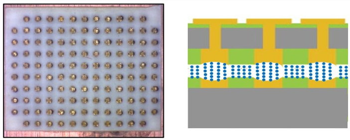
Figure 3. 126-pad semi-rigid substrate (Left) and illustration of bond between die and substrate
Additional learning during this work was in identifying trapped moisture within the polymer-based substrate as a cause for voids in the ACE during cure. These bubbles not only prevented connection in some cases but interfered with proper z-axis column formation. Prebake for the substrate was added as a step for this particular type of assembly.
Two formulations were the focus of the work in Example #3. These were the Fine particles ACE and the Ultra Fine particles version. Stencil thicknesses of 0.001” to 0.005” were studied, as this tool has the most impact on establishing bond line thickness. The target for choosing the best formulation, tool and bond line thickness was lowest average resistance values with lowest deviation among the 126 pads. Iterative testing was done. “Heat maps” based on the 126 pad locations were created to visually observe resistance values within set target and acceptance ranges. The next two Figures show results from early work on process development with each epoxy formulation and stencil tools, to the progress made with the final choices on material and stencil thickness. Ultimately the Ultra Fine particles ACE with a 0.001” thick stencil was chosen for this LGA-to-substrate assembly application. Summary Table 1 shows the results of the chosen ACE and stencil, and Figure 6 is a cross-section from the development study.

Figure 4. Pad-by-pad resistance measurement studies, early iteration (Left: Ultrafine, Right: Fine)

Figure 5. Pad-by-pad resistance measurement studies, final iteration (Left: Ultrafine, Right: Fine)
Table 1. Summary of performance metrics (continuity, resistance & deviation, pad-to-pad)
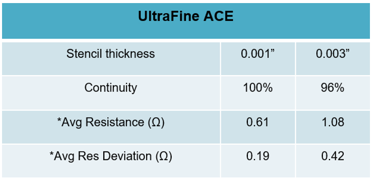

Figure 6. Cross-section of component attached and electrically connected with the Z-axis ACE (Photo courtesy of Rochester Institute of Technology)
Example #2 takes the LGA and Substrate subassembly to the next level, a large area 8” x 10” circuit board populated with four of the subassemblies plus components of various sizes and function. This larger assembly involves attaching all the multiple components and subassemblies in one ACE attachment process. Passives range in size from as small as 0201 up to 2220. Other devices are a 26-pin SMT connector and SoICs. This project is underway, and results will be shown by SunRay at TechBlick live in October.
Fine-pitch die-to-die bonding with the ACE is the third example. The development methodology is like the other projects. An initial focus was on measuring continuity and resistance at pad sites as part of identifying the optimum process parameters and stencil tool for this application. The degree of difficulty is greater with finer pitch. Dense arrays of 60 microns pitch die, with 30 microns pads and 30 microns spacing, were used.

A Design of Experiments (DoE) was established for the stencil studies. Laser profilometry was used for 3D and 2D scans of the two surfaces to be bonded, as was employed for observing the non-planarity of the semi-rigid board in Example #1. All initial steps were done manually: hand stencil printing, die placement with die bonder, batch oven cure and electrical probing.
Prior to using fully functional devices, Quartz substrates patterned with the top layer of each die in the bond pair, were procured and used in early studies. The purpose was to provide enhanced analysis of the bonded die pair before, during, and after bonding/curing has occurred. Bond parameters were observed at each step of the process: pre-bond, bond, and post alignment & cure.
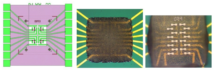
Figure 7. Left: Target overlay of quartz substrates; Middle: ACE deposit before bond; Right: Post-bond, before z-axis alignment and cure
Due to the finer pitch requirements, the test vehicles have a nickel layer applied during wafer fabrication, at the bond pad locations. Past experimentation, as pictured in Figure 8, has shown nickel application may lower the resistance of the bonded circuit by directing column formation to the metallized bond pad boundary, the nickel pads, acting as localized magnets, attract column formation during exposure to the magnetic pallet. This only applies to the bond pads themselves, to concentrate the ferromagneticmetalized particles within the ACE more towards the connection points. This creates a higher density of columns within each pad.

Figure 8. Left: No nickel interlayer and ACE; Right: ACE after cure with Nickel interlayer layer in pads
Conclusion
Besides the addition of the nickel layer to the functional die, key parameter targets were updated for the project’s next phase. In the short-term alignment, fiducials on the quartz plates were updated to improve bonding in X, Y, and theta; and the size of test probe pads were increased to improve accuracy and reduce testing time.
The development efforts for all three examples are still underway. The conclusions thus far are:
Successful demonstrations of Heterogenous Packaging using z-axis magnetically aligned epoxy for structural & electrical bonding.
Similar established process techniques and test methodologies are usable across applications, although each has unique requirements.
The Ultra Fine particles ACE formulation has the best performance for finer pitches and more challenging alignments.
Uniform bond lines between device pads are critical for optimum electrical performance.
Excellent performance results were obtained, even with manual assembly techniques. Performance will improve with automation.
In concept this z-axis magnetically aligned conductive epoxy approach could integrate multiple silicon wafers on top of each other, creating the possibility for an exceptionally dense integrated System-In-a-Package (SIP). Processing temperatures can be as low as 80°C, opening room for alternate substrates and biocompatible assemblies. This anisotropic epoxy is not limited to specific device attachment; it can be used to bond multiple component sizes and styles across an entire substrate.
Comments