


The Depth & Breadth Of Innovation In The Display Industry (I)
- Jun 28, 2021
- 12 min read
Updated: Sep 17, 2021
TechBlick Highlights
We are publishing a series of two articles this week, highlighting the depth and breadth of innovation in the display industry. This article includes more than 40 individual images and charts showcasing various innovations in microLED, microOLEDs, quantum dots, printed displays, phosphors, TFTs, AI in displays, reflective displays, nanoimprinting, AR/VR and beyond. You can see the table of content for this article below.
In this article:
Behind-display imaging and AI to shape the future of video conferencing
Laser-induced forward transfer & photonic soldering for large-area microLED displays
Xerographic-based digitally-controlled micro-assembly for microLED & microchip transfer
Enabling GaN LED epitaxial growth on large-area substrates (vs wafers)
Towards Mask-Free RGB high-PPI directly-patterned microOLEDs
Printing in tiling and transfer/placement of mini- and micro-LEDs
Setting benchmarks for evaluating the reliability of flexible/rollable displays
All the innovations highlighted in these articles are from companies presenting or exhibiting at our upcoming LIVE (online event) on Innovations & Market Trends in Displays. This event will take place in nearly two weeks, on 14-16 July 2021.
Add the event dates to your Calendar: Google Calendar | Microsoft Outlook Calendar | Office 365 Calendar | Yahoo Calendar
With a single Annual Pass, you can participate in all our LIVE events online, truly mingle and network with the community online, and participate in our masterclasses. See how our networking and virtual mingling work here
With the Annual Pass, you can also access an ever-growing Netflix-like library of up-to-date presentations on emerging technologies (currently 160 presentations).
You can see the full agenda here. You can buy your annual pass for just 450 Euros per year using the 10% discount code 10%DiscountAA until 7 June 2021.
Speakers Include

And many more...
Betting on the right display technology for the future
After the demise of plasma, LCD has been dominating the TV market for more than a decade. OLED was once thought to be a sure winner for the next generation of large display technologies. After all, it delivers infinite contrast, perfect blacks, vibrant colors and proponents have long been promised that cost will ultimately match or even beat that of LCD. But OLED have failed to deliver on that latter promise.
In the meantime, LCD cost keeps coming down while performance and size trend up: Quantum Dots are already widespread in high end LCD TVs and now propagating into mid-range models. MiniLED backlights are used by most TV makers in their 2021 flagship models. New technologies are emerging. The first QD-OLED panels should be available later in 2021. In the longer term, microLED, nanorod LEDs, and QLEDs are all promising alternatives for TV applications.
But OLED are not standing still. Better materials such as TADF or phosphorescent blue could improve performance in term of brightness and color, Inkjet Printing could finally help deliver on the cost promise. This profusion of new technologies is exciting for the consumer.
For display makers it represents both an opportunity and a strategic headache: developing advanced display technology and setting the fabs cost billions of dollars. How can they ensure that they’re betting on the right technology?
At TechBlick, Yole will present its view of the technology trends in the display industry particularly in the mid or large sized segmentt. The schematic below is a snapshot of these trends. In the OLED field, we have gone from bottom to top emission white OLED. We are now transitioning towards QD-OLED.
To learn more join TechBlick’s upcoming LIVE(online) interactive conference on Displays & Lighting: Innovations & Market Trends (14-16 July 2021) with an Annual Pass

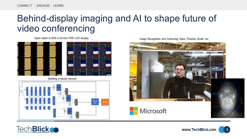
Behind-display imaging and AI to shape future of video conferencing
These days we spend our days in front of computers, engaged in video call after video call. Often, the camera is not well positioned, giving an awkward and unnatural feel to the conversation. In fact, a common complaint is that conversation do not feel natural and one misses body language clues. This will change in time.
A major trend is to image through the screen (vs. camera on the top edge). This will give a much better and natural view. The challenge, of course, is that transmission through the display is low. For LCDs, the open aspect ratio is around 53%. Furthermore, at IR, the transmission is much higher than visible. Indeed, many suppliers are development display sheets that are IR transparent now. This will allow one to place a LED laser source and an IR-sensitive camera behind the screen.
The advances in machine vision will play an incredibly important role in displays. Neutral networks are being developed to offer face recognitions and later gaze, blur, scale and position correction to make the conversation as natural as possible.
This is an extremely hot trend in the field of displays, both in terms of algorithm development and development displays that are IR transparent. Every player in the field is involved. At TechBlick, you will hear from one of the leading research teams in the field, Microsoft, developing the cutting-edge in the area.
To learn more join TechBlick’s upcoming LIVE(online) interactive conference on Displays & Lighting: Innovations & Market Trends (14-16 July 2021) with an Annual Pass.
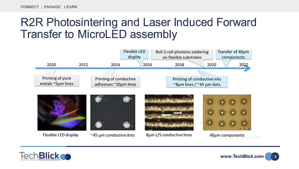
Laser-induced forward transfer and photonic soldering for large-area microLED displays
Holst is at the forefront of innovation in printed, flexible, and large-area electronics. They often set the tempo and direction of research. In this case, they have been working on many technologies which, when brought together, can enable large-area rapid microLED assembly.
The R2R photonic soldering on flexible substrate is an excellent method that can accelerate soldering (attachment) of microLEDs onto the substrate. When optimised, it can take place on the scale of milli seconds (compared it with timescales of classic reflow for solder or heat curing for ECAs).
LIFT or Laser Induced Forward Transfer offers a way to transfer the microLEDs onto the substrate at speed. Here, pulses from an ultraviolet (excimer) laser enter through the backside of the carrier, which is transparent. The laser light is absorbed in the thin layer of adhesive which has been holding the µLEDs to the temporary carrier and vaporizes it. This physically blows the µLEDs off and pushes them onto the final display panel, which is placed in close contact. Adhesive on the final glass panel holds the µLEDs in place. This method allows LEDs made on sapphire to be transferred economically over large areas at high speed.
To learn more join TechBlick’s upcoming LIVE(online) interactive conference on Displays & Lighting: Innovations & Market Trends (14-16 July 2021) with an Annual Pass
Cartridge-based printing in microLED transfer
One of the main challenges in microLED fabrication is a high-yield (>>99.999%) and high-throughput transfer process. Many approaches have been developed. Some interesting techniques involve some form of printing (stamp transfer, R2R, etc). Here, I only highlight two interesting approaches.
The first is from VueReal who is developing a cartridge-based approach. The process is shown below. Here, the donor substrate containing the microchips is brought into contact with the receiver substrate. The two substrates are then aligned before the transfer takes place. There is a need to apply some force mechanism to overcome the force keeping the microchips attached to the donor substrates. This force is likely to be a combination of thermal and mechanical.
VueReal partners have access to end-to-end production ready tools, high yield verified microLED and cartridge process (99.999%), and a commercially available microprinter tool for 30x40 cm2 substrate using VueReal technology.
To learn more join TechBlick’s upcoming LIVE(online) interactive conference on Displays & Lighting: Innovations & Market Trends (14-16 July 2021) with an Annual Pass.

Xerographic-based digitally-controlled micro assembly for microLED and microchip transfer
Another interesting, earlier stage, development is by Parc, a Xerox company. The idea is based upon xerographic printing. Here, microchips such as micro GaN LEDs are suspended in a solution. They are then cast onto an active-matrix substrate controlling a 2D array of electrodes which generate electrostatic force to spatially move the individual chips under the gaze of a camera.
The 2021 demonstrator is still small size (2.5 x 2.5 cm) on 50um LEDs with no yield data. The assembly process is achieved using a projector addressing a photoswitch array. The assembly process, from mass disordered deposition from liquid to final alignment, is shown below. Currently it is too slow, but an order of magnitude improvement can make it competitive.
The process has interesting development potential as it does not require any special microchip structure. The alignment and positioning is also software controlled, thus allowing arbitrary and complex shapes.
To learn more join TechBlick’s upcoming LIVE(online) interactive conference on Displays & Lighting: Innovations & Market Trends (14-16 July 2021) with an Annual Pass

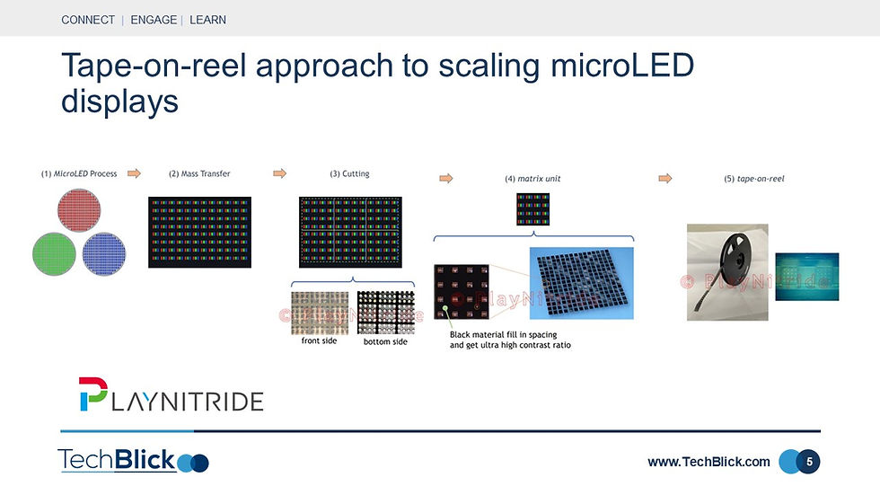
Tape-on-reel approach to scaling microLED displays
There are many incredible innovations in the microLED field. Another one that we wish to highlight is in creating a method to assemble large-area microLED displays from tape-on-reel approach.
This is shown below. Here, the microLEDs are first transferred into a larger panel and are then cut into smaller tiles. The tiles undergo an inspection step and the black filling material is added to enhance contrast. The titles are then added onto a reel, creating a tape-on-reel approach enabling the construction of large microLED displays using a SMT-like process! This is a very interesting innovation in the field by PlayNitride.
To learn more join TechBlick’s upcoming LIVE(online) interactive conference on Displays & Lighting: Innovations & Market Trends (14-16 July 2021) with an Annual Pass
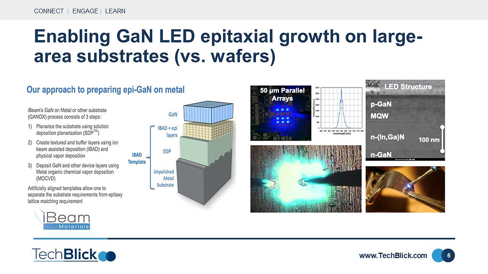
Enabling GaN LED epitaxial growth on large-area substrates (vs. wafers)
Epitaxy is today carried out on rigid single-crystal wafers to make GaN LEDs. This yields high-quality low-defect LED wafers but over limited areas. But what if LEDs could be grown on large-area substrates such as glass or metal foils?
iBeam Materials is developing a new technology for large-area LED epitaxy. By using a thin metal foil substrate iBeam can make the single-crystal templates for LEDs in a roll-to-roll (R2R) process. The key to the process is an ion-beam crystal aligned layer that sits between the metal foil and the epitaxial layer of GaN. This allows for making epitaxial GaN sheets in very large areas and potentially at very low cost, enabling large-area monolithic integration of optical and transistor devices.
This technology is very interesting, albeit still at a low-tech readiness level. It has a tiny, almost negligible, fraction of the accumulated experience that wafer-based LED industry has. It is in fact yet to fully assess QY, lifetime, economics and other important factors of GaN LED growth on large-area substrate. Nonetheless, it is a promising approach.
To learn more join TechBlick’s upcoming LIVE(online) interactive conference on Displays & Lighting: Innovations & Market Trends (14-16 July 2021) with an Annual Pass.
Towards Mask-Free RGB high-PPI directly-patterned microOLEDs
The need for bright high-PPI microdisplays is clear, particularly in AR/VR glasses. MicroOLED are a mature technology option, especially when it comes to the white OLED plus color filter technology.
The table below benchmarks various options. The white OLED/color filter approach has high PPI but limited brightness (color filters waste 1/3 of power). The direct RGB OLED can have higher brightness but currently the PPI is now as high.
Imec is developing an interesting RGB OLED technology based on direct photolithography of OLED. In previous years, it had demonstrated single color displays. It is now outlining a route towards RGB high-PPI displays.
As driver circuit, Imec is using BEOL technology to realize IGZO TFTs allowing 3.6µm RGB-ready pixels, corresponding to 7055ppi. In parallel, it is developing a special fabrication line and a single process flow to develop photolith-patterned RGB microOLEDs. The proposed process is shown below.
This is still a work in progress as many challenges are to be overcome, particularly around degradation minimization during etching, plasma exposure, chamber exchange, thermal and UV steps, etc. Nonetheless, Imec will show results at TechBlick showing no observable degradation in the OLED lifetime with and without patterning (T95@1000 nits >200h).
To learn more join TechBlick’s upcoming LIVE(online) interactive conference on Displays & Lighting: Innovations & Market Trends (14-16 July 2021) with an Annual Pass.

High PPI directly patterned (via mask) microOLED
eMagin is the technology leader in high-PPI high-brightness RGB microOLED. Over the years they have been making excellent progress. They have gone from 20k cd/sqm in 2011 to some 7000 cd/sqm in 2021 with the short-term target and mid-term (2023) targets being 10000 cd/sqm and 28000 Cd/sqm, respectively. In terms of resolution, they have progressed from VGA (640x480) to now 2kx2k (2049x2048). Note that 7k Cd/sqm was for RGB WUXGA resolution. This product has well established military and aviation customers.
The technology is based on evaporated RGB OLED via a very fine mask. The mask is created by etching through a PECVD SiNx coated silicon substrate. As such, the fine RGB patterns are achieved via direct patterning and evaporation (no photolithography).
This is a relatively mature technology with an established customer base in military and aviation but with a still significant room for improvement. The products are currently all US based (see clean room below).
To learn more join TechBlick’s upcoming LIVE(online) interactive conference on Displays & Lighting: Innovations & Market Trends (14-16 July 2021) with an Annual Pass.

Printing in tiling and transfer/placement of mini- and micro-LEDs
Aerosol Jet technology enables panel front to backside connections without glass vias or vacuum processes. Aerosol jet can print high resolutions, down to 10 μm, and at a high aspect ratio, as high as 5mm from the substrate regardless of topology. It can print 36,000 and 18,000 interconnects per hour in the to-edge and full-wrap cases, respectively (both 0.5mm long).
At TechBlick, you will hear about a demonstration of high-speed, high-density printing of connections from the front side of a panel to the backside along with examples of repair of existing metallization created by other methods.
Screen printing can also be used in micro-LED displays. It can be used in via filling or in depositing the bonding material for the mini- or micro-LEDs, e.g., ECAs or solder paste. Furthermore, screen printing can be used to print the connection lines between the mini- or micro-LEDs and the outside circuit. Finally, screen printing can also print the wrap-around electrodes. In this case, the substrate will be precisely rotated as the printing takes place. This approach too will eliminate the need for vacuum processes.
This diversity of applications means that screen printing can have its place, for example, in via filling, even when vacuum PVD processes are utilized.
The image below is from Applied Materials showing that edge electrodes with L/S of 30µm/50µm can be printed (the actual shown example is with L/S of 40µm/60µm).
To learn more join TechBlick’s upcoming LIVE(online) interactive conference on Displays & Lighting: Innovations & Market Trends (14-16 July 2021) with an Annual Pass.

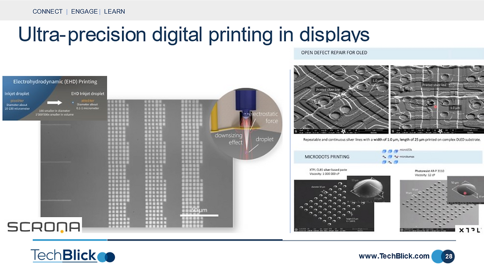
Ultra-precision printing in display repairs
Electrohydrodynamic jet (EHJ) printing brings the resolution of digital functional printing to the 0.1-1 µm range, as shown below. In many cases, the EHJ printers are single nozzle, limiting their industrial applications as throughout remains constrained. Scrona is developing a system with 12 print heads.
The image below (left) shows printing of quadratic patches using Scrona’s printhead. Those patches of material are printed with silver inks, but can also be printed with other inks, e.g., quantum dot inks. One interesting application can be in deposition of colour conversion filters on microLEDs.
What is important to note in the image below is that one can see 12 identical regions which were printed by 12 nozzles on Scrona’s printhead. The multiple nozzles essentially replicate the output and increase throughput, laying the foundation of an industry high-throughput ultra-precision system.
XTPL is also developing ultra-precision digital printer able to print very fine features on flat and non-flat surfaces using their special micro-dispensing machines and highly viscous Ag nanoparticle ink system.
There can be interesting applications in the display industry too. In the image below (right, bottom), you can see that this print head is applied to print Ag nanoparticle based micro bumps. In another example (right, top), the system is being applied to repair open defects in an OLED displays
To learn more join TechBlick’s upcoming LIVE(online) interactive conference on Displays & Lighting: Innovations & Market Trends (14-16 July 2021) with an Annual Pass.
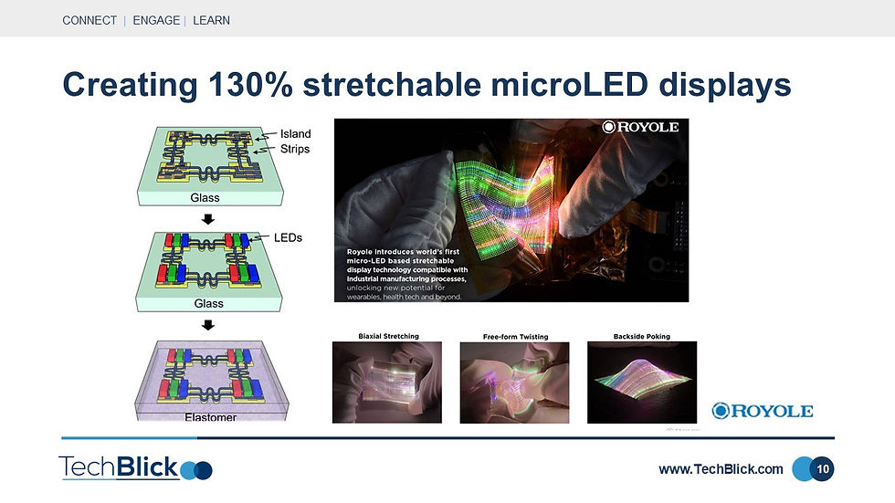
Creating 130% stretchable microLED displays for healthcare
There has often been talk and tech demonstrators of stretchable displays, mainly focusing on OLEDs. However, Royole, the first to commercially launch a fully flexible display worldwide, has demonstrated a stretchable microLED display. The advantage here is that microLEDs can have smaller aperture sizes and do not require encapsulation like OLEDs.
To achieve stretchability, the classic island-plus-wavy interconnect approach is utilized. Here, a small aperture translates into a smaller rigid islands, improving stretchability.
The production process flow is shown here. The device is manufactured on a flexible substrate put on a temporary glass substrate. The micrLEDs are transferred and bonded using microLED assembly methods such as pick-and-place, printing, etc. The entire circuit is then delaminated off the temporary glass and encapsulated by an elastomeric material like silicone, TPE, or rubber.
Royole demonstrated a 2.7 inch stretchable and transparent display containing 90x150µm LEDs in a 0.6mm pixel pitch (42 PPI), showing stretchability up to 130%.
To learn more join TechBlick’s upcoming LIVE(online) interactive conference on Displays & Lighting: Innovations & Market Trends (14-16 July 2021) with an Annual Pass.
Setting benchmarks for evaluating reliability of flexible/rollable displays
The chart below shows the trend towards large displays. At the same time, it also shows the transitions in mobile phone display technology: LCD to Glass OLED to Plastic OLED and now to foldable/rollable displays.
Reliability of these foldable/flexible displays is still not as mature as conventional (rigid) devices. For example, as shown here, when incorporating thin cover window film/glass for curved and foldable devices, new failure modes (crease, delamination, buckling, scratches, low energy impact, …) will become important. New reliability tests will need to be defined to correctly assess the performance of these devices.
At TechBlick’s upcoming conference, Google will be outlining the latest test methodologies for mechanical, environmental and surface durability assessment of foldable displays

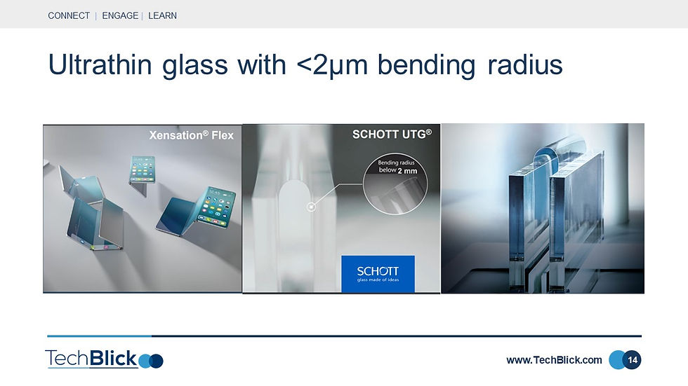
Ultrathin glass with <2µm bending radius
Flexible and foldable glass already has a long history of development. I recall the first time I saw the Corning flexible display when I was still at student some 12-13 years ago. The technology has come a long way since.
In particular, various approaches have been developed to improve bending and hinder crack formation and propagation. Schott is one of the leaders in the field with a track record of success in commercialising its flexible glass as a cover glass in mobile phones.
At TechBlick, Schott will present its latest progress. As shown below, Schott can now achieve <2mm bending radius.
Comments