Search Results
1063 results found with an empty search
- The future of additive manufacturing – EHD printing technology redefines boundaries
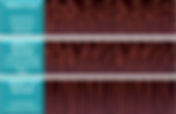
The status quo of additive manufacturing and inkjet printing How EHD technology is pushing the boundaries EHD in practice – applications for industry Implementation of EHD technology into the Notion Systems ecosystem The status quo of additive manufacturing and inkjet printing Author: Simon Rihm | Notion Systems |https://www.linkedin.com/in/rihmsimon/ (1) The status quo of additive manufacturing and inkjet printing Over the past two decades, additive manufacturing has undergone a profound transformation, evolving from a technology primarily confined to prototyping into a cornerstone of modern industrial production. This transformation is driven by its high flexibility, strong potential for customization, shorter development cycles, and efficient use of materials. By depositing material only where needed, additive processes significantly reduce waste compared to conventional methods - an advantage that is particularly important for expensive or scarce materials such as titanium alloys or high-purity metals. Additionally, additive manufacturing enables the production of complex structures that are difficult or impossible to achieve with traditional techniques, leading to lighter and higher-performance components. The growing significance of additive manufacturing is especially evident in the electronics and semiconductor industries. These fields are defined by ongoing miniaturization, increasing integration density, and extremely stringent precision requirements. Conventional lithographic and mechanical fabrication methods are progressively approaching their technological limits, particularly in the context of flexible substrates, novel material systems, and cost-efficient large-area production. In this regard, additive technologies, most notably inkjet printing, offer decisive advantages and are becoming increasingly integrated into production processes worldwide. From both an economic and technological perspective, it is becoming increasingly untenable to disregard the trend toward additive manufacturing. In most cases, the required investment amortizes rapidly, further reinforcing its attractiveness. It is therefore only a matter of time before additive manufacturing establishes itself as a dominant paradigm in industrial production. (2) How EHD technology is pushing the boundaries While inkjet printing is a well-established digital manufacturing technique, its inherent limitations - particularly in terms of feature size, ink viscosity, and adaptability to complex surfaces - restrict its use in advanced microscale research and semiconductor-grade applications. Electrohydrodynamic (EHD) printing addresses these challenges by utilizing electrically driven jetting mechanisms. This approach enables the fabrication of structures in the single-digit micron range, supports a much wider range of ink viscosities, and operates entirely contactlessly. As a result, EHD printing allows precise patterning on non-planar and sensitive substrates, opening new possibilities in areas such as semiconductor packaging, heterogeneous integration, advanced interconnects, sensor technologies, and emerging nanoelectronic devices. The key to these advantages lies in the fundamentally different droplet generation mechanism. In conventional inkjet systems, droplets are formed by pressure waves generated via piezoelectric actuation, which forces ink through a nozzle and inherently limits droplet size to the nozzle diameter while incurring energy losses due to fluid resistance. In contrast, EHD printing generates droplets through electric fields acting directly on the conductive liquid. This creates a balance between electrostatic forces and surface tension, forming a meniscus at the nozzle tip where energy is highly concentrated. Droplets are emitted from this localized region, allowing feature sizes significantly smaller than the nozzle diameter. Image 1: Comparison of droplet formation This alternative droplet generation mechanism offers several significant advantages. By decoupling droplet size from nozzle geometry, EHD printing substantially expands both the range of processable ink viscosities and the achievable resolution. While conventional inkjet systems typically produce feature sizes between 30 µm and 50 µm, EHD printing can achieve resolutions below 5 µm. At the same time, the viscosity window is greatly extended: whereas inkjet printing is generally limited to around 30 cP, EHD systems can handle viscosities exceeding 10,000 cP. However, such extreme conditions often require specialized printhead designs and may involve trade-offs in resolution, making it necessary to carefully balance viscosity and precision depending on the application. Beyond droplet formation, the controlled transport of droplets is crucial for high-quality results. In EHD printing, electric fields are used not only to generate droplets but also to guide them with high precision. Unlike conventional methods that deposit material on predefined planar positions, EHD dynamically adapts to the substrate’s topography. This enables accurate patterning on curved, stepped, or otherwise irregular surfaces, significantly broadening the range of compatible geometries and allowing the fabrication of three-dimensional electronic structures and advanced packaging solutions. Overall, this represents a substantial technological advancement over traditional inkjet processes, opening up new possibilities for manufacturing and functional integration. (3) EHD in practice – applications for the industry In practical applications, EHD printing is increasingly emerging as a key enabling technology across a wide range of disciplines. Its unique capability to combine ultra-high resolution, broad material compatibility, and precise, contactless deposition fundamentally expands the design space available to engineers and researchers. Unlike conventional manufacturing approaches, EHD does not merely optimize existing processes - it enables entirely new ones. This shift is particularly relevant in fields where established fabrication technologies are approaching physical, economic, or material-related limits. Against this backdrop, EHD printing acts as a technological catalyst, unlocking new degrees of freedom in device architecture, material integration, and system performance. The following application areas are intended to illustrate where the strengths of EHD technology lie. a. Enhanced topography printing Topography printing enables precise material deposition on complex, non-flat surfaces and represents a key advantage of EHD-based processes. In particular, the MEMS-based printheads developed by Scrona ensure highly accurate and consistent droplet placement, even on curved, stepped, or irregular structures. This capability significantly surpasses conventional printing methods and opens new opportunities for the realization of three-dimensional electronics and advanced packaging solutions. Closely related to this is the concept of step printing, which allows controlled material deposition across discontinuities such as edges, gaps, or height variations on a substrate. This is particularly critical for applications in advanced packaging, conformal coatings, and optical structures. By enabling high-resolution, distortion-free printing over complex three-dimensional features, EHD technology avoids issues such as material overflow and loss of precision. As a result, it unlocks new degrees of design freedom and facilitates the development of increasingly sophisticated and integrated device architectures. Image 2: Printing on topography with commercially available conductive silver ink b. Novel display technologies The rapid evolution of display technologies - driven by applications such as augmented reality (AR), virtual reality (VR), and next-generation consumer electronics - is placing unprecedented demands on resolution, brightness, and energy efficiency. Emerging concepts such as Micro-LED and Quantum Dot displays are widely regarded as key candidates to meet these requirements. However, their large-scale and cost-efficient manufacturing remains a significant challenge. In this context EHD printing systems provide a fundamentally new approach to display fabrication. One of the central challenges in Micro-LED displays lies in the precise placement and patterning of color-converting materials, such as quantum dots, at extremely small pixel pitches. Conventional techniques - often relying on photolithography or transfer printing - face limitations in scalability, alignment accuracy, and material efficiency. EHD printing overcomes these barriers by enabling the direct, maskless deposition of quantum dot materials with sub-micron precision and highly controlled layer thickness. This capability allows for the fabrication of high-brightness, full-color microLED displays, where pixel density and optical performance are critical. Beyond microLEDs, EHD technology also offers significant advantages for established display technologies such as OLED and LCD. By simplifying layer deposition processes and reducing reliance on complex masking steps, EHD can streamline manufacturing workflows, lower production costs, and enable more flexible design iterations. c. Advanced semiconductor packaging As the scaling of transistors in accordance with Moore's Law approaches both physical and economic limits, the semiconductor industry is undergoing a paradigm shift. Increasingly, performance gains are being achieved not through further miniaturization of individual transistors, but through innovations in system integration and packaging - an approach commonly referred to as “More than Moore”. Advanced packaging techniques - such as heterogeneous integration, chiplet architectures, and 3D stacking - require new methods for interconnection, material deposition, and fine-structure fabrication. Traditional photolithographic processes, while highly precise, are often cost-intensive and inflexible when applied to these emerging architectures, particularly for non-planar or heterogeneous substrates. EHD printing introduces a transformative alternative by enabling high-resolution, additive structuring directly onto wafers, chips, or package substrates. Its capabilities extend across a wide range of applications, including wafer and chip marking, solder bumping, via filling, and the direct patterning of redistribution layers (RDLs). The latter is especially significant, as RDLs are critical for routing electrical signals in advanced packages. With its ability to achieve micrometer resolution and high aspect ratio structures, EHD printing is uniquely suited for fabricating dense interconnect architectures required in next-generation devices. Moreover, the digital, maskless nature of the process offers the potential to reduce fabrication costs by up to an order of magnitude compared to conventional photolithography, while simultaneously increasing design flexibility. d. High-definition structures Antenna printing represents another important application of EHD-based additive manufacturing, enabling the precise deposition of conductive materials to form high-performance antenna structures. This is particularly relevant for devices such as consumer electronics, drones, and IoT components, where compact design and reliable signal transmission are essential. Image 3: Ultra-fine, low-loss antenna structures on various substrates EHD technology allows the fabrication of ultra-fine, low-loss antenna patterns on a wide range of substrates, significantly improving signal quality while supporting ongoing miniaturization. At the same time, it facilitates seamless integration of antennas into increasingly compact and complex electronic systems. As a result, EHD printing contributes to the development of highly efficient, space-saving communication components and expands the design possibilities for next-generation electronic devices. Image 4: Conductive silver traces, 3 µm line width (4) Implementation of EHD technology into the Notion Systems ecosystem Through an exclusive collaboration, Notion Systems and Scrona have successfully translated advanced electrohydrodynamic printing into a user-friendly, high-precision research platform: the n.jet EHD. This partnership combines Notion Systems’ expertise in functional material printing systems with Scrona’s innovative multi-nozzle MEMS-based EHD printhead technology, aiming to accelerate the adoption of EHD printing in fields such as display technology, electronics manufacturing, and semiconductor production. Within this framework, Notion Systems is responsible for manufacturing and servicing the n.jet EHD, which is specifically designed for advanced research and development applications. The system offers ultra-high precision and stability, including a printing resolution below 5 µm, repeat accuracy down to 1 µm, and a motion system with seven independently controlled axes. Additional features include an encoder resolution of 10 nm and support for substrates up to 150 × 150 mm. Mechanical stability is ensured through a granite base and vibration isolation, while integrated high-resolution top and bottom microscope systems enable precise alignment and real-time process monitoring. As with conventional inkjet technologies, printheads play a decisive role in determining overall process performance. In the case of the n.jet EHD system, the latest generation of multi-nozzle MEMS printheads developed by Scrona (Gen3) significantly expands the operational capabilities available to the user. These printheads enable not only extremely high-resolution patterning but also the reliable processing of inks with elevated viscosities. Whereas traditional inkjet systems typically reach their functional limits at viscosities above approximately 50 cP, Scrona’s Gen3 printheads can handle viscosities of up to 300 cP while maintaining high print quality. The advanced capabilities of the latest generation of EHD printheads are further reflected in a range of highly optimized technical features that enhance both process stability and application flexibility. Building on the multi-nozzle MEMS architecture, these systems are designed to meet the stringent requirements of high-resolution, high-performance additive manufacturing in research and industrial contexts. Image 5: GEN3-128 (128 nozzles) and GEN3-8 (8 nozzles) printheads The current generation of printheads is available starting from configurations with eight nozzles (Gen3-8), enabling parallelized material deposition and thereby increasing throughput without compromising precision. A key innovation lies in the implementation of nozzle-level ink circulation, which ensures consistent ink delivery, minimizes the risk of clogging, and contributes to overall process reliability - particularly when working with functional materials of higher viscosity. Thermal management is another critical aspect: integrated printhead heating of up to 75 °C allows precise control over ink rheology during operation. This capability is essential for stabilizing jetting behavior and expanding the range of compatible material systems. Image 6: Printed EHD sample We are exhibiting at The Future of Electronics RESHAPED in California, USA on 10-11 June 2026 Please register to meet us in person and see our technology in action. Join the flagship TechBlick events in California on 10-11 June 2026 This event is the global hub for Additive, Printed, Sustainable, Hybrid and 3D Electronics. It is where the global industry connects, where the latest is unveiled and where big products, novel ideas and key projects and partnerships are discussed and forged. This event is not to be missed!
- Introducing the Electronics RESHAPED USA Program - Material Innovations in Printed Electronics
The Future of Electronics RESHAPED USA conference and exhibition ( 10 & 11 JUNE 2026, Mountain View ) is set to be the most important event of the year in Silicon Valley focused on additive, hybrid, 3D, sustainable, wearable, soft and textile electronics. Hosted at the iconic Computer History Museum , this event serves as the global hub for the next generation of electronics. This year the program features a world-class agenda with over 75 superb invited talks from around the world, 8 industry- or expert-led masterclasses , 2 tours , and over 75 onsite exhibitors . In this article, we discuss and highlight various innovative talks at the event around the theme of Material Innovations in Printed Electronics . In previous articles we covered process advancements, R2R manufacturing, smart surfaces and sensing, printed photovoltaics and more. Explore the full agenda now and join the global industry in Mountain View on 10 & 11 JUNE 2026 . Let us RESHAPE the Future of Electronics together, making it Additive, Hybrid, 3D, R2R, Soft, Flexible, Wearable, Textile and Sustainable. 🚨 Explore the Full Agenda and Register before 3 May when early bird rates expire Tatsuta – Robert Wilson discusses silver-coated copper particle conductive pastes . Robert explores the critical challenge of copper oxidation, which severely impacts the reliability of low-cost interconnects when replacing expensive silver. By engineering silver-coated copper particles, Tatsuta combines the cost advantages of copper with the stability of silver. This work offers a scalable, eco-friendly solution for PCB and FPC manufacturing, reducing CO₂ emissions to 18% compared to traditional subtractive etching. Copprint – Ofer Shochet discusses the structural shift from silver to copper inks . Ofer explores how the surge in demand from EVs and data centers has created a "Silver Tax," imposing a $24B+ burden that directly compresses margins for printed electronics manufacturers. The presentation maps the transition landscape, highlighting how high-performance copper inks now offer a viable substitute for silver. This solution provides an intelligent risk-management framework for manufacturers to reclaim margins through direct material substitution. Electroninks – Mitchell Smith explores Silver MOD Inks as an advancement beyond particle pastes . Mitchell explores the chemical limitations of traditional particle-based pastes, which often require high-temperature curing and high metal loading. Metal-organic decomposition (MOD) inks achieve comparable conductivity using less metal and can be cured at much lower temperatures. This work offers a pathway for integrating high-performance electronics onto heat-sensitive plastic substrates that were previously incompatible with standard conductive pastes. 🚨 Explore the Full Agenda and Register before 3 May when early bird rates expire 👉 iGii (Integrated Graphene) – Michelle Ntola highlights 3D carbon nanomaterials (Gii) . Michelle explores the volatile pricing and supply chain risks associated with metal-heavy electrode formulations in microheaters and batteries. Gii is a proprietary 3D carbon platform that delivers robust thermal performance (up to 400 °C) and high surface quality without relying on silver. This technology offers a sustainable, drop-in alternative for roll-to-roll manufacturing, capable of producing up to 80 million parts per year. 👉 Arieca Inc. – Navid Kazem discusses liquid metal embedded elastomer (LMEE) composites for AI cooling. Navid explores the thermal bottleneck in next-generation high-performance computing, where power densities are projected to reach 4 W/mm², far exceeding the capabilities of current thermal interface materials (TIMs). LMEEs combine the high thermal conductivity of dispersed liquid metal microdroplets with the mechanical compliance of soft elastomers. This work offers a transformative TIM solution that reduces data center power consumption by effectively managing heat in large silicon dies with significant warpage. Graphene Engineering Innovation Centre – Andrew Strudwick presents printed electronics based on graphene and 2D materials . Andrew explores the "tipping point" of graphene, moving from lab curiosity to real-world solutions for environmental monitoring and health sensors. The talk highlights how GEIC's pilot-scale printing equipment helps companies bridge the gap between material research and product launch. This solution offers partners a world-class facility to design, develop, and scale the next generation of energy-efficient heating elements and flexible devices. 🚨 Explore the Full Agenda and Register before 3 May when early bird rates expire Nagase ChemteX – Brandon Peters discusses innovations in fine line conductive ink printing . Alan explores the complex interplay between ink chemistry, screen parameters, and substrate surface energy that often prevents reliable sub-micron printing features. The presentation examines how optimizing mesh count and emulsion profiles can improve line definition and electrical performance. This work offers a practical roadmap for manufacturers to achieve consistent, ultra-fine resolution across diverse advanced electronic applications. Henkel – Julie Ferrigno explores materials and processes for printed antennas . Julie explores how high-frequency designs require low surface roughness and uniform thickness, which are difficult to achieve with standard silver pastes. The talk presents silver-filled and emerging silver-plated copper (SPC) inks that deliver comparable RF behavior at lower costs. This solution enables high-throughput manufacturing of 3D antenna structures via pad printing, facilitating the mass adoption of smart connectivity. Heraeus Electronics highlights optimizing design principles for PTC heater circuits . The talk explores the common manufacturing challenges with printed carbon-based heaters, such as print consistency and resistance tolerance under accelerated processing. In collaboration with Boyd, Heraeus investigates how print formfactor and roll-to-roll conditions impact heat-up characteristics. This work offers a set of best practices to enhance both the performance and manufacturability of flexible heaters for automotive and personal devices. 🚨 Explore the Full Agenda and Register before 3 May when early bird rates expire University of Southern California – Hangbo Zhao explores high-resolution liquid metal-based stretchable electronics . Hangbo explores the difficulty of achieving feature sizes below the standard limit for liquid metal patterns used in implantable biomedical devices. By integrating colloidal self-assembly and micro-transfer printing, patterns as small as 5 µm are realized. This work offers a method for creating cardiac mapping devices that maintain exceptional conductivity (2.4×10⁶ S/m) even under extreme 1200% strain. Sunray Scientific – John Yundt discusses fine-pitch direct die attach with reduced cost and higher throughput . John explores the constraints of traditional bonding technologies like solder and silver-filled ECAs, which often suffer from brittle properties, low bond strength, or slow micro-dot dispensing. ZTACH® ACE utilizes magnetically aligned columns of ferromagnetic particles to create an anisotropic electrical interconnection. This work offers a pressure-less, low-temperature process that simplifies assembly to a single step while increasing bond strength by 5-10x. ACI Materials – Richard Morris highlights materials for durable FHE and E-Textiles . Richard explores the issue of galvanic corrosion in electrically conductive adhesives (ECA) under damp heat, which limits the durability of wearables. The presentation introduces solderable printed conductors that enable higher-density circuits and smaller SMDs. This solution provides a cost-effective, additive pathway for manufacturing stretchable e-textiles that can withstand harsh environmental conditions. Applied Nanotech Inc. – Richard Fink concludes with novel ink development for extreme environments . Richard explores the lack of functional inks capable of maintaining electrical integrity under the extreme temperatures and pressures found in aerospace and industrial monitoring. The presentation details the characterization and testing of specialized conductive formulations. This work offers a robust material set designed to ensure reliability where conventional printed electronics would fail. 🚨 Explore the Full Agenda and Register before 3 May when early bird rates expire
- Introducing the Electronics RESHAPED USA Program - Wearable Sensors, Actuators and Soft Robotics
The Future of Electronics RESHAPED USA conference and exhibition ( 10 & 11 JUNE 2026, Mountain View ) is set to be the most important event of the year in Silicon Valley focused on additive, hybrid, 3D, sustainable, wearable, soft and textile electronics. Hosted at the iconic Computer History Museum , this event serves as the global hub for the next generation of electronics. This year the program features a world-class agenda with over 75 superb invited talks from around the world, 8 industry- or expert-led masterclasses , 2 tours , and over 75 onsite exhibitors . In this article, we discuss and highlight various innovative talks at the event around the theme of Wearable Sensors, Actuators and Soft Robotics . In other articles we cover themes like materials innovation, additive electronics in packaging and PCBs, wearables and sensors, soft robotics, additive electronics in packaging and PCB production, sustainable electronics, and more. Explore the full agenda now and join the global industry in Mountain View on 10 & 11 JUNE 2026 . Let us RESHAPE the Future of Electronics together, making it Additive, Hybrid, 3D, R2R, Soft, Flexible, Wearable, Textile and Sustainable. 🚨 Explore the Full Agenda and Register before 3 May when early bird rates expire GE Healthcare – Gurvinder Singh Khinda discusses sustainability in single-use medical sensors and devices . Gurvinder explores the significant environmental burden of biohazardous single-use products and the sanitation issues inherent in the biomedical industry. The talk highlights the use of Flexible Hybrid Electronics (FHE) and environmentally conscious design practices to create sustainable demonstrators like vital sign monitors. This work offers a life cycle assessment (LCA) methodology to reduce costs and environmental impact in medical device manufacturing. Medtronic – Dr. Rohan Sonawane discusses Data and AI in Cardiac Monitoring . Rohan explores the challenge of "data overload," where care teams are overwhelmed by vast streams of information that lack timely, meaningful insight. The session focuses on AI algorithms that interpret continuous physiologic data to filter out false signals and identify early signs of risk. This solution shifts healthcare from reactive responses to proactive prevention, improving both clinical efficiency and the patient experience. Genentech (Roche Group) – Paul Upham explores wearables in pharma . Paul explores the need for objective, real-world data from a patient's environment to develop more accurate clinical endpoints during drug development. The presentation provides use cases for how wearable technology can measure disease progression and treatment efficacy across multiple domains. This work offers pharmaceutical researchers a critical tool for improving the accuracy and impact of clinical trials. 🚨 Explore the Full Agenda and Register before 3 May when early bird rates expire 👉 Stanford University – Angela McIntyre highlights wearables as embodied AI . Angela explores the shifting paradigm where wearable devices are no longer just passive sensors but are becoming active participants in human-AI interaction. This talk examines how integrating intelligence directly into the wearable form factor enables more intuitive and responsive user experiences. This technology offers a glimpse into a future where "embodied AI" seamlessly supports health, productivity, and physical interaction. 👉 GE Aerospace – Deepak Trivedi highlights FHE-enabled soft robotics . Deepak explores the opportunities and challenges of moving away from rigid robotic systems toward flexible, soft-bodied machines that can safely interact with humans and complex environments. The talk examines how Flexible Hybrid Electronics (FHE) act as the "nervous system" for these robots. This work offers a technical roadmap for overcoming integration hurdles to realize the full potential of soft robotic systems. 👉 Artimus Robotics – Eric Acome discusses the development of polymer-based electrohydraulic actuators . Eric explores the limitations of traditional electric motors, which are mechanically complex, generate high heat, and are difficult to miniaturize for next-gen robotics. By combining thin polymer films and liquid dielectrics, Artimus has developed "HASEL" actuators that function like artificial muscles. This solution offers a high power-to-weight ratio and fast response times for dexterous robotic hands and wearable devices. 🚨 Explore the Full Agenda and Register before 3 May when early bird rates expire NGK Insulators LTD – Masahiro Furukawa introduces ceramic-based Li-ion rechargeable batteries for health monitoring . Masahiro explores the safety and form-factor constraints of organic-based batteries in close-contact wearable patches for preventive care. These ceramic-based batteries feature a semi-solid structure that is thin, bendable, and exceptionally safe for skin contact. This technology offers a multi-year storage solution with fast-charging capabilities, optimized for home disease management devices. Quad Industries – Wim Christiaens discusses scaling wearable printed electronics for mass-market applications . Wim explores the technical gap between promising lab prototypes and the reliable, repeatable manufacturing required for large-scale commercial success. The presentation uses case studies to show how design choices and process development influence final production costs. This work offers an industrial perspective on moving wearable systems from the laboratory to cost-effective mass production. Screentec – Antti Tauriainen discusses the future of supply chains for medical electrodes . Antti explores how shifting medical regulations and environmental requirements are creating instability in traditional material supply chains. The session covers approaches to design that account for technical, usability, and environmental requirements for disposable goods. This solution offers new strategies for manufacturing and supply chain management to ensure a steady supply of high-quality medical sensors. 🚨 Explore the Full Agenda and Register before 3 May when early bird rates expire University of North Carolina – Wubin Bai explores a multi-modal noninvasive in vivo biosensing system . Wubin explores the limitations of existing muscle tracking devices, which often rely on indirect surface measurements or specialized skin adhesion. This system utilizes near-infrared (NIR) light to capture muscular locomotion while an IMU decouples complex motion signals. This AI-boosted solution offers an adaptive model for classifying muscle activities, facilitating better diagnostics for neuromuscular disorders. University of Southern California – Hangbo Zhao presents high-resolution liquid metal-based stretchable electronics . Hangbo explores the difficulty of achieving scalable, high-resolution patterning for liquid metal circuits used in cardiac mapping and soft robotics. By integrating colloidal self-assembly and micro-transfer printing, feature sizes as small as 5 µm are achieved. This work offers a method for creating microelectrode arrays that maintain high performance even under 1200% strain. Yamagata University – Shizuo Tokito highlights flexible printed sensors for robotic hands . Shizuo explores the lack of human-like tactile sensing in current robotics, which prevents machines from handling fragile objects with precision. The talk details the use of porous piezoresistive layers and piezoelectric polymer inks printed on flexible substrates to emulate human skin. This work offers a lightweight, conformable sensing system that allows robotic hands to detect pressure, texture, and temperature. 🚨 Explore the Full Agenda and Register before 3 May when early bird rates expire Datwyler Switzerland Inc. – Mattia Lucchini discusses unlocking internal physiological and mental insights via next-gen wearables . Mattia explores how current wearables focus almost exclusively on external behavior and activity levels, missing deeper contextual health data. The session reviews advancements in functional materials that enable the continuous collection of EEG and EMG biosignals. This solution offers a transformative opportunity for objective assessments of a user's mental and physiological status through sensor fusion. Texavie – Peyman Servati explores MarsWear smart apparel for personalized therapy . Peyman explores the discomfort and lack of accuracy in traditional wearable devices used for long-term health monitoring and clinical assessment. MarsWear integrates yarn sensor technologies and machine learning into comfortable apparel to provide real-time feedback with high fidelity. This platform technology offers a groundbreaking solution for personalized wellness, gaming, and AR/VR control. VTT – Tuomas Happonen highlights elastic multilayer printed circuits (EMPC) . Tuomas explores the challenges of manufacturing sensitive, interference-tolerant elastic circuits using traditional rigid PCB methods. The approach uses stacked, pre-perforated TPU films with screen-printed filled vias to create robust multilayer architectures. This work offers an industrially feasible sheet-based process for creating complex, flexible circuits suitable for wearable RF applications. Voltera – Giovanni Obando and East West Manufacturing conclude with mass-producing wearable biosensors . The sessions explore the specific challenges of printing silver conductive inks directly onto cotton fabrics and scaling these biosensors for volume production. By validating optimal print settings for textiles, these works move the industry closer to truly integrated "smart clothing." These combined solutions offer a pathway to mass-producing reliable, fabric-based heaters and biosensors for consumer and medical markets. 🚨 Explore the Full Agenda and Register before 3 May when early bird rates expire
- Introducing the Electronics RESHAPED USA Program - Hybrid Electronic Manufacturing and Scale-Up
The Future of Electronics RESHAPED USA conference and exhibition ( 10 & 11 JUNE 2026, Mountain View ) is set to be the most important event of the year in Silicon Valley focused on additive, hybrid, 3D, sustainable, wearable, soft and textile electronics. Hosted at the iconic Computer History Museum , this event serves as the global hub for the next generation of electronics. This year the program features a world-class agenda with over 75 superb invited talks from around the world, 8 industry- or expert-led masterclasses , 2 tours , and over 75 onsite exhibitors . In this article, we discuss and highlight various innovative talks at the event around the theme of Hybrid Electronic Manufacturing and Scale-Up . In other articles we cover themes like materials innovation, additive electronics in packaging and PCBs, wearables and sensors, soft robotics, additive and 3D electronics, sustainable electronics, and more. Explore the full agenda now and join the global industry in Mountain View on 10 & 11 JUNE 2026 . Let us RESHAPE the Future of Electronics together, making it Additive, Hybrid, 3D, R2R, Soft, Flexible, Wearable, Textile and Sustainable. 🚨 Explore the Full Agenda and Register before 3 May when early bird rates expire NextFlex – Dan Gamota discusses manufacturing readiness for hybrid electronics . In this session, Dan explores the lack of standardized data and validated qualification pathways that currently slow the transition from lab innovation to industrial deployment. Emphasis is placed on roadmapping technical needs for defense and commercial sectors, including high-reliability interconnects. This work offers improved validation frameworks to accelerate the commercialization of complex integrated systems. Smooth & Sharp Corporation – Alan Wu presents a proven R2R production solution for NFC antennas . Alan explores the complexity barriers that usually prevent additive manufacturing from moving beyond single-layer UHF antennas to sophisticated electronic functions. The talk reveals successful large-scale mass production techniques for multi-layer RFID/NFC circuits. This work offers proof that complicated circuit designs are now possible at scale using additive R2R processes. TracXon – Ashok Sridhar unveils high-density printed electronics with VIAs . Ashok explores the fundamental limitation where a lack of printed vertical interconnects (VIAs) prevents printed electronics from reaching the complexity levels of traditional etched PCBs. TracXon is building the first dedicated VIA filling machine compatible with R2R lines to enable double-sided circuitry. This solution provides the missing link for high-density printed electronics, significantly closing the gap with traditional manufacturing. 🚨 Explore the Full Agenda and Register before 3 May when early bird rates expire 👉 Intellivation LLC – Mark George highlights an R2R platform for active and passive thin films . In this talk, Mark explores how the high cost of mask fabrication and labor-intensive lithography steps hinder rapid product development for flexible sensors. By combining sputtering with in-line laser ablation, multi-layers can be patterned without damaging sensitive substrates. This technology offers a high-throughput, mask-less manufacturing method for fully functional semiconducting devices. 👉 Quad Industries – Wim Christiaens discusses scaling wearable printed electronics for the mass market . Wim explores the "valley of death" where promising laboratory prototypes fail to meet the reliability and repeatability standards required for industrial manufacturing. The talk uses case studies to analyze how material selection and design choices directly impact cost-effective production. This session offers a roadmap for translating functional wearable prototypes into reliable, mass-market products. Henkel – Julie Ferrigno discusses materials and processes for printed antennas . Julie explores how high-frequency designs often suffer from surface roughness and thickness non-uniformity, which compromises RF efficiency. The talk highlights high-conductivity silver and silver-plated copper (SPC) inks optimized for precise features. This solution provides a lower-cost, scalable pathway for both low-frequency and 3D-structured antennas using high-throughput pad printing. 🚨 Explore the Full Agenda and Register before 3 May when early bird rates expire Eastman Kodak Company – Carolyn R. Ellinger explores flexo for high-resolution roll-to-roll (R2R) manufacturing . Carolyn explores why screen printing, while dominant, often hits throughput and resolution limits when trying to mass-produce exact replicates of complex circuitry. The presentation compares lab-scale and production-scale data to demonstrate the precision of flexography. This work offers a highly efficient "analog" printing alternative for volume production of high-resolution designs. Auburn University – Pradeep Lall discusses additively printed In-Mold Electronics (IME) for automotive . Pradeep explores the problematic weight of conventional wire harnesses, which can reach 36 kg per vehicle, complicating the path to stricter CO2 standards. The study examines various print processes, such as gravure offset, on substrates like PC and PETG for human-machine interfaces. This research offers a way to integrate signal processing and biosensors directly into structural parts, significantly reducing vehicle weight and carbon footprint. SPG Prints – Daan de Kubber highlights mass-producing sustainable RFID using the Basalt printer . Daan explores the environmental and economic waste associated with traditional RFID manufacturing, which relies on subtractive aluminum etching. The talk presents a case study using roll-to-roll rotary screen printing on paper substrates with graphite-based inks. This solution eliminates aluminum waste and cuts costs by up to 25%, making eco-friendly tags affordable for mass adoption. 🚨 Explore the Full Agenda and Register before 3 May when early bird rates expire Swansea University – John Lau presents a masterclass on challenges and opportunities in high-resolution screen printing . John explores the misconception that print quality depends on single parameters rather than the complex interaction of the entire printing system. This session focuses on the interplay between mesh, ink-substrate behavior, and press configuration. This work offers a fundamental industrial understanding needed to develop robust, high-accuracy processes for functional electronics. Brewer Science – Austin Peters presents printed electronics solutions for trace PFAS detection . Austin explores the current reliance on expensive, centralized laboratory testing (LC-MS/MS), which makes real-time field monitoring of "forever chemicals" impossible. By leveraging decades of thin-film expertise, Brewer Science is developing a low-cost, species-selective printed sensor platform. This solution transforms PFAS testing into a widely deployable tool, empowering communities and utilities with rapid detection. Linxens explores merging technologies for medical wearables . The session explores the construction challenges of integrating diverse components—biosensors, skin adhesives, and communication modules (NFC/Bluetooth)—into a single reliable device. By harmonizing these flexible materials, the talk highlights the next level of patient engagement. This work offers a path to revolutionized preventive care through sophisticated, multi-functional medical monitoring systems. 🚨 Explore the Full Agenda and Register before 3 May when early bird rates expire ALQIO – Fabien Resweber discusses scalable innovation in functional surfaces . Fabien explores the difficulties in accelerating electroactive technologies from design to large-scale industrial production. The focus is on P(VDF-TrFE) copolymers known for their superior piezoelectric properties. This solution provides the manufacturing foundation for next-generation haptic interfaces and flexible medical instrumentation. Conductive Technologies – Alicen Pittenger presents process improvements in materials and equipment . Alicen explores the market volatility of precious metals like silver, which poses a significant risk to the cost-sensitivity of large-scale manufacturing. The talk introduces silver-carbon blends and copper-based inks paired with high-precision Sakurai press technology. This work offers a strategy to improve performance and control costs while scaling printed electronics more confidently. INO, d.o.o. – Nives Vehar discusses printing touch from equipment and process perspectives . Nives explores the common hurdles in capacitive keyboard production, such as maintaining mechanical reliability while managing high material costs. The presentation details perspectives on pattern precision and multi-layer alignment. This session offers practical approaches to overcome manufacturing challenges for reliable, scalable smart devices. MicroScreen LLC – Art Dobie examines the effect of nano surface treatments on screen release . Art explores the difficult release behavior of resistive PTC carbon pastes, which often stick to emulsion screens and cause print defects. By investigating hydrophobic and oleophobic nano-treatments on PVA-PVOH emulsion screens, the study quantifies improvements in paste release. This work offers a technical solution to improve the consistency and yield of screen-printed heater applications. 🚨 Explore the Full Agenda and Register before 3 May when early bird rates expire
- Introducing the Electronics RESHAPED USA Program - Additive Electronics in Packaging and PCB Manufacturing
The Future of Electronics RESHAPED USA conference and exhibition ( 10 & 11 JUNE 2026, Mountain View ) is set to be the most important event of the year focused on additive, hybrid, 3D, sustainable, wearable, soft and textile electronics. Hosted at the iconic Computer History Museum , this event serves as the global hub for the next generation of electronics. This year the program features a world-class agenda with over 75 superb invited talks from around the world, 8 industry- or expert-led masterclasses , 2 tours , and over 75 onsite exhibitors . In this article, we discuss and highlight various innovative talks at the event around the theme of Additive Electronics in Packaging and PCB Manufacturing . In other articles we cover themes like materials innovation, hybrid electronic manufacturing and scale-up, wearables and sensors, soft robotics, additive and 3D electronics, sustainable electronics, and more. Explore the full agenda now and join the global industry in Mountain View on 10 & 11 JUNE 2026 . Let us RESHAPE the Future of Electronics together, making it Additive, Hybrid, 3D, R2R, Soft, Flexible, Wearable, Textile and Sustainable. 🚨 Explore the Full Agenda and Register before 3 May when early bird rates expire GE Aerospace Research – David Lin discusses 3D MEMS IMU enabled by additive packaging . In this session, David explores how traditional 3D assembly is highly susceptible to long-term drift driven by package-induced stress. By utilizing an additively printed Aluminum Nitride (AlN) ceramic frame, GE achieves a 70% reduction in CTE mismatch compared to alumina. This work offers a compact, single-component IMU that provides ultra-low SWaP-C and excellent stability in harsh environments. Raytheon | An RTX Business – Daniel Hines discusses hybrid electronics for sustainable board-level manufacturing . Here, Daniel explores the environmental bottleneck of traditional PCB manufacturing, which relies on eco-unfriendly materials and generates significant hazardous waste. The talk focuses on printing passive insulator materials for solder masks and next-gen RF filters. This solution enables the tighter integration of digital and RF electronics while significantly reducing the carbon footprint of board-level fabrication. NASA Marshall Space Flight Center – Cadre Francis explores in-space manufacturing of electronics . Cadre explores the critical challenge of maintaining patterning fidelity and device reliability in microgravity where gravity-assisted flow is absent. This work investigates how material formulation and deposition behavior evolve under reduced gravity and variable thermal conditions. The research offers a resource-efficient pathway to create sensors and power elements critical for long-duration space missions. 🚨 Explore the Full Agenda and Register before 3 May when early bird rates expire Fabric8Labs – Michael Matthews highlights Electrochemical Additive Manufacturing (ECAM) for next-gen AI cooling. In this talk, Michael explores how traditional liquid cooling is reaching its physical limits as AI accelerators push heat flux densities beyond 4 W/mm². ECAM utilizes a backplane with 33-micron pixels to deposit copper atom-by-atom at room temperature. This technology offers a 90% lower GHG footprint and provides a high-resolution cooling structure that eliminates the thermal stresses of traditional 3D printing. Komori America – Reza Kazemi introduces as part of his masterclass high-precision gravure offset printing for next-generation electronics. Reza explores the limitations of current plating processes, which are often eco-polluting and struggle with high-density alignment. Capable of ±5 µm positional accuracy, this process enables micro-solder and copper paste deposition for micro-LED assembly. This solution offers an eco-friendly alternative that ensures high reliability and strong resistance to migration in advanced packaging. Air Force Research Laboratory – Christopher Tabor presents resilient packaging for stretchable electronics . Christopher explores the difficulty of maintaining electrical performance in wearable electronics under extreme mechanical loads and reactive environments. Utilizing liquid metal inks and conformable substrates like spider silk, the AFRL creates breathable, biocompatible electrodes. This strategy offers a pathway to reconfigurable, self-healing electronic systems that can maintain performance at strains up to 300%. 🚨 Explore the Full Agenda and Register before 3 May when early bird rates expire TracXon – Ashok Sridhar unveils a patented, high-speed R2R-compatible VIA production process . Ashok explores the industry-wide bottleneck where the lack of printed VIAs forces expensive "stack printing" that increases material consumption and cost. By addressing this lack of robust vertical interconnects, TracXon enables double-sided, high-density circuitry. This concept offers the ability to close the gap with traditional subtractive PCBs in terms of circuitry complexity and scalability. Sunray Scientific – John Yundt discusses fine-pitch direct die attach using magnetically aligned anisotropic conductive adhesives (ZTACH® ACE). In this presentation, John explores how traditional bonding methods like solder or ECAs struggle with fine-pitch requirements, often leading to brittle joints or slow processing times. This pressure-less, low-temperature process enables 100-micron pitch bonding with 5-10x the strength of solder. The solution offers a single-step adhesive application that provides both electrical interconnection and mechanical reinforcement without the need for underfill. Hummink – Pascal Boncenne introduces High Precision Capillary Printing (HPCaP) for advanced packaging. Pascal explores the resolution limits of conventional inkjet printing, which often fails at the micron scale and requires external energy sources like UV. Leveraging capillary forces, this AFM-inspired technology achieves sub-micron accuracy down to 100nm. It offers a versatile and sustainable solution for high-viscosity materials and fine interconnects in semiconductor packaging and biosensors. 🚨 Explore the Full Agenda and Register before 3 May when early bird rates expire Holst Centre – Hylke Akkerman explores 3D microelectronics via foil laminated stereolithography (f-SLA) . Hylke explores the constraints of planar electronics which limit design freedom and lead to complex value chains. This approach integrates bare dies at the 10–20 µm scale and forms vertical interconnects directly during the print process. This platform offers a route toward fully spatial, ultra-miniaturized systems with significantly shorter lead times. Akoneer – Tadas Kildusis presents Selective Surface Activation Induced by Laser (SSAIL) for high-density Cu traces. Tadas explores the waste-heavy nature of traditional PCB production, which relies on chemical etching and expensive masks. The technology creates 1-25 µm traces on organic, glass, and ceramic substrates for both FPC and semiconductor packaging. This solution enables a novel manufacturing method that drastically reduces power consumption and chemical waste. NanoPrintek – Masoud Mahjouri-Samani highlights ink-free multimaterial dry printing . Masoud explores the polluting supply chain and high-temperature post-processing requirements inherent in current ink-based printed electronics. This disruptive technology prints directly from raw materials, generating pure nanoparticles in-situ via laser sintering. It offers a supply-chain-agnostic, clean technology that enables multifunctional hybrid materials to be printed on demand across multiple industries. 🚨 Explore the Full Agenda and Register before 3 May when early bird rates expire Notion Systems – Simon Rihm discusses shaping R&D with the n.jet evo inkjet system . Simon explores the challenges of replacing subtractive process chains with additive steps in a way that remains industrially relevant. The talk demonstrates how industrial-standard desktop inkjet tools enable rapid research into functional inks and substrates. This work offers a bridge for R&D labs to overcome traditional manufacturing barriers efficiently and simply. UMass Lowell – Guinevere Strack presents printed resistors for low-cost, sustainable, semi-additive PCBs . Guinevere explores the need for eco-friendly alternatives to conventional subtractive manufacturing that often result in excessive material waste and high production costs. The talk outlines how additive resistor printing can be integrated into sustainable PCB workflows. This solution provides a low-cost pathway for fabricating passive components directly on-board, enhancing the viability of semi-additive manufacturing. VTT – Tuomas Happonen explores elastic multilayer printed circuits manufactured via sheet-based processing. Tuomas explores the difficulty of creating sensitive, interference-tolerant elastic circuits that can withstand the mechanical rigors of wearable applications. The method involves stacking pre-perforated TPU films and curing conductive circuits with filled vias. This work offers a robust architecture for mixed-signal systems and RF applications that require high flexibility without sacrificing electrical performance. NoiseFigure Research – Dr. Manish Ojha showcases high-resolution printed copper antennas for flexible mmWave electronics. Manish explores the lack of flexible mmWave antennas capable of high resolution and speed for 24 GHz applications. Using screen printing with copper conductive inks on polyimide and alumina ribbon ceramics, a resolution of 50 µm was achieved. This work offers a proven method for integrating bare die chipsets with flexible antennas, showing strong agreement between simulation and measured performance. 🚨 Explore the Full Agenda and Register before 3 May when early bird rates expire
- Introducing the Electronics RESHAPED USA Program - Additive, Digital and/or 3D Electronics: Process Innovation
The Future of Electronics RESHAPED USA conference and exhibition ( 10 & 11 JUNE 2026, Mountain View ) is set to be the most important event of the year in Silicon Valley focused on additive, hybrid, 3D, sustainable, wearable, soft and textile electronics. Hosted at the iconic Computer History Museum , this event serves as the global hub for the next generation of electronics. This year the program features a world-class agenda with over 75 superb invited talks from around the world, 8 industry- or expert-led masterclasses , 2 tours , and over 75 onsite exhibitors . In this article, we discuss and highlight various innovative talks at the event around the theme of Additive, Digital and/or 3D Electronics: Process Innovation . In other articles we cover themes like materials innovation, additive electronics in packaging and PCBs, wearables and sensors, soft robotics, additive electronics in packaging and PCB production, sustainable electronics, and more. Explore the full agenda now and join the global industry in Mountain View on 10 & 11 JUNE 2026 . Let us RESHAPE the Future of Electronics together, making it Additive, Hybrid, 3D, R2R, Soft, Flexible, Wearable, Textile and Sustainable. 🚨 Explore the Full Agenda and Register before 3 May when early bird rates expire Lockheed Martin – Paul Gaylo discusses enabling high-temperature antennas with additive manufacturing . Paul explores why material availability alone fails to solve high-temperature design, as traditional fabrication cannot accommodate the tight tolerances and robust joints required for 1,000°C environments. The talk demonstrates how AM creates complex geometries and embedded multi-material interfaces impossible to achieve by traditional means. This work offers a production path for high-performance antennas that thrive in extreme heat. Fabric8Labs – Michael Matthews highlights Electrochemical Additive Manufacturing (ECAM) for AI thermal management. Michael explores the physical limits of traditional liquid cooling as AI accelerators push heat flux densities beyond 4 W/mm². ECAM deposits pure copper atom-by-atom at room temperature with micron-scale precision, creating pixelated micro-electrode arrays. This technology offers a sustainable pathway to solve the AI thermal bottleneck with a 90% lower GHG footprint than traditional 3D printing. NASA Marshall Space Flight Center – Cadre Francis explores in-space manufacturing of functional electronic components . Cadre explores the major challenges of fine-feature printing without gravity-assisted flow and maintaining device reliability across diverse space environments. The work investigates how material formulation and deposition behavior evolve 🚨 Explore the Full Agenda and Register before 3 May when early bird rates expire 👉 Universal Display Corporation – Mike Hack introduces Universal Vapor Jet Printing (UVJP) as a transformative dry deposition technology. Mike explores the sustainability and efficiency drain caused by manufacturing workflows that depend heavily on solvents and complex lithography. UVJP enables the digital, solvent-free deposition of high-value functional materials at low temperatures. This solution unlocks the fabrication of devices previously unattainable, facilitating cleaner and more intelligent manufacturing. 👉 Sakuu – Robert Bagheri discusses reinventing battery manufacturing with high-speed additive manufacturing . Robert explores the energy-intensive and toxic nature of "wet coating" electrode processes, which suffer from low reliability and high carbon footprints. By combining material preprocessing with dry electrode printing, Sakuu eliminates "forever chemicals" and toxic solvents. This work offers a revolutionary step for solid-state battery production, allowing for arbitrary shapes and integrated safety features at high volume. 👉 Inuru – Marcin Ratajczak discusses affordable surface lighting through printed OLED technology . Marcin explores the "hard economical reality" where OLEDs remain expensive due to vacuum evaporation processes and complex driving electronics. Inuru has simplified OLED manufacturing by utilizing inkjet technology to print molecules on-demand like color. This additive solution saves material, reduces costs, and opens the printed electronics industry to a wider audience through nano-meter precision lighting. 🚨 Explore the Full Agenda and Register before 3 May when early bird rates expire Space Foundry – Ram Prasad Gandhiraman explores plasma jet printing of conformal electronics . Ram explores the difficulty of embedding electronics onto non-planar surfaces like UAV wing panels and nose cones using conventional planar manufacturing. Plasma jet printing is a gravity-independent direct-write technology that uses electromagnetic fields to deliver fluid and reduce metal ions in-situ. This solution provides a fastest-method for addressing evolving electronic warfare environments by printing directly onto complex airborne structures. Altium discusses a new vision for agile electronics development via the cloud . Altium explores how traditional hardware development workflows are too rigid and slow to keep up with global supply chain chaos and rising demand for embedded tech. By leveraging AI for requirements and a shared cloud platform, cross-functional teams can work in sync. This solution offers an agile hardware development framework that tames requirement chaos and accelerates the path from concept to manufacture. Hummink – Pascal Boncenne introduces High Precision Capillary Printing (HPCaP) for advanced packaging. Pascal explores the resolution barriers of conventional printing, which often requires external energy sources like UV or lasers that can damage sensitive materials. HPCaP leverages capillary forces and resonance to deposit materials with resolutions down to 100 nanometers. This solution offers a versatile and sustainable method for printing high-viscosity materials on complex substrate topographies in real-time. 🚨 Explore the Full Agenda and Register before 3 May when early bird rates expire Scrona – Patrick Galliker presents a masterclass on Electrohydrodynamic (EHD) inkjet printing . Patrick explores the physics behind EHD and why traditional inkjet struggles with the high-efficiency printing of complex 3D structures. The session details the control of characteristic variables that influence the EHD process at a fundamental level. This work offers an outlook on the commercialization of EHD printheads, showcasing their influence on next-generation high-resolution 3D applications. Rice University – Yong Lin Kong explores near-field microwave 3D printing of electronics . Yong Lin explores a critical limitation in 3D printing: the inability to selectively anneal printed materials without damaging temperature-sensitive substrates. By focusing microwaves using a metamaterial-inspired near-field structure (Meta-NFS), rapid volumetric heating is achieved in situ. This solution enables the local programming of electronic properties even within optically opaque materials, broadening the compatible material palette. Oregon State University – Harish Subbaraman highlights plasma-assisted processing for surface property tuning . Harish explores the inefficiency of current three-step printing processes (pretreat, print, sinter), which increase material waste and overall costs. Plasma-jet printing (PJP) reduces these steps into a single on-demand process capable of patterning sub-micron features. This hybrid method offers a transformative pathway for flexible electronics, improving scalability and reliability while reducing costs. 🚨 Explore the Full Agenda and Register before 3 May when early bird rates expire New Mexico State University – Chaitanya Mahajan discusses single-step aerosol printing via in-flight plasma reduction . Chaitanya explores why direct printing of metallic inks rarely achieves functional conductivity without post-processing, which restricts use on heat-sensitive substrates. This work integrates deposition and post-processing into a single step, yielding copper resistivities of just 17 µΩ·cm at low temperatures. This solution provides a framework for rapid metallization in space manufacturing and biocompatible coatings. NanoPrintek – Masoud Mahjouri-Samani highlights ink-free multimaterial dry printing . Masoud explores the polluting supply chain and contaminant issues inherent in traditional ink-based formulation and high-temperature processing. This disruptive technology prints directly from raw materials—including pure rock or semiconductors—generating pure nanoparticles in-situ. This work offers a supply-chain-agnostic, clean ecosystem for printing multifunctional nanocomposite structures on demand. Akoneer – Tadas Kildusis presents Selective Surface Activation Induced by Laser (SSAIL) for high-density Cu traces. Tadas explores the environmental impact of traditional PCB/FPC production which relies on masks, chemical etching, and high power consumption. SSAIL technology creates 10-25 µm traces on dielectric materials like FR4, PET, and glass. This solution enables novel, sustainable manufacturing methods that eliminate chemical waste while supporting high-throughput semiconductor packaging. Notion Systems – Simon Rihm concludes with shaping the future of R&D with the n.jet evo inkjet system . Simon explores the technological challenges of replacing current subtractive process chains with additive steps in a way that is simple and efficient. The presentation demonstrates how industrial-standard desktop inkjet systems support R&D on new functional inks and substrates. This work offers a bridge for research teams to move from laboratory experimentation to industrial-scale additive processes. 🚨 Explore the Full Agenda and Register before 3 May when early bird rates expire
- Fine-Pitch Direct Die Attach With Reduced Cost & Higher Throughput
Andrew Stemmermann & John Yundt SunRay Scientific Inc. Wall Township, NJ USA andrew@sunrayscientific.com johny@sunrayscientific.com SunRay Scientific Inc of Wall Township, NJ, USA continues to develop new and innovative technologies for electronic component assembly with their portfolio of novel ZTACH® ACE anisotropic conductive adhesives, printed conductive inks and dielectric and encapsulation materials. Introduction Today’s electronics manufacturers are confronted with a growing need for higher performance, lightweight, cost competitive, printed flexible hybrid electronics. This often requires the bonding of fine pitch components in high density and volumes. Factors for success include the capability of the conductive bonding technology to manage the pitch, bond strength requirements, cost constraints, and manufacturing throughput needs. Most available technologies employed in today’s FHE environment have limitations that can either hamper one or more of these important factors. Traditional component bonding technologies can struggle with the requirements for printed FHE applications. Solder, while very low cost and highly conductive, has limitations due to the required processing temperatures, brittle properties, and low bond strength. As a result, it will always require secondary encapsulation of the bonded component to ensure structural integrity. Silver-filled conductive adhesives (ECA) require patterning, which drastically limit component size and pitch, are heavily filled with silver powder or flake, which is detrimental to cost, and have very poor structural bond strength. As a result, they will also require a secondary process like underfill and/or edge encapsulant to provide additional mechanical strength and stress reduction. The result is a complex assembly process flow. When moving to high density or high volumes of fine pitch components, which require micro-dot dispensing of the ECA to properly pattern to limit potential shorting, results in very slow processing times for the material to be deposited, which dramatically reduces manufacturing throughput. Finally, Anisotropic Conductive Adhesive (ACA) or Anisotropic Conductive Film (ACF) can manage fine pitch very well, but typically involves the use of thermocompression bonding, an additional process step that could also be damaging to thin silicon chips or printed conductive traces. The equipment to do this can be very costly. The number of thermal compression heads on typical equipment will often limit the number of interconnections that can be bonded to 2-6 components per bond step, which can also drastically limit production throughput. We are exhibiting at The Future of Electronics RESHAPED in California, USA on 10-11 June 2026 and in Berlin on 21-22 October 2026 . Please register to meet us in person and see our technology in action. ZTACH® ACE, a patented anisotropic conductive adhesive system capable of bonding fine pitch components down to 100 microns at high density, can typically be over 1,000 components per sheet at one time, using a pressure-less, low temperature process which eliminates most of these constraints. Using the ZMAG® Magnetic Pallet to create magnetically aligned columns of unique ferromagnetic and highly conductive particles during the cure process, ZTACH® ACE creates a low contact resistance (.007 - .020 Ωcm), fine-pitch, anisotropic electrical interconnection, anywhere from 5-10x the bond strength of either solder or ECA. An illustration of this novel technology approach is shown in Figure 1 below: Figure 1: Flip Chip assembly comparisons: traditional solder balls & underfill attachment (Left); Die attach with z-axis magnetically aligned conductive epoxy (Right) This technology utilizes a platform approach which gives SunRay the ability to utilize the most appropriate adhesive resin system for the requirements of the application. The patented, noble metal-plated, ferromagnetic particles are dispersed into the adhesive resin system; this includes a 2-part catalyzed epoxy for the thermally cured formulation, and a 1-part modified acrylate for the UV cured formula. Once the printed circuits are ready for component placement, either manually, or in an SMT process, ZTACH® ACE is deposited onto the component landing pads using an automated syringe dispensing system or printed with a conventional stainless steel open aperture stencil with no patterning for anode and cathode separation required. Next, as in any conventional SMT process, components are placed on top of ZTACH in a pick and place process and then placed directly onto the ZMAG® Magnetic Pallet where the ferromagnetic particles form z-axis magnetically aligned columns within seconds. The particles are held into fine pitch; tightly formed columns as the resin system is cured and fixed in place during the die-to-substrate cure process without any pressure applied. The formation of the columns during the curing process is illustrated in Figure 2. Because this technology uses such fine, precise particles to create these z-axis columns to form the conductive pathways, the formulations require dramatically less conductive particles (typically between 15-25%) to achieve low contact resistance interconnection. This results in a far higher percentage of adhesive resin, thus drastically higher bond strength than most conventionally used technologies in use today. This technology simplifies the assembly process to a single adhesive application, which provides both electrical interconnection and mechanical reinforcement. No additional underfill material is needed. Fine patterning is not required as the entire area of the component target location is deposited with epoxy. The device alignment process is more forgiving relative to solder ball-to-solder pad alignment. Z-axis columns align after component placement; magnetic pallet placement and cure are achieved. Thermal or UV curing methods complete the component attachment without any thermocompression (cure method is epoxy formulation dependent). Thermal curing occurs within the 80°C to 160°C temperature range. Figure 2: X-Ray photos of Z-axis magnetically aligned particles in an Anisotropic Conductive Epoxy (ACE) The remainder of this article will outline recent project-based findings for high density LED and related component placement for backlighting on flexible films. Case Study 1 Printed Electronics contract manufacturers want to produce more complex, Flexible Hybrid Electronics devices, which need to meet both high-volume production speeds, while achieving strict mechanical and electrical requirements. The initial capabilities of ZTACH® ACE to successfully run product in a high-speed contract manufacturing SMT process for a wide range of printed FHE applications were initially validated on the production lines at a major global printed electronics contract manufacturer. Taking an existing product being run with a low-temperature solder process to bond 8 x 0402 LEDs onto a multi-layer silver ink printed flex circuit, the SunRay High-Throughput thermally cured formulation of ZTACH® ACE was put into the validation process. The incumbent low-temperature solder process was run at production speeds equating to 60 sheets per hour, 4 parts up per sheet, for a total of 32 LEDs per sheet. This required a reflow oven profile of 160°C, which equated to a tunnel transition time of 7 minutes. Once bonded, the parts would then be encapsulated with a standard UV cured glob-top encapsulant and put through a series of electrical and mechanical testing. Once the placement, stencil, and reflow processes were optimized for ZTACH® ACE, the final reflow profile was determined to be 135°C, for the same dwell time and production rate of 60 sheets per hour: a significant reduction in processing temperature required. We are Speaking at The Future of Electronics RESHAPED in California, USA on 10-11 June 2026 . Please register to meet us in person, hear our talk and see our technology in action. Testing included component voltage sweep to confirm electrical interconnections are meeting specifications: 100% of the LED’s lit with =/< 12% in voltage shift. An initial mechanical test was then conducted which included rolling a completed part under power, over a ¼ inch steel mandrel with a 1 kg weight attached at one end for 10 cycles. The specification was 100% of all LEDs remained illuminated throughout and after mandrel testing, with zero interruption to the fully illuminated state of all LEDs. Next, a comprehensive set of environmental and mechanical testing was conducted by a third-party testing lab on all parts built. These tests included salt fog (MIL STD-202F, 101D), heat and humidity (MIL-STD-202F, 103B), Thermal shock (MIL-STD-202F, 107G, and thermal aging (MIL-STD-202F, 108A), Mechanical vibration (MIL-STD-202F, 201A) and mechanical shock (MIL STD-202F, 107G). For all tests, the specification was zero failures of the bonded LEDs on each part. ZTACH® ACE passed all testing criteria and was qualified for manufacturing production at scale. But what was most compelling about these results where what ZTACH® ACE showed it could accomplish outside the specification. The existing requirements for this CM’s current production process called for all components to be encapsulated, because they reported unencapsulated parts built with their current process would typically FAIL nearly all the above testing anywhere from 50% to 100%. The decision was made to produce half the total parts built with ZTACH® ACE without the required encapsulation. Of those parts, 94% passed ¼ inch mandrel bend testing, 100% passed 85/85 testing, 100% passed mechanical shock, and 80% passed mechanical vibration, thermal aging, and salt-fog testing. This would be virtually impossible with unencapsulated solder or ECA as a bonding method. Table 1: Shows additional highlights from this process Case Study 2 As the automobile industry increasingly shifts to hybrid and fully electrified vehicles, the need to conserve space and weight becomes more critical for manufacturers and drivers. According to a recent article in Semiconductor Engineering titled “Shedding Pounds in Automotive Electronics”, the traditional wire harnessing takes up a lot of space and weight even in compact cars. “The wiring harness is one of three heaviest subsystems in many vehicles—as much as 150 lbs. in highly contented vehicles—and it’s very typical for the average vehicle to have 100–120 lbs. of wire harness in the vehicle. These vehicles weigh on average around 3,500 lbs,” said Mentor’s Burcicki. “Today’s luxury cars contain some 1,500–2000 copper wires—totaling over 1 mile in length. To put that into perspective, in 1948, the average family car contained only about 55 wires, amounting to total length of 150 feet.” [1] With the growth in e-vehicle adoption and the weight those battery systems can reach, the need to trim weight to maintain or increase vehicle efficiency becomes even more focused. Like the traditional commercial aerospace concern…every ounce and inch cost money. The more automotive designers and manufacturers can leverage lighter weight, smaller, and lower current draw printed electronics into their vehicles, the more cost efficient they can be without sacrificing performance and design. Recent demand for printed flexible hybrid electronics in areas like Automotive interiors for Human Machine Interface (HMI) like capacitive touch controls, flexible, light weight heating, or flexible, light weight ambient lighting, is creating new and exciting opportunities for the printed electronics industry. Notable advances have been made with printed and in-mold electronics to be adapted into the vehicle compartment for these applications. However, the ability to make high reliability component attachments in a manner that can meet manufacturing throughput requirements remains an obstacle. Solder is cost effective and very conductive. It’s heavy, not environmentally friendly, requires higher temps to process which limits substrate options, and lacks structural integrity. Traditional silver filled conductive epoxies (ECAs) require precise patterning that cannot support placement of smaller fine-pitch components, or requires very precise, micro-dot dispensing that requires exceptionally long dispensing times, and the cure times can be too long for high throughput mfg. Additionally, due to the high percentage of conductive particles needed in ECAs, they also tend to be very low bond strength materials which require secondary encapsulation processes to ensure the structural integrity of bond. There is a cost issue with ECAs. The high loading percentage of silver used in most ECAs can lead to costs that exceed $2 or $3 per gram. This was prior to silver going from a 10-year average of ~$25 per ounce, to its current price of $67 per ounce, and the record high of $118 hit earlier in January of this year. The need for a more cost stable, lighter weight, higher bond strength adhesive system that can easily manage finer pitch, smaller components and be processed at the high-volume throughput rates is required by the automotive world. ZTACH® ACE, a pressure-less, anisotropic conductive adhesive system, can solve each of these issues. With a bond strength ranging from 5-10x that of solder or ECA, ZTACH® ACE is an exceptionally reliable electrical interconnect solution. It does not require patterning for small components with fine pitch, so standard screen depositing with a stainless-steel stencil makes very high-density, high-volume deposition in a matter of seconds a reality. SunRay has repeatedly demonstrated that this technology can handle over 1000 component placements per sheet in a typically configured production SMT process. The high throughput formulation can manage production rates of 60 sheets per hour at low process parameters of 135°C for 7 minutes. The conductive particle make up of ZTACH is in the range of 25-35% and of that, only 5-7% is silver, the cost of the material is not dependent on the fluctuation of silver cost. The density is so low that even when underfilling the entire component, the weight of ZTACH is dramatically less. This case study conducted by SunRay compared a typical ECA used for bonding a total of 100 Automotive LEDs (8 electrical pads each) - 100 × 0603 capacitors (2 terminations each) - Total interconnect locations: ~1,000 electrical joints onto a silver ink printed circuit part with a configuration of 400 mm x 500 mm for flexible ambient LED lighting. This resulted in considerable materials cost savings over traditional ECA materials, with lower contact resistance, greater throughput, and higher component bond integrity as illustrated in Table 2. Table 2 Conclusions The ability to deposit a novel anisotropic conductive adhesive via high-speed stencil printing for the bonding of fine pitch components in high density for increasingly complex FHE applications manufactured at high throughput is more feasible than ever before. ZTACH® ACE helps to enable the easier, low-cost adoption of this approach for the next generation of printed electronics. SunRay Scientific can provide technical and application support for new projects or applications with their experienced Engineering Team and full-scale SMT line capabilities. SunRay can also sell ZTACH® ACE Developer Kits that put this technology and the in-person training to deploy into your product development in your facility. These are being utilized now, enabling their customers to design and validate the processes and design rules allowing them to integrate ZTACH® ACE into their products for improvements in: Finer pitch interconnections that enable more functionality in smaller space Higher throughput for complex assemblies Higher density component placement Increased environmental and mechanical durability of electrical interconnections Ability to make complex bare die attach a reality for printed FHE New technology integration into your existing portfolio of capabilities [1] Semiconductor Engineering, March 12, 2019, Shedding Pounds in Automotive Electronics – SE Staff Join us at the flagship TechBlick events in California on 10-11 June 2026 + in Berlin on 21-22 October 2026 This event is the global hub for Additive, Printed, Sustainable, Hybrid and 3D Electronics. It is where the global industry connects, where the latest is unveiled and where big products, novel ideas and key projects and partnerships are discussed and forged. This event is not to be missed! This year, the event in California will also feature. The Future of Wearables Reshaped The event in Berlin will also feature: Perovskite Connect , Sustainable Electronics RESHAPED , Electronic Textiles RESHAPED
- Perovskite Connect 2026: Preliminary Speaker List
21 & 22 OCT 2026 | Berlin Co-located with the Electronics RESHAPED conference and exhibition Winter early bird rates expire end of this week (3 April 2026) Preliminary list of confirmed speakers Perovskite Connect 2026 is the most important conference and tradeshow dedicated to all aspects of the perovskite industry, bringing together the entire community from around the world in Berlin on 21 and 22 OCT 2026. Explore and Book This Week When Winter Early Birds Expire (3 April) Preliminary speaker list includes Oxford PV, Microquanta, Qcells, Caelux, Kunshan GCL Optoelectronic Material Co.,Ltd, Hust/WonderSolar, CubicPV, Energy Material Corp, Power Roll, Bergfeld Lasertech, Homerun Energy, HB Fuller, imec, Helmholtz-Zentrum Berlin, Nano-C, Inc., PINA CREATION, Solar and Renewable Industry Leader, Tandem PV, Kalpana, Zentrum für Sonnenenergie-und Wasserstoff-Forschung Baden-Württemberg ZSW, Eternal Sun, Everlight, Nanyang Technological University, Unijet, etc. Learn more here Winter early bird rates expire end of this week (3 April 2026) Explore and Book This Week When Winter Early Birds Expire (3 April) The 2026 edition is building on the great success of Perovskite Connect 2025 which was a sell-out event with packed conference tracks and buzzing exhibition stands. This event is already established as the most important event of the year dedicated to perovskite technology. The Perovskite Connect exhibition area is part of the Eectronics RESHAPED show in Berlin. There are only 4 available slots with 7 months to go to the event, demonstrating the strong demand for exhibition space. Learn more here about exhibition opportunities. Winter early bird rates expire end of this week (3 April 2026) Explore and Book This Week When Winter Early Birds Expire (3 April ) Testimonials (Perovskite Connect 2025) Swift Solar The turnout at Perovskite Connect was remarkable. Running the event alongside their “Future of Electronics” show, TechBlink brought two complementary industries together inside packed auditoriums that had lines reaching out through the doors. Microquanta 2025 is Microquanta’s first year entering international markets, and Perovskite-Connect has been a tremendous support along the way. The platform does a wonderful job connecting the perovskite community worldwide. PINA Creation As exhibitors, Berlin Perovskite Connect 2025 delivered everything we hoped for and more. The quality of buyers, the depth of discussions, and the tremendous interest in our Nano Inks made it a truly rewarding experience. We’ve already booked our spots for next year. Perovskia Solar Perovskite-Connect 2025 was an excellent event, providing unparalleled access to key industry players and fostering invaluable discussions about the future of perovskite technology Nano-C It was great to see the industry enthusiasm at Perovskite Connect last week in Berlin. Inspiring presentations and great meetings with large-scale roll-outs of next-generation solar getting closer! Sofab Inks Perovskite Connect 2025 was a genuinely productive week in Berlin. The density of experts, manufacturers, and suppliers made it an excellent snapshot of where the industry is heading Solaires The Perovskite-Connect event was exceptional, successfully bringing together key perovskite and related materials companies to focus on the essential topic of industrial scaling.. Alpha Precision Systems It was energizing to engage with leading researchers and industry innovators who are shaping the future of perovskite technologies. ... and many more...
- Heraeus Electronics | Printed Electronics Polymer Thick Film Workshop
Polymer Thick Film (PTF) technology has played a significant role in printed electronics for more than forty years . By combining additive printing methods with advanced material innovation, PTF has enabled a wide range of electronic designs across industries. Although the underlying process is straightforward, effective use of PTF materials requires both technical understanding and practical experience. To support continued learning in this field, Heraeus Electronics is hosting a two‑day, on‑site workshop at the Thick Film Application Center in Conshohocken, Pennsylvania. The workshop is open to participants across various roles and experience levels. Sessions will primarily focus on technical topics , including materials, processing, and application‑specific considerations. The program includes small‑group seminars led by engineering experts, designed to strengthen participants’ understanding of PTF pastes and associated process steps. The workshop emphasizes practical knowledge that can be applied directly to manufacturing and development activities. Workshop components include: Technical Sessions: where we share knowledge, practical insight, and innovative approaches to understanding the extensive world of thick film. Hands-On Demonstrations: that allow you to grasp the intricacies of the process and gain practical insights. In-Lab Activities: guided hands-on exercises using our state-of-the-art equipment. Facility Tour: highlighting our manufacturing process as well as our R&D capabilities. Networking Activity: Group outing on the evening of April 21st to connect and engage in meaningful discussions with fellow participants. To learn more about the workshop, visit: Printed Electronics Workshop 2026 . *Space is limited; submitting the interest form does not guarantee your placement We are exhibiting at The Future of Electronics RESHAPED in California, USA on 10-11 June 2026 and in Berlin on 21-22 October 2026 . Please register to meet us in person and see our technology in action. Join us at the flagship TechBlick events in California on 10-11 June 2026 + in Berlin on 21-22 October 2026 This event is the global hub for Additive, Printed, Sustainable, Hybrid and 3D Electronics. It is where the global industry connects, where the latest is unveiled and where big products, novel ideas and key projects and partnerships are discussed and forged. This event is not to be missed! This year, the event in California will also feature. The Future of Wearables Reshaped The event in Berlin will also feature: Perovskite Connect , Sustainable Electronics RESHAPED , Electronic Textiles RESHAPED
- 13 Tech Breakthroughs: A Preview of TechBlick’s Electronics RESHAPED Silicon Valley
In this newsletter you will find short highlights given at various editions of TechBlick's Future of Electronics RESHAPED conference and exhibitions. In particular you can learn about the following: Join us in Mountain View, Silicon Valley, in June at the latest edition of the Future of Electronics RESHARED event. This is the most important event of the year dedicated to Additive, Printed, Hybrid and Sustainable Electronic. Explore Agenda here https://www.techblick.com/electronicsreshapedusa Frederic Güth | Fraunhofer ENAS: How does the substitution of the structural unit in Parylene polymers affect their properties and application-specific fine-tuning? Ryojiro Tominaga | Fuji Corporation: How does the low-temperature sintering process impact the choice of conductive inks and substrate materials? Ryan Banfield | Heraeus Electronics: Why is a solderable polymer necessary when high-temperature fired materials have been available for decades? Paul Gaylo | Lockheed Martin: How does the miniaturization of electronic warfare systems impact mission capabilities? Alejandro Covalin | Spark Biomedical: How can 3D printing and printed electronics overcome the limitations of traditional manufacturing in wearable devices? Eric Wolf | Essemtec: How does Essemtec manage the complexities of dispensing non-Newtonian fluids with varying rheological properties? Allan Neville | Human Systems Integration, Inc.: How does the manufacturing process for integrating electronics into garments differ from traditional electronics manufacturing, and what are the key challenges in bridging these two worlds? Daniel Lacorte | Ames Goldsmith: How can manipulating precipitation process parameters affect the final particle morphology? Jonathan Chang | Panasonic: How does Panasonic's Fine Cross technology differ from conventional copper mesh processes? Ryota Shimizu | Satosen Co.,Ltd: How does repeated stretching lead to electrical failure in conventional stretchable PCBs? Dr. Shenqiang Ren | University of Maryland: How does the performance of this novel copper ink compare to commercially available alternatives under ambient sintering conditions? Denis Cormier | Rochester Institute of Technology: How does molten metal droplet jetting compare to traditional nanoparticle-based conductive inks? Dresden Integrated Center for Applied Physics and Photonic Materials - TU Dresden: What specific etching process is used to remove the basophil from the leaf, and how does this process affect the structural integrity of the remaining lignocellulose? Book before 15 March 2026 when winter early bird rates expire https://www.techblick.com/electronicsreshapedusa How can 3D printing and printed electronics overcome the limitations of traditional manufacturing in wearable devices? The speaker asserts that 3D printing, 3D electronics, and 3D manufacturing offer a distinct advantage in producing wearables. This stems from several key factors that address limitations inherent in traditional manufacturing processes. The ability to create inexpensive, ultra-thin, and flexible devices is paramount. The capacity of 3D-printed wearables to conform seamlessly to the body's contours is highlighted as a significant benefit. This adaptability enhances user comfort and device efficacy, particularly in medical applications where precise sensor placement and consistent contact are crucial. The speaker emphasizes that this approach is the optimal path forward for wearable technology. The convergence of 3D printing, advanced manufacturing techniques, and printed electronics is presented as the future of wearable device production. This synergy enables the creation of devices that are not only functional and cost-effective but also highly personalized and comfortable for the user. This is especially important in the context of women's health, where tailored solutions can address specific physiological needs. In this short video, you can learn: * The advantages of 3D printing and printed electronics in wearable manufacturing. * How these technologies enable the creation of inexpensive, flexible, and body-conforming devices. * The potential of this approach to revolutionize wearable technology, particularly in women's health. 📋 **Clip Abstract** The speaker advocates for 3D printing and printed electronics as the superior method for producing wearables due to their cost-effectiveness, flexibility, and ability to conform to the body. This approach is particularly relevant for women's health applications, where personalized and comfortable devices are essential. #3DPrinting, #PrintedElectronics, #WearableElectronics, #FlexibleElectronics, #DigitalHealth, #Bioelectronics This presentation was given by Alejandro Covalin from Spark Biomedical at The Future of Electronics RESHAPED USA | Boston 2025 conference and exhibition Join us next at the Computer History Museum in California at the largest and most important show in the USA dedicated to Additive, Hybrid, Wearable, Soft, Stretchable, InMold Electronics. Learn more here https://www.techblick.com/electronicsreshapedusa How does Essemtec manage the complexities of dispensing non-Newtonian fluids with varying rheological properties? Essemtec emphasizes the importance of understanding the rheology of dispensed materials, particularly the concept of shear thinning in thixotropic pastes. These materials, classified as non-Newtonian fluids, exhibit reduced viscosity under higher pressure. This behavior is critical in dispensing applications where pistons force material through an aperture. The system accounts for variables such as dispensing speed and temperature to determine the optimal open time for achieving desired dot sizes from small apertures. Essemtec collaborates with material companies to qualify specific parameters, acknowledging that these relationships are often non-linear and can result in complex rheological behaviors at different pressure levels. The shape of the particles within the paste also influences dispensing characteristics. Solder paste typically contains spherical particles, while conductive epoxies often feature silver in flake form, and structural glues may contain colloidal silica. Understanding these particle morphologies is crucial for achieving consistent and reliable dispensing results. In this short video, you can learn: * How shear thinning affects dispensing of non-Newtonian fluids. * The importance of material rheology in dispensing applications. * How particle shape influences dispensing characteristics. 📋 **Clip Abstract** This segment highlights Essemtec's approach to understanding and managing the rheological complexities of dispensing various materials, including the impact of shear thinning and particle morphology. It emphasizes the importance of qualifying material parameters for consistent dispensing results. #NonNewtonianFluids, #ShearThinning, #ParticleMorphology, #PrecisionDispensing, #SemiconductorManufacturing, #AdvancedPackaging This presentation was given by Eric Wolf from Essemtec at The Future of Electronics RESHAPED USA | Boston 2025 conference and exhibition Join us next at the Computer History Museum in California at the largest and most important show in the USA dedicated to Additive, Hybrid, Wearable, Soft, Stretchable, InMold Electronics. Learn more here https://www.techblick.com/electronicsreshapedusa How does the manufacturing process for integrating electronics into garments differ from traditional electronics manufacturing, and what are the key challenges in bridging these two worlds? The speaker highlights a significant challenge in the field: the integration of electronics into garments, specifically addressing the cultural and technological gap between the garment industry and the electronics industry. Garment manufacturing floors are not typically equipped or accustomed to handling electronics, which require different processes and expertise compared to traditional textile work. This disconnect poses a major hurdle in the seamless production of smart garments. The speaker emphasizes that the textile world lags behind the electronics industry by approximately 30 to 40 years in terms of technological advancement. However, there's a growing recognition and desire for collaboration between these two sectors. Organizations like NextFlex and AFFOA (Advanced Functional Fabrics of America) are actively promoting this integration, aiming to bridge the gap and foster innovation in the wearable technology space. The concept of Soft Electronics Assembly is introduced as a solution to streamline the integration process. This approach involves pre-assembling sensors and electronics into a single, manageable component before it reaches the garment manufacturing floor. This simplifies the manufacturing process and reduces the need for garment workers to handle individual electronic components, thereby mitigating potential errors and improving overall efficiency. In this short video, you can learn: * The challenges of integrating electronics into traditional garment manufacturing. * The technological gap between the textile and electronics industries. * The role of organizations like NextFlex and AFFOA in promoting collaboration. 📋 **Clip Abstract** This segment discusses the challenges of merging electronics manufacturing with garment production, highlighting the cultural and technological differences between the two industries and the efforts to bridge this gap through initiatives like Soft Electronics Assembly. It emphasizes the need for collaboration and innovation to advance the field of wearable technology. #SmartGarments, #WearableElectronics, #SoftElectronicsAssembly, #FunctionalFabrics, #WearableTech, #SemiconductorIntegration This presentation was given by Allan Neville from Human Systems Integration, Inc. at The Future of Electronics RESHAPED USA | Boston 2025 conference and exhibition Join us next at the Computer History Museum in California at the largest and most important show in the USA dedicated to Additive, Hybrid, Wearable, Soft, Stretchable, InMold Electronics. Learn more here https://www.techblick.com/electronicsreshapedusa How can manipulating precipitation process parameters affect the final particle morphology? The process begins with aqueous silver, typically silver nitrate, which is then reduced to form brown-based silver atoms. This reduction is generally achieved through a wet-based precipitation process, where nuclei are initially formed. These nuclei then develop into primary crystallites, which can be further grown using different surfactants or reducing agents. The manipulation of these surfactants and reducing agents allows for the creation of various morphologies and particle size distributions. By carefully controlling these parameters, the characteristics of the resulting silver particles can be tailored to specific application requirements. This level of control is crucial for optimizing the performance of the silver particles in printed electronics. The presenter highlights the ability to influence whether the resulting material is crystalline or polycrystalline in nature. This control is achieved by precisely manipulating the precipitation process parameters. This level of control is crucial for optimizing the performance of the silver particles in printed electronics. In this short video, you can learn: * The role of silver nitrate reduction in particle formation. * How surfactants and reducing agents influence particle morphology. * The impact of precipitation parameters on crystalline structure. 📋 **Clip Abstract** This segment details the wet-based precipitation process used to manufacture silver particles, emphasizing the control over particle morphology through manipulation of surfactants, reducing agents, and process parameters. It highlights the ability to create both crystalline and polycrystalline materials tailored for specific applications. #SilverNitrateReduction, #WetPrecipitationSynthesis, #ParticleMorphologyControl, #CrystallineStructureTuning, #PrintedElectronics, #SemiconductorMaterials This presentation was given by Daniel Lacorte from Ames Goldsmith at The Future of Electronics RESHAPED USA | Boston 2025 conference and exhibition Join us next at the Computer History Museum in California at the largest and most important show in the USA dedicated to Additive, Hybrid, Wearable, Soft, Stretchable, InMold Electronics. Learn more here https://www.techblick.com/electronicsreshapedusa How does Panasonic's Fine Cross technology differ from conventional copper mesh processes? Panasonic's Fine Cross technology involves a unique process of creating grooves on PET or PC materials. Copper is then deposited within these grooves. This is achieved through a roll-to-roll manufacturing process, enabling the production of very long rolls of the material. The process also supports the creation of two-layer structures, with patterns on both the top and bottom layers. The key differentiator of this technology is the embedding of the copper within the substrate, as opposed to conventional copper mesh processes where the copper sits on top. This embedding results in a smoother surface. Furthermore, the technology allows for the creation of very narrow, two-micron width lines, contributing to higher transparency compared to conventional solutions. The roll-to-roll nature of the process allows for scalability and cost-effectiveness in manufacturing. The ability to create customizable patterns and multi-layer structures expands the range of potential applications for the technology. This approach offers a balance between conductivity, transparency, and surface smoothness, making it suitable for various applications. In this short video, you can learn: * The core manufacturing process of Fine Cross technology. * How Fine Cross differs from traditional copper mesh. * The advantages of Fine Cross in terms of surface smoothness and transparency. 📋 **Clip Abstract** This segment details Panasonic's Fine Cross technology, highlighting its unique groove-based copper embedding process and its advantages over conventional copper mesh. The roll-to-roll manufacturing and customizable patterns are also discussed. #FineCrossTechnology, #CopperEmbedding, #RollToRollManufacturing, #MicronLineWidth, #TransparentConductors, #FlexibleElectronics This presentation was given by Jonathan Chang from Panasonic at The Future of Electronics RESHAPED USA | Boston 2025 conference and exhibition Join us next at the Computer History Museum in California at the largest and most important show in the USA dedicated to Additive, Hybrid, Wearable, Soft, Stretchable, InMold Electronics. Learn more here https://www.techblick.com/electronicsreshapedusa How does repeated stretching lead to electrical failure in conventional stretchable PCBs? Conventional stretchable PCBs, whether utilizing meandering copper traces or printed silver paste, face durability challenges under repeated stretching. While silver paste allows for straight patterns and higher design density compared to the complex shapes required for copper, both materials exhibit a common failure mode. This failure manifests as an increase in resistance after repeated stretching cycles, ultimately leading to electrical discontinuity. The root cause of this resistance increase lies in the formation and propagation of cracks within the conductive material. As the PCB undergoes repeated stretching, micro-cracks initiate and grow, disrupting the conductive pathways. This crack formation is exacerbated by the inherent limitations of copper and silver paste in withstanding tensile stress, leading to a gradual degradation of electrical performance. The presenter highlights that while the resistance fluctuates with each stretch and release cycle, the critical issue is the continuous upward trend in resistance over time. This trend signifies irreversible damage accumulation, eventually resulting in an open circuit and rendering the PCB unusable. This limitation restricts the lifespan and warranty potential of current stretchable PCB technologies. In this short video, you can learn: * The limitations of copper and silver paste in stretchable PCBs. * How repeated stretching leads to crack formation and increased resistance. * Why current stretchable PCBs have limited durability and short lifespans. 📋 **Clip Abstract:** This segment explains the failure mechanisms in conventional stretchable PCBs due to repeated stretching, focusing on crack formation and resistance increase in conductive materials. It highlights the limitations of current technologies and sets the stage for introducing liquid metal as a solution. #StretchablePCBs, #CopperTraces, #SilverPaste, #ElectricalFailureMode, #FlexibleElectronics, #WearableTech This presentation was given by Ryota Shimizu from Satosen Co.,Ltd at The Future of Electronics RESHAPED USA | Boston 2025 conference and exhibition Join us next at the Computer History Museum in California at the largest and most important show in the USA dedicated to Additive, Hybrid, Wearable, Soft, Stretchable, InMold Electronics. Learn more here https://www.techblick.com/electronicsreshapedusa How does the performance of this novel copper ink compare to commercially available alternatives under ambient sintering conditions? The speaker presents a comparison between their copper ink and a commercially available copper ink. Both inks were screen-printed onto paper substrates and sintered in open air using lamps. The speaker emphasizes the simplicity of their copper ink's processing, highlighting that it can be cured and dried in less than 30 seconds in ambient conditions. The speaker's copper ink achieved a sheet resistance of approximately 35 milliohms per square after open-air sintering. While acknowledging that this is not yet comparable to silver inks, the speaker notes that there is still room for improvement. In contrast, the commercial copper ink, when subjected to the same printing and sintering conditions, exhibited sheet resistance values in the megaohm range, significantly higher than the speaker's ink. The speaker highlights the visible difference in color between their ink and the commercial ink after sintering, suggesting a difference in the resulting copper film's properties. The speaker also mentions a live demonstration at the exhibits, inviting attendees to observe the printing process firsthand. In this short video, you can learn: * The speaker's copper ink can be sintered in open air in less than 30 seconds. * The speaker's copper ink achieves a sheet resistance of approximately 35 milliohms per square after open-air sintering. * The commercial copper ink exhibited sheet resistance values in the megaohm range under the same conditions. 📋 **Clip Abstract:** This segment showcases a direct comparison between the speaker's copper ink and a commercial alternative, highlighting the superior performance of the speaker's ink in terms of sheet resistance after open-air sintering. The speaker emphasizes the simplicity and effectiveness of their ink's processing. #CopperInk, #AmbientSintering, #SheetResistance, #PrintedElectronics, #FlexibleElectronics, #IoTDevices This presentation was given by Dr. Shenqiang Ren from University of Maryland at The Future of Electronics RESHAPED USA | Boston 2025 conference and exhibition Join us next at the Computer History Museum in California at the largest and most important show in the USA dedicated to Additive, Hybrid, Wearable, Soft, Stretchable, InMold Electronics. Learn more here https://www.techblick.com/electronicsreshapedusa How does molten metal droplet jetting compare to traditional nanoparticle-based conductive inks? The speaker describes a metal droplet jetting process where metal wire or rod is fed into a micro-crucible, melted, and then ejected as molten metal droplets onto a moving substrate. This process differs significantly from traditional printed electronics methods that rely on nanoparticle-based conductive inks. The key distinction lies in the material state upon deposition; molten metal solidifies directly, eliminating the need for post-processing steps like drying or curing, which are essential for nanoparticle inks to achieve conductivity. The initial application of this technology was for metal additive manufacturing, specifically aluminum parts, rather than printed electronics. However, the speaker's team began exploring the possibility of using it for printing aluminum traces and subsequently transitioning to copper and silver. This shift required modifications to the system, including software adjustments for path planning based on Gerber files instead of STL files used in 3D printing. The transition to copper and silver also necessitated optimizing print parameters to achieve desired line quality and conductivity. A significant advantage of this method is the potential to achieve conductivity levels comparable to bulk copper, which is crucial for applications requiring high current carrying capacity. This is attributed to the formation of solid core metal lines, contrasting with the often porous and less conductive structures formed by sintered nanoparticle inks. In this short video, you can learn: * The fundamental difference between molten metal jetting and nanoparticle ink printing. * The adaptations required to repurpose a metal AM system for printed electronics. * The potential for achieving bulk-like conductivity in printed traces using this method. 📋 **Clip Abstract** This segment introduces molten metal droplet jetting as an alternative to nanoparticle inks, highlighting its potential for high conductivity and the modifications needed to adapt a metal AM system for printed electronics applications. #MoltenMetalJetting, #DirectMetalPrinting, #BulkConductivity, #NanoparticleInks, #PrintedElectronics, #CircuitFabrication This presentation was given by Denis Cormier from Rochester Institute of Technology at The Future of Electronics RESHAPED USA | Boston 2025 conference and exhibition Join us next at the Computer History Museum in California at the largest and most important show in the USA dedicated to Additive, Hybrid, Wearable, Soft, Stretchable, InMold Electronics. Learn more here https://www.techblick.com/electronicsreshapedusa What specific etching process is used to remove the basophil from the leaf, and how does this process affect the structural integrity of the remaining lignocellulose? The speaker introduces the motivation behind using leaves as a substrate for printed electronics, driven by concerns about electronic waste. A PhD student's research highlighted the vast amount of untracked e-waste, leading to the exploration of alternative, more sustainable substrates. The initial focus was on finding alternatives for printing processes, eventually leading to the investigation of leaves as a potential source material. The complex structure of a leaf, including the basophil, skin, and vascular structure, presents challenges for direct printing. However, the stable vascular structure, composed of lignin and cellulose, remains after removing the green material (basophil) through etching. This resulting lignocellulose structure exhibits quasi-fractal properties, making it suitable for substrate technology. In this short video, you can learn: * The environmental motivation for exploring leaves as a substrate. * The structural components of a leaf and the process of removing the basophil. * The composition and properties of the remaining lignocellulose structure. 📋 **Clip Abstract** This segment highlights the initial motivation for using leaves as a substrate for printed electronics, focusing on the environmental concerns related to e-waste and the structural properties of leaves that make them a viable alternative. #LeafEtching, #BasophilRemoval, #LignocelluloseSubstrate, #BiomaterialProcessing, #PrintedElectronics, #SustainableSubstrates This presentation was given by Dresden Integrated Center for Applied Physics and Photonic Materials - TU Dresden at The Future of Electronics RESHAPED 2025 conference and exhibition Join us next at the Computer History Museum in California at the largest and most important show in the USA dedicated to Additive, Hybrid, Wearable, Soft, Stretchable, InMold Electronics. Learn more here https://www.techblick.com/electronicsreshapedusa How does the substitution of the structural unit in Parylene polymers affect their properties and application-specific fine-tuning? Parylene is a group of polymers with interesting properties, including being a dielectric, chemically inert, and biocompatible. The material is based on the same structural unit, but different variants of Parylene can be achieved through substitution. This allows for fine-tuning the material's properties to suit specific applications. The deposition of Parylene is always the same, involving a three-phase gas phase deposition process, specifically chemical vapor deposition (CVD). This process occurs in a chamber at low pressures and room temperature, enabling the coating of temperature-sensitive materials. The result is a thin layer with a thickness that can be varied by adjusting the duration of the process. Due to its gas phase deposition, the coating is highly conformal, allowing for coating of complex 3D structures. These properties, combined with the pinhole-free nature of the thin Parylene layers, make it suitable for various applications. The material can also be structured through laser ablation or oxygen plasma etching to remove Parylene where needed. In this short video, you can learn: * The fundamental properties of Parylene polymers. * How chemical substitution enables property fine-tuning. * The specifics of the Parylene deposition process. 📋 **Clip Abstract:** This segment introduces Parylene, highlighting its tunable properties through chemical substitution and the specifics of its gas-phase deposition process, emphasizing its conformality and suitability for coating temperature-sensitive materials. #ParylenePolymers, #ChemicalVaporDeposition, #PropertyTuning, #ConformalCoating, #SemiconductorManufacturing, #AdvancedPackaging This presentation was given by Frederic Güth from Fraunhofer ENAS at The Future of Electronics RESHAPED 2025 conference and exhibition Join us next at the Computer History Museum in California at the largest and most important show in the USA dedicated to Additive, Hybrid, Wearable, Soft, Stretchable, InMold Electronics. Learn more here https://www.techblick.com/electronicsreshapedusa How does the low-temperature sintering process impact the choice of conductive inks and substrate materials? The HPM-300DI system utilizes a two-module approach, integrating pick-and-place functionality with a printing module. The printing module initially deposits a UV-curable dielectric material using a 600 DPI inkjet system, followed by UV exposure for hardening. Subsequently, the same inkjet system prints a silver conductive ink onto the dielectric surface. The printed silver ink undergoes a drying and sintering process at a relatively low temperature. This low-temperature sintering is a critical aspect of the process, enabling the creation of conductive circuits on the substrate. The process is repeated to build up multi-layer circuits. This additive manufacturing approach allows for the creation of material circuits through a fully digital process. The system's capabilities are being evaluated with partners to explore various applications, including 2D substrate prototyping and the fabrication of novel 3D geometry devices. In this short video, you can learn: * The two-module architecture of the HPM-300DI system. * The process of printing dielectric and conductive layers. * The importance of low-temperature sintering for circuit formation. 📋 **Clip Abstract** The clip details the core printing and curing process of the HPM-300DI, highlighting the use of UV-curable dielectrics and low-temperature sintered silver conductive inks. It emphasizes the system's ability to create multi-layer circuits through a fully additive digital manufacturing process. #LowTempSintering, #ConductiveInk, #UVCurableDielectric, #AdditiveManufacturing, #PrintedElectronics, #SemiconductorManufacturing This presentation was given by Ryojiro Tominaga from Fuji Corporation at The Future of Electronics RESHAPED 2025 conference and exhibition Join us next at the Computer History Museum in California at the largest and most important show in the USA dedicated to Additive, Hybrid, Wearable, Soft, Stretchable, InMold Electronics. Learn more here https://www.techblick.com/electronicsreshapedusa Why is a solderable polymer necessary when high-temperature fired materials have been available for decades? The speaker introduces the concept of a solderable polymer material and poses the question of its necessity, given the existing high-temperature fired materials. He highlights his extensive experience in the printed electronics industry, spanning approximately 25 years. He notes that since the advent of the membrane switch in the mid-1970s, the industry has been aiming to replace traditional subtractive technology. However, the speaker argues that the focus should shift from replacement to augmentation and support. He suggests leveraging the knowledge and advancements from the traditional technology industry and integrating them into the printed electronics sector. The core limitation of the polymer thick film industry, according to the speaker, lies in solderability. The ability to attach components directly to the substrate has been restricted to two-part or one-part epoxy-based materials, which present challenges such as long pot life, viscosity changes over time, evolving processing parameters, extended cure cycles, and low attachment rates. The speaker asserts that solder, in every aspect, is superior to epoxy-based materials due to its snap cure, higher conductivity, enhanced mechanical strength, and improved reliability in demanding applications. In this short video, you can learn: * The historical context of printed electronics and its relationship with subtractive technologies. * The limitations of epoxy-based materials in printed electronics applications. * The advantages of solder over epoxy in terms of performance and reliability. 📋 **Clip Abstract:** This segment introduces the need for solderable polymers by contrasting them with existing solutions like epoxies and high-temperature materials, highlighting the limitations of current approaches in printed electronics. It sets the stage for understanding the benefits of the new material. #SolderablePolymer, #PolymerThickFilm, #ComponentAttachment, #EpoxyAdhesives, #PrintedElectronics, #ElectronicPackaging This presentation was given by Ryan Banfield from Heraeus Electronics at The Future of Electronics RESHAPED 2025 conference and exhibition Join us next at the Computer History Museum in California at the largest and most important show in the USA dedicated to Additive, Hybrid, Wearable, Soft, Stretchable, InMold Electronics. Learn more here https://www.techblick.com/electronicsreshapedusa How does the miniaturization of electronic warfare systems impact mission capabilities? The core enabler of the mission described is the dramatic reduction of size, weight, and power (SWaP) of electronic warfare systems. This involves scaling down systems that once occupied the space of a refrigerator to the size of a hockey puck. This miniaturization is achieved through the integration of state-of-the-art, US-built microelectronics. This advancement allows for the delivery of 21st-century digital technologies, ensuring service members remain ahead of emerging threats. The technology focuses not only on efficiency but also on enhancing the effectiveness of defense systems. This includes faster threat detection, higher accuracy, and advanced electronic defense capabilities. The reduction in SWaP enables the deployment of advanced electronic warfare capabilities on platforms with limited space and power resources. This enhances the overall effectiveness of defense systems by providing faster threat detection, higher accuracy, and advanced electronic defense capabilities. The miniaturized systems act as force multipliers, significantly enhancing the capabilities of service members. In this short video, you can learn: * The impact of SWaP reduction on electronic warfare systems. * The role of advanced microelectronics in achieving miniaturization. * How miniaturization enhances threat detection and defense capabilities. 📋 **Clip Abstract** This segment highlights the significance of miniaturizing electronic warfare systems through advanced microelectronics, enabling enhanced capabilities in smaller, lighter, and more power-efficient packages. The result is faster threat detection, higher accuracy, and improved electronic defense. #ElectronicWarfareMiniaturization, #SWaPReduction, #MicroelectronicsIntegration, #DigitalDefense, #DefenseTech, #MilitaryApplications This presentation was given by Paul Gaylo from Lockheed Martin at The Future of Electronics RESHAPED 2025 conference and exhibition Join us next at the Computer History Museum in California at the largest and most important show in the USA dedicated to Additive, Hybrid, Wearable, Soft, Stretchable, InMold Electronics. Learn more here https://www.techblick.com/electronicsreshapedusa
- Time To Book Your Spot
MicroLED Connect and AR/VR Connect 16 & 17 September 2026 | High Tech Campus, Eindhoven, Netherlands MicroLED Connect and AR/VR Connect are the most important dedicated conferences and exhibitions in these fields still taking place this year, bringing together the entire industry and applied research community from around the globe. 👉Organised by TechBlick and MicroLED Association 👉Supported by Optica, EPIC Photonics, and Karl Guttag 👉375+ Participants 👉25+ Exhibitors 👉50+ Talks 👉8 Masterclasses 👉3 Tours 👉And a year-round program of curated online events A Look Back to 2025. Significant Growth in MicroLED Connect and AR/VR Connect MicroLED Connect and AR/VR Connect 2025 was a huge success registrating over 30% YoY growth. The program was world-class, featuring the likes of Google, Jade Bird Display, Lynx, Avegant, ASML, Swave Photonics, Brilliance RGB, Aledia, Mojo Vision and many more. The participation was excellent too, including Apple, Meta, GoogleSamsung, Samsung Displays, Tianma, Sony, ASML, Huawei, Applied Materials, Bosch, Sensortec, GlobalFoundries, Lam Research, Thales, BAE Systems, Anduril Industries, Nokia, EssilorLuxotticaValeo, Garmin, ams-OSRAM, Haylo Ventures, ITEC B.V., Jabil Optics, Fielmann Ventures GmbH, Sioux Technologies, and more A Look Back to 2024. The First Ever MicroLED Onsite Conference & Exhibition MicroLED Connect 2024 was a huge success with superb participation and fantastic customer feedback - despite the ups and downs of the industry. The program was world-class, featuring the likes of Google, Continental, Meta, TCL CSOT, Globalfoundries, and others. The participation was excellent too, including Google, Mercedes-Benz, AUO, Samsung Electronics, Tianma, Swatch Group, Continental Corporation, GlobalFoundries, Huawei Technologies, Kulicke & Soffa, Infineon Technologies, Sony, TCL CSOT, Konica Minolta, Toray Engineering, Coherent, Aixtron, Jabil Optics, ITEC B.V., ams Osram, imec.xpand, Omdia, CEA-Leti, Carux (Innolux), Samsung Display, Snap Inc, Lam Research, Samsung Venture Investment, Collins Aerospace, Garmin, Lumileds, and many more 2026: Growth of MicroLED Connect + Launch of AR/VR Connect In 2026 we expect further growth at both MicroLED Connect and AR/VR Connect. We will also launch Optical I/O Connect! Stay Tuned! This show is now an established high-quality event and a firm fixture of the calender for the industry. Confirmed speakers already include Meta, Google, Sony, Applied Materials, EssilorLuxottica, Avicena, UC Santa Barbara, University of Rochester, Hongshi Intelligence and others. See here . Book Your Exhibition Packages It is time to book your spot to exhibit at MicroLED Connect and AR/VR Connect. The booth spaces are assigned on a first come first served basis. The spaces are very limited. Our unique packages offer 👉Onsite exhibition 👉Conference attendance 👉Onsite talk (depending on package) 👉Online talk 👉Email marketing 👉Virtual booth 👉Annual passes 👉and moreThe floorplan below shows the available spaces (white). All others are already booked or reserved If interested please contact khasha@techblick.com
- What Is Droplet Dispensing?
Mention droplet dispensing and you may immediately think of lab-on-a-chip (LoC) devices. Indeed, LoC devices rely on droplet dispensing systems or pipettes to distribute liquids for disease diagnostics. However, the application of droplet dispensing extends beyond life sciences. It finds various applications in consumer electronics (home inkjet printers), optics (lens arrays for fiber optics), life sciences (LoC systems, medical inhalers) as well as electronics manufacturing (dispensing solder droplets for flip chip bonding — attaching semiconductor chips to a substrate by flipping them onto tiny solder bumps) [1]. How does droplet dispensing work? Dispensing droplets manually involves using a syringe or micropipette to release individual droplets, and is common in laboratories for liquid handling. Micropipettes are engineered to deliver highly reproducible volumes and can reduce human variability, but achieving this precision requires proper technique and therefore subject to inter‑individual imprecision [2]. Automated droplet dispensing systems, in contrast, offer superior reliability by accurately jetting (drop-on-demand jetting systems ) or extruding ( direct ink writing systems) single discrete volumes of materials from a nozzle to a precise location. The target volume of each drop can range widely, from picoliters in microelectronics to microliters in lab applications. Achieving consistent volume is crucial in droplet dispensing for accuracy and reproducibility [3]. Droplet dispensing applications Electronics manufacturing Potting electronics Molten lead-free solder droplets dispensed with 100 µm spacing © Wang, C.-H. et al. , CC BY 4.0 Droplet dispensing plays a critical role in electronic packaging. For example, advanced micro droplet dispensers use piezoelectric or magnetostrictive actuation to jet precise adhesive or encapsulant droplets [4]. This has significantly improved the consistency and placement of the smaller droplets, increasing assembly speed and supporting higher-density, miniaturized devices [5]. Another key application in electronics manufacturing is solder droplet printing for circuit assembly. One demonstrated system [6] uses a heated pneumatic printhead to directly jet molten solder droplets onto PCB pads, where they solidify to form electrical interconnects. Such droplet-based metallization methods (including solder jetting and nanoparticle ink printing) avoid the steps of reflow ovens or wire bonding, potentially streamlining electronics assembly [6]. Optics Printed thermally activated delayed fluorescence droplets in 4 × 4 mm 2 square patterns with 200 DPI, adapted from © Kant, C., et al . , CC BY 4.0 In the optics and display industry, droplet dispensing technologies are used to fabricate fine optical structures and deposit light-emitting materials with great control. Inkjet printing of display layers has emerged as a promising alternative to vapor deposition in OLED and quantum-dot displays. Solutions of organic light-emitting or quantum dot materials are dispensed as microliter droplets into millions of pixel wells, then cured to form uniform thin films [7]. Another optical application is making microlens arrays (MLAs), used to enhance light extraction or sensing in miniaturized cameras, 3D displays, and sensors. By jetting or printing UV-curable polymer droplets to form a smooth micro-lens, droplet dispensing bypasses molding steps and allows high fill-factors over large areas, enabling rapid prototyping of optics on flat or flexible substrates [8]. In-vitro diagnostics (IVD) The construction of an immunodiagnostic chip supporting the movement of reagent droplets, adapted from © Hu, X., el al ., CC BY 4.0 In lab-on-a-chip assembly and operation, droplet-based systems precisely manipulate microliter and nanoliter droplets of fluids for assays. For example, a recent platform [9] demonstrated fully automated immunoassays by using magnetic beads to shuttle droplets between processing steps, running multiple tests in parallel on a disposable chip, and achieved sensitivities comparable to conventional lab methods. Unlike continuous-flow microchannels, droplet-based approaches in point-of-care testing minimize sample volume, cut assay time, and allow in situ integration of functions (mixing, incubation, detection) that would otherwise require bulky instruments. They also provide a controlled, contamination-limited environment for biochemical reactions [10]. We are exhibiting at The Future of Electronics RESHAPED in California, USA on 10-11 June 2026 and in Berlin on 21-22 October 2026 . Please register to meet us in person and see our technology in action. Bioprinting Bioprinting process © Ng, W. L., & Shkolnikov, V ., CC BY 4.0 Beyond diagnostics, droplet dispensing has a broad spectrum of expansive applications in the life sciences. In bioprinting, for example, droplet dispensing systems deposit bioink droplets containing living cells, growth factors, or other biomaterials to fabricate tissues and organoids (lab-grown miniature organs/tissues), achieving precise placement of cells at high speed [11]. This precise spatial control supports the recreation of cellular microenvironments, which is essential for studying cell-to-cell interactions, disease progression, and tissue regeneration [11]. Key considerations of droplet dispensing As seen in the applications above, a wide variety of materials can be dispensed as droplets, from metals and functional nanomaterials to polymers and bioinks. However, dispensing materials at micro to nanoliter scales comes with several important considerations. Clogging: Dried residue from volatile solvents or particulate matter in the fluid can block nozzles. In addition to frequent cleaning, it may be necessary to adjust material viscosity using additives or by changing the temperature. Inconsistency in placement and volume: Droplet volume can drift due to changes in printing parameters (e.g., drawback force) [12]. Air currents, static charge on the substrate, or inconsistent drop velocities can also affect placement. Choosing a high-precision droplet dispenser and implementing environmental controls, such as using an enclosure, are critical for consistent results. To learn more about dispensing best practices, check out How to Dispense Adhesives . Conclusion Droplet dispensing is increasingly important in electronics manufacturing and the life sciences, enabling precise miniaturization. Recent work [13] suggests that adaptive intelligent control will be key to maintaining consistent droplet formation and ejection characteristics, and future advances may allow dispensers to self-tune to different liquids for optimal performance. Ready to learn more about materials dispensing? Explore these resources: Blog: What Is Dot Dispensing? Blog: What Are Precision Fluid Dispensing Systems? Application overview: Solder Paste Printing Looking for proof-of-concept of your droplet dispensing applications? Book a meeting to speak with one of Voltera’s technical representatives. References [1] Lindemann, T., & Zengerle, R. (2008). Droplet Dispensing. Encyclopedia of Microfluidics and Nanofluidics , 402–411. https://doi.org/10.1007/978-0-387-48998-8_361 . [2] Lippi, G., Lima-Oliveira, G., Brocco, G., Bassi, A., & Salvagno, G. L. (2017). Estimating the intra- and inter-individual imprecision of manual pipetting. Clinical Chemistry and Laboratory Medicine (CCLM) , 55(7). https://doi.org/10.1515/cclm-2016-0810 . [3] Nikapitiya, N. Y. J. B., Nahar, M. M., & Moon, H. (2017). Accurate, consistent, and fast droplet splitting and dispensing in electrowetting on dielectric digital microfluidics. Micro and Nano Systems Letters , 5(1). https://doi.org/10.1186/s40486-017-0058-6 . [4] Zhou, C., Li, J. H., Duan, J. A., & Deng, G. L. (2015). The principle and physical models of novel jetting dispenser with giant magnetostrictive and a magnifier. Scientific Reports , 5(1). https://doi.org/10.1038/srep18294 . [5] Nature Research Intelligence. (n.d.). Fluid Dispensing and Microelectronics Packaging . https://www.nature.com/research-intelligence/nri-topic-summaries/fluid-dispensing-and-microelectronics-packaging-micro-82301 . [6] Shu, Z., Fechtig, M., Florian Lombeck, Breitwieser, M., Zengerle, R., & Koltay, P. (2020). Direct Drop-on-Demand Printing of Molten Solder Bumps on ENIG Finishing at Ambient Conditions Through StarJet Technology. IEEE Access , 8, 210225–210233. https://doi.org/10.1109/access.2020.3040035 . [7] Xiong, J., Chen, J., Li, Y., Yue, X., Fu, Y., & Yin, Z. (2025). Large-area OLED substrate printing path planning method based on multi-head GAT imitation learning to solve partitioned integer programming. Scientific Reports , 15(1). https://doi.org/10.1038/s41598-025-08355-x . [8] Zhong, L., Liu, W., Gong, H., Li, Y., Zhao, X., Kong, D., Du, Q., Xu, B., Zhang, X., & Liu, Y. J. (2025). Electrohydrodynamically Printed Microlens Arrays with the High Filling Factor Near 90%. Photonics , 12(5), 446–446. https://doi.org/10.3390/photonics12050446 . [9] Hu, X., Gao, X., Chen, S., Guo, J., & Zhang, Y. (2023). DropLab: an automated magnetic digital microfluidic platform for sample-to-answer point-of-care testing—development and application to quantitative immunodiagnostics. Microsystems & Nanoengineering , 9(1), 1–12. https://doi.org/10.1038/s41378-022-00475-y . [10] Trinh, T. N. D., Do, H. D. K., Nam, N. N., Dan, T. T., Trinh, K. T. L., & Lee, N. Y. (2023). Droplet-Based Microfluidics: Applications in Pharmaceuticals. Pharmaceuticals , 16(7), 937. https://doi.org/10.3390/ph16070937 . [11] Ng, W. L., & Shkolnikov, V. (2024). Jetting-based bioprinting: process, dispense physics, and applications. Bio-Design and Manufacturing , 7(5), 771–799. https://doi.org/10.1007/s42242-024-00285-3 . [12] Wang, W., Chen, J., & Zhou, J. (2016). An electrode design for droplet dispensing with accurate volume in electro-wetting-based microfluidics. Applied Physics Letters , 108(24). https://doi.org/10.1063/1.4954195 . [13] Jiang, J., Chen, X., Mei, Z., Chen, H., Chen, J., Wang, X., Li, S., Zhang, R., Zheng, G., & Li, W. (2024). Review of Droplet Printing Technologies for Flexible Electronic Devices: Materials, Control, and Applications. Micromachines , 15(3), 333. https://doi.org/10.3390/mi15030333 . Join the flagship TechBlick events in California on 10-11 June 2026 , and in Berlin on 21-22 October 2026 This event is the global home of the Additive, Printed, Sustainable, Hybrid and 3D Electronics. It is where the global industry connects, where the latest is unveiled and where big products, novel ideas and key projects and partnerships are discussed and forged. This event is not to be missed! This year, the events will also feature. In California: The Future of Wearables Reshaped In Berlin: Perovskite Connect , Sustainable Electronics RESHAPED , Electronic Textiles RESHAPED