Search Results
Search this site
1084 results found with an empty search
- Voltera | Rapid Protoyping for Soft and Stretchable Electronics
This is an auto-generated transcript, It has not been proof read by a person threfore they may be errors Okay. Perfect. Thank you so much for the introduction. Thanks, everybody, for sticking around towards the end. I'm very excited to talk to you today about rapid prototyping for soft and stretchable electronics. So a little bit about me. I'm a product manager at Volterra. I have a background in nanotechnology, joined Volterra in 2014, have been a materials scientist, a product engineer, electromechanical design engineer, and now I'm leading our entry into next generation electronics at Volterra. If you haven't heard of Volterra in 2015, we created a circuit board printer that would help electronics engineers speed up their development time. We were inspired by how 3D printing could use, could bring ideation to concept for mechanical design. And we really wanted to do the same thing for electronics focusing on the PCB manufacturing process. However, shortly after we launched the product over the next couple of years, we spoke to our users and found that they were really surprising us with what they were doing. So these weren't the electronics engineers or some of them weren't the electronics engineers and product developers that we'd initially imagined using this. These were researchers and scientists at world leading institutions who are really pushing the boundaries of what was possible with electronics. And from that, we learned a lot about what could be possible when you go beyond the green floorboard and conductive materials that we were working with before and into this whole new space that many of you call flexible hybrid electronics. Now, the V1 had never been designed for this particular application set, so when we went back to a lot of these users and we asked them, what is it that you really need to help get you from where you are to where you want to go? In your research, we identified quite a few common themes. So the first, of course, the reason why they started using our technology in the first place was that we use direct write digital printing so you can load up a file, create a design, and then in a matter of minutes have a printed conductive pattern or other otherwise functional pattern in a matter, a matter of minutes. The next thing they were asking for was the ability to work with a variety of screen printable inks. Digital printing has for a long time been the realm of inkjet materials, but screen printable inks gave you so many options in terms of material categories and fillers and functionality. And finally, the benchtop form factor that would allow you to keep this in your lab, not have to book a ton of time for you to be able to get something done very quickly, potentially go through five iterations in the span of a day, rather than having to wait weeks or even months to get your first design tested. Now, over the past couple of years, we took this feedback and I'm excited to say that sometime this year in Q4, this year, we will be announcing our new product specifically for Flexible Hybrid Stretchable Electronics. So this will be coming in Q4. If you want to see us in person with our new product, you'll be able to see us actually at the next live tech event in Eindhoven and I look forward to seeing you there. However, let's give you a quick inside look at what this product will allow you to do. So this will allow you to create flexible electronics at your workbench. So if you want to create a flexible prototype of flexible circuit on set with silver inks, you can do that in a matter of minutes. It will also allow you to create stretchable and soft devices, which is something that I know a lot of you are very interested in and we're very excited to demonstrate. Also, you'll be able to do this just as quickly as you could have done with rigid or traditional electronics. And finally, people ask for materials freedom, and that's what we're going to be delivering. So if you want to be printing with silver inks, carbon inks, copper inks, this is really a tool that allows you to load up nearly any screen printable ink, calibrate it, and then you'll be able to print that in a matter of minutes. So I believe I'm going to try and rush through this, guys. Let me know if I'm running late. But let's let's go through the applications here. So to help you explore the possibilities of what's possible with desktop electronics prototyping, let's look at three case studies that we've prepared, actually, our interns prepared over the past couple of months. So we're going to start with soft insole pressure sensor. So some custom electrodes that allow you to sense how how someone's gait may be modified. We're going to look at a wearable pocket heater afterwards. It's integrated into fabrics and finally a thermal formed electric mug heater. So going from dynamic to static stretch to show you kind of what you can do there. So if we're doing the soft insole pressure sensor, you're just printing and curing on stretchable substrates, which I mean, at this point it seems fairly simple to us, but it's something that really lets you get to that point without having to do any kind of tooling. So for this example, we just use the thermoplastic polyurethane substrate and the stretchable conductive ink that we sourced from an ink manufacturer. You can let it. You can ask us. We'll let you know which one. We took a flexible carbon sheet to cover that conductor, and then we iterated on a couple of electrode patterns to get to a five zone sensing electrode. And as you increase the pressure. It decreases the resistance. You got a foot shaped FSR and you're good to go. For our next case study, we've got a wearable heater. We took that same concept of printing on Stretchable Electronics and we integrate it into clothing. So after printing and curing, then you can heat laminate that device to denim. In this case, we use denim, you can use synthetic fabrics as well. We made it a battery powered device and because we were in Canada, it was winter. We wanted to consistently heat the 45 degrees Celsius which we were able to do. It keeps your hands nice and toasty. And this was this was a really fun project for one of our interns to work on. Finally, we've got this thermal formed mug heater, which is a single stretch application rather than a dynamic stretch application, but really helps you get those lightweight 3D electronics. So in this case, we started with a 3D printed mold that we put together on our form printer. We used an inexpensive desktop thermoforming called a maku, and then we took an in mold conductive ink and printed on polycarbonate thermo formed it with 50% strain in the maximum strain regions. And after this connected to some to some power and you've got yourself a thermal formed mug heater. So this thing definitely will keep your drinks warm throughout the day. You'll be able to keep your coffee hot in the morning. And if you're a real slow drinker, you can get that at lunch as well. So that kind of wraps up our case studies portion. Hopefully I'm within the 5 minutes. If I'm not, I'm sorry, but if you want to see us in person, we will be at 10:00 live on the 12th and 13th of October later this year with the product. We'll have everything there. You can come, you can see it, touch it and you can talk to us about it. If you can't wait, you want to get in on that early access program? Jan Ganesh He's actually also in this event you can talk to him any time he'll fill you in on the program and if you have questions you can of course talk to me. My email is right at the beginning there, but also I'd encourage you to reach out to Jan. He's an expert in this area and he'll be able to hold your hands through the whole process and show you what we can really do with our next generation product. So thank you very much for sticking around. This is a lot of fun and hopefully you guys will have me back. Thank you very much for the very nice presentation. And yeah, thank you for listening. We can't wait to see the product.
- R2R-NIL for realizing highly innovative use cases – from bionics to medical diagnostics
This is an auto-generated transcript to help the video. It has not been proof read by a person threfore they may be errors So, yeah, thank you very much. And for the opportunity to give a talk here and show the introduction of what we are doing in the field of roll to roll UV nano printing, lithography. So Joanneum Rresearch located in Austria we have one vision with this process from nano goes macro. So I don't know if all of you are familiar with UV nano imprint. And so we have the ability to produce very small structures on large scale, so on large and mechanically flexible substrates. And the first step we have to apply a coating resin. Then the next step is the molding. So the giving, the coating, the structures and the subsequent curing via UV and then the molding. And finally you have the structure. So it seems to be quite a simple process for a highly complex and very small structures. And what we have established over the last decade that Joanneum Research is so called patterning pilot line where we start with the material. So we develop our own material, which is a anneal cure. It's like polyurethane or acrylics, which we can adjust to the specific needs a little bit later on. Then we have the simulation and the design by software tools to identify the optimal structure. Then we make the mastering. So with, for example, mala, so maskless laser lithography and the upscaling from the master by step and repeat to really have a full shim equipped with those structures. And we can do polymer shims on our own at Joanneum, we have partners in house due to the fact that we don't do this metallization by ourselves. And finally you have the production. And so this little cure resin is a registered trademark of Joanneum and on the video below, you'll see that we can really tune it and tune it in the field of surface energy, refractive index elasticity. They are currently 70% biobased already. And I'm going to restart this video as you see with a needle, for example, you have a with a standard resin, you have really scratches and all this. And by adjusting our material, it perfectly fits the desired need. And so the pilot line on the right hand side, we have this mask, this laser or solar graphic for origination. Then we can make the tooling and mastering by this step and repeat. So to scale the small design up for the whole scheme and the replication. And finally of course the printing like 2 to 2.5 D for microfluidics micro optical structures or bionic structures like rabbits, moth, eye or lotus, which is shown here. Some applications, bionic films, for example, is drag reduction where we mimic the sharkskin. So to reduce drag, if you glue this foil on airplanes like at Red Bull areas is equipped with those foils, it can result in fuel reduction, drag reduction, for example, planes or ships, then three from micro optical films for also medical diagnostics, but also for lighting industry. Microfluidic films are very interesting. Now, in the field of lab on foil and lab on chip systems, we can enhance the surface for the corrective films, but also create plasmonic films or like metal mesh, highly transparent conductive films. And here are some examples and enlargement of the picture shown before. This is realized by pilot line or open innovation testbed projects which we currently participate or coordinate like fabulous matlab and flex function to sustain. And so in the picture right below, for example, this is additional a new picture. It's holographic structure on land, recycled pet with some biodegradable resin for security features, like for banknotes, for labels or also for for tickets. And if you're interested in those projects, you can apply for micro crowns. But we can discuss this later on. And last but not least, another result from next gen microfluidics like this is a microfluidic channel shown in the left video with pillar arrays where the liquid perfectly distributes so for lab foil and lab on chip systems. And for example, if you need some other structures when you don't have these capillary effects so triangles with channels in between and you'll see when you drop some fluid you have a perfectly smooth distribution of the liquid. And so here the material, the design and the production of course are very, very important. And I think that we at joannuem research have the whole along the whole value chain, profound knowledge, which we like to offer interested companies. And so, yeah. Thank you for your interest. And I'm done.
- Bringing Flexible Hybrid Electronics to the Market
Speaker: Girish Wable | Company: Jabil| Date: 10-11 March 2021 | Full Presentation Bio With a Bachelor of Science in Mechanical Engineering and a Master of Science in Industrial Engineering, Girish Wable is a technology, operations, sourcing and business solutions strategist for Jabil. With more than 25 years of global experience in electronics manufacturing, high performance coatings, material handling, automation, additive manufacturing, printed electronics and digital transformation, Girish leads up strategic business and technical initiatives for Jabil. Girish, who started as an intern with Jabil, has authored several engineering publications, received multiple patents and enjoys engaging with ecosystem partners and research institutions to further the technology. Girish regularly contributes to engineering articles, reviews technical proposals, serves as advisory board, write blogs for Jabil.com and has been a keynote speaker at multiple conferences. Join TechBlick on an annual pass to join all live online conference or online version of onsite conference access library of on-demand talks (600 talks + PDFs) portfolio of expert led masterclass year-round platform https://www.techblick.com/ And do NOT miss our flagship event in Berlin on 17-18 OCT 2023 focused on Reshaping the Future of Electronics. This event attracts 550-600 participants from all the world and offers a superb ambience and dynamic exhibition floor. To learn more visit https://www.techblick.com/electronicsreshaped To see feedback about previous event see https://www.techblick.com/events-agenda
- DuPont MCM | Demonstration of high-frequency 5G modules using LTCC
Brian J. Laughlin, Ph.D. Lead Scientist, Brian.j.laughlin@dupont.com Visit our web portal: https://www.dupont.com/brands/microcircuit-and-component-materials.html While the infrastructure, devices, and applications of 5G telecommunications are evolving, the need for circuits which operate at the higher frequency millimeter wave (mmWave) bands is clear. High-frequency circuit operation presents many challenges, including the need to create efficient RF signal processing and wireless transmission which can generally be achieved via increased integration that allows shorter communication paths. Also, advanced materials that enable both heterogenous integration of disparate active devices (e.g., Si, GaAs, GaN, and SiC) and passive devices (e.g., SMD, antennae, filters, etc.) while providing stable operation and low losses in a variety of environments are critical performance considerations. DuPont™ GreenTape™ Low-Temperature Co-fired Ceramic (LTCC) tape and silver (Ag) metallization delivers excellent high-frequency performance in designs optimized for high reliability and long life—even in the most challenging environments. Figure 1: GreenTape™ dielectric constant (Dk) and dielectric loss (Df) measured by a Fabry Perot from 20 to 100 GHz. As part of an initiative to demonstrate the high performance of GreenTape™ and create a reference design that goes beyond a basic material datasheet, DuPont Microcircuit and Component Materials (MCM) partnered with Dr. Chun-An “Ivan” Lu at the Material and Chemical Research Laboratories (MCL) of the Industrial Technology Research Institute (ITRI) in Taiwan. This joint effort resulted in creating a wireless communication system featuring an Antenna-in-Package (AiP) which integrates a beam steerable antenna array in a Radio Frequency Front-End module (RFFE) operating at 28 GHz. The basis of this demonstration is GreenTape™ ceramic dielectric which has excellent dielectric properties through 100 GHz while maintaining Dk of 7.1 and Df of <0.0010 (see Figure 1). Additionally, GreenTape™ ceramic’s dielectric properties are stable throughout the extreme temperature range (-50°C to 150°C) a deployed radio head may be exposed to (see Figure 2). Using a full suite of high conductivity Ag metallization pastes for ground planes, via fills, signal lines, and solderable pads, a multilayer module can be made using standard LTCC processing† that is co-fired and then can be further processed to surface mount passives, connectors, and active semiconductors. Figure 2: GreenTape™ dielectric properties measured at 28 GHz in-situ from -50°C to 150°C An RFFE AiP module was designed to incorporate Anokiwave phasor integrated circuit (IC) chipsets and utilize a 2 x 4 patch antenna array. (Figure 3 shows images of the top and bottom of the LTCC module, an illustration of the fully assembled module, and a schematic of the system architecture.) The module design and prototyping started with the radiating antenna patches, followed by the feedline network and power divider, and, finally, the integration and operation with the phasor IC with all the required passives and connectors. Figure 3: (top) Images of the LTCC module with the antenna side on the left and the SMD/Connector/IC pad on the right. (middle) Illustration of the multilayer module fully assembled. (bottom) A schematic representation of the AiP RFFE module and system architecture. The fabricated LTCC device shows excellent agreement between the simulations of the design using the material properties measured previously and the measured performance as shown by the return loss of the antenna elements (Figure 4). The module was evaluated by over-the-air measurements at 28 GHz where the Effective Isotropic Radiated Power (EIRP) of greater than 18 dBm was observed while steering the radiated beam by the array and the phasor ICs over ±35°. Less than 1 part per million error vector magnitude (~0.7 ppm EVM) was observed in a 64-quadrature amplitude modulation (64 QAM) scheme. These results were achieved due to the excellent high-frequency properties of GreenTape™ LTCC material and the highly integrated design of the system. Figure 4: (top right) Simulated verses measured data for the antenna elements showing excellent agreement. (top left) Antenna array performance over ±35° of beam steering. (bottom) Photograph of the transmitter component and the EVM data showing <1ppm of error. The AiP demonstration successfully shows how DuPont™ GreenTape™ LTCC can be used to create devices for 5G telecommunications operating in the mmWave regime. After building a software system and components to simulate the signal processing functions, 4K resolution video was transmitted reliably over 10 meters. Our reference design is analogous to several use cases in the real-world 5G buildout from customer premise equipment (CPE) including: · small cells installed indoors · connected factories · municipal- or provider-owned small cells for coverage in densely populated areas like smart cities or arenas and performance centers · mmWave base station radio heads In small and macro cells deployed outdoors, LTCC has unique advantages over organic laminate material platforms due to a significantly greater thermal conductivity of the dielectric which helps with thermal management in milliwatt to >1W operation power. Plus, LTCC is established as a highly reliable material with >200 MPa flexural strength. Unlike other materials, it is hermetic, and therefore impervious to moisture that can degrade performance. The thermal expansion of LTCC is also a close match to critical ICs that are active components in the modules. These data and the reference design are provided to encourage hardware designers to consider how LTCC properties and high-frequency performance can enable devices that provide greater access to 5G mmWave bands. The DuPont team welcomes inquiries from industry players who want to collaborate on antenna applications for GreenTape™. For more information and to view a short video of this demonstration please visit: https://www.youtube.com/watch?v=gJcwya3HLzs
- Electroninks | Particle-free Ag, Au & Pt Inks For Printed Electronics with Digital Additive Printing
Yuan Gu and Ayan Maity - Senior Scientists, Electroninks As the world of electronics continues to change shape – literally, and products become wearable, flexible, foldable, and capable of processing data at the same time, the demand for the tiny circuitry that makes this all possible has hit a tipping point, creating a need for innovative solutions. Advancements in additive manufacturing are dictating the shape, size and even purpose of new products yet to be created by consumer and industrial companies. Electroninks' particle-free inks - along with the next generation of NanoJet provided by the Integrated Deposition Solution (IDS) system - allows for the fabrication of sensors and circuits. The combination of Electroninks’ particle-free inks and IDS NanoJet provides a higher mass output, better printing quality, and lower cost to fabricate electronics compared with other traditional digital printing technologies. Particle-free Cu, Ni, Ag, Au and Pt conductive inks from Electroninks, Inc. (based in Austin, TX) are metallo-organic-based inks that provide superior performance and reliability compared to nanoparticle-based inks. Particle-free inks consisting of metal-organic precursors typically have better performance because they reduce metal films more cleanly, often at lower temperature. Final films do not contain organic components and tend to survive stress/adhesion tests which increase their reliability to moisture sensitivity level (MSL) and aerospace standards. Particle-free inks consisting of metal-organic precursors decompose more cleanly and often at lower temperature. Particle-free inks also have better stability during the printing compared with nano-particle based inks, thus the printing uniformity and longevity is better. The shelf life of metallo-organic based inks is usually longer than the nanoparticle based inks. Table 1: Comparison of NPs based Ag, Au and Pt inks with Electroninks particle-free Ag, Au and Pt inks The inks can be deposited using aerosol jet printing which is a non-contact deposition method. The schematic of this printing process involves jetting out an ink stream produced by ultrasonic or pneumatic atomization. Electroninks’ Ag, Au and Pt inks are specifically designed for ultrasonic atomization, so they attain higher printing resolution than the more conventional pneumatic atomization process. This new advanced process of printing circuits, sensors, or interconnects with an aerosol jet printer (OPTOMEC system or IDS NanoJet system) using Electroninks’ particle-free Ag, Au or Pt ink is highly flexible, high conductivity and reliability. This system also gives customers complete control and tremendous latitude in customizing their application and choosing substrates. IDS has developed the next generation aerosol jetting print head technology. This jetting process, trademarked NanoJet, relies on both hydrodynamic and aerodynamic focusing. It enables a collimated and focused broad aerosol droplet size distribution resulting in printed lines with exceptional printed edge quality. In comparison, traditional alternative approaches have historically resulted in overspray at the printed line edges. Electroninks’ particle-free Au ink has 4-10 wt.% solid fraction with a mass output that is competitive with NP-based inks. The particle-free ink is concentrated in the atomization as the high vapor pressure solvents are removed during the atomization. This ensures an appropriate mass output. Due to this novel ink formulation design, Electroninks’ particle-free Au ink can be printed at room temperature with a high mass output, which is critical when printing on conformal surfaces. The printed structure is thermal cured at 300 °C for 1 hour to achieve the best electrical conductivity. Figure 2: Au ink printing on glass (a) before thermal curing; (b) after curing at 300C for 1h Overspray and satellite spots are inevitable in aerosol jet printing. The overspray and satellite spots are caused by less weight droplets with insufficient inertia to be focused by the central sheath gas and deposited along the edge of designed lines. In contrast, particle-free Au ink has excellent atomization. It exhibits limited overspray and satellite spots in fine features printed by the IDS system, resulting in approximately 60μm linewidth. This improved line edge definition and overall line quality makes Electroninks’ particle-free Au ink suitable for dense interconnects printing in compact electronics. Electroninks’ particle-free silver ink has 14% silver loading and the same ink formulation mechanism as Electroninks’ gold ink to ensure a high mass output. Most of the existing alternative silver inks require printing at an elevated temperature to prevent spreading. This limits printing on conformal surfaces or printing on 3D substrates. One of the unique attributes of Electroninks’ silver ink is it can be used to print on high aspect ratio structures without heated plates. The printed features have minimized overspray and satellite spot and line width is measured at 15μm with approximate 2μm thickness. Electroninks Ag and Au inks can be processed at room temperature, making them ideal for printing on complex surfaces. Its Ag ink provides 5-7 μΩ-cm resistivity while Au can provide 6 μΩ-cm resistivity; this low resistivity requires fewer printing passes and saves time compared with alternative inks. Pilot testing has shown the IDS’s next generation aerosol jetting technology - which uses Electroninks particle-free inks - can print feature size ranging from 20μm wide by 2μm tall to 20μm tall on even conformal surfaces with improved edge quality, less satellite spots and minimal overspray.
- Critical to performance metrics of functional materials for IME
This is an auto-generated transcript to help the video. It has not been proof read by a person threfore they may be error Okay. Excellent. Thank you, everyone. Good to be here. Thanks for an opportunity to speak here. My topic is critical to performance metrics of functional materials for IMC, so I'm going to try to cover some of the highlights and key points in this 5 minutes that I have here. For those that are not familiar with Sun Chemical, we are the largest ink coating and pigment supplier. I work personally in the division for Advanced Materials. We offer materials for electronics. You can see different applications here on this slide, but I will be really focusing on our suntronic materials for printed electronics and more specifically on in mold electronics. So we the topic is the requirements or requirements metrics, performance metrics for IAM. So as you can imagine, inmold electronics includes multiple process steps and it comes from printing label printing which is typically screen printing. Then it goes to say SMT assembly, it goes to 3D forming injection molding. So it's a quite, quite interesting process. But then it's not only the materials need to meet, not only performance related to process such as print ability process, stability, stability on, on, on press drying and things like that, but also 3D forming, which is really, you know, you're stretching a conductor. You you're making the cross section smaller, you're thinning the conductor, you're narrowing the conductor. So we really need to make sure that there is no cracking, no outgassing, no shorting between thinning down the dielectric, between crossovers and things like that. And of course, injection molding process involves high temperature and high pressure. So the inks need to withstand the pressure and temperature of the molten resin coming into the tool in terms of application related requirements. You know, materials need to meet the same things that traditional printed electronics requirements, printed electronic materials need to do it right. So electrical resistance, good insulation, low variance in in performance sheet during printing, you know, all of that low defects and of course, end use reliability. So when it comes to automotive applications, you can imagine a full list of reliability testing that these parts need to go to. Now in terms of some chemicals. So we are as I said, we are the largest ink coating and pigment manufacturer and we offer basically from graphic inks all the way through functional inks, solutions for most electronics. So in terms of decoration and also some auxiliary products such as adhesion promoters, barrier layers, you know, things like that that are needed for the individual layers of the IMY or decorated IMY applicators or labels. We offer our sun tech mold in christenings. We have the DMS, which is the solvent based graphic series. We have DMT. This is a two pack Salomon based graphic inks, and then the DMS series, which is the UV curable enamel decoration. Now we have range of colors, as you can imagine. You can also see on the pictures and custom matches as well. And we now also offer a non conductive decorative dense black, which is extremely important for the capacitors, which is or any circuitry that that needs to be on the label, especially on the same label. Then the electronics from the functional inks we offer conductive inks, silver conductive inks. They are used for interconnects, electrodes, antenna, heating elements, carbon conductive inks, either interconnects or resistors. Our carbon can be also flammable. They also serve carbon serves as a protective layer for connector pads. The dielectric inks certainly serve as crossover insulation, protective over codes and specification for details that are coming out of the plastic parts. Now, we do have again full range of products for either single or multilayer circuits for either one film or a two film molding process. We have we have had our solvent based range for a while and now we are actually introducing some new technologies from some chemical. We have a UV based functional inks, mainly silver. And I'll have a little bit on those in next slides. So here, one of the key metrics certainly for conductivity is or conductivity and form ability. So we have a range of silvers that have different level of conductivity and form ability and therefore they will be applicable to different end uses such as high conductivity is required for interconnects, antennas, heaters, whereas the lower conductivity or less than 30 less than 25 mill ohm square mil and forming is required for things like capacitive switches and interconnects, lower power application. A snapshot of some of the forming tools here, and I know I'm in my 5 minutes here, but I'll I'll cover it in maybe 30 seconds here. We have a very high formability for my new the newest UV curable . We have fine line principle. They're highly flammable as well. So as you can imagine, the finer lines you print the you can do either higher density interconnects or transparent electrodes, heaters, transparent heaters, transparent antenna. You can combine fine line mesh with and with another transparent conductor like the P dot or cents coatings for highly conductive transparent features. So you can see example of some of the things that we printed that are suitable for. I'm down to around the 20-25 micron level. And last but not least, our high reliability dielectric. You can see our newest generation is highly stable in the 10 to 12 or resistance in the crossover. So you can imagine very fairly thin layer of crossover between the between the layers of the servers with 20 volt bias eight in 2080 585 environmental chambers. So highly stable, highly reliable dielectric as well. So that's it from my side. Some examples of the projects, my contacts. So please let me know if you have any questions or you want to discuss further.
- Laser processing of printed electronic layers
This is an auto-generated transcript to help the video. It has not been proof read by a person threfore they may be error All right, perfect. The stage is yours. Thank you. So had everyone as already told. My name is Jonas Martin from Fraunhofer Ilt in Germany. And I'm going to present you some of the work related to printed electronics now. So as a first small hint, what are we doing? Who are we? I'm coming from the group fields of film, film processing, a form of ilt, and we're covering in detail five different topics, all about things and processing. So the first one is about cleaning, painting, pretreatment of layers or substrates. The second one is about corrosion, corrosion resistance and anti stick layers. The third one is about energy and mobility means a particular battery technology and hydrogen technology. And the two topics I'm going to detail today are printed electronics and embedded sensors and microelectronics in particular, also by printing technology. So our approach to what's printed electronics, we are using laser radiation sources for the additive production of electronic layers. Depending on this, we typically have about four process steps, not too different from those you already know from printed electronics. So firstly, we usually do a surface pre-treatment mainly via laser radiation, but we do also use sometimes more conventional techniques like plasma treatment and so on. Secondly, we do the position of the layers, mainly with lasers, also by industrial technologies, mainly like inkjet printing, also jet printing, screen printing and so on. And then we add the point where our main expertise comes in, which is the thermal treatment of the layers, meaning on one hand, laser base drying, getting all the organic components out of the layer. And on the other hand, laser based functionalization meaning in particular the sintering and the melting of the particulate layers. If you need multi material or multi layers, we can do this, of course, in the loop and the benefits we try to create are massive, as you see. But I think in this context the main is the main benefits come from a resource efficient, flexible, low cost application of of sensors and layers onto 3D components and the application of our technology only on a selective area of the substrate. So first example I want to show you about how about the technology is from the field of microelectronics. Here we are printing actors or micro actors onto silicon wafers, which then can be used to produce micro speakers, hearing aids and so on. So therefore, we use inkjet printing to deposit multiple layers of lithium nickel oxide and lead tonight onto platinum silicon or two platinum coated silicon wafers. And the printheads are laser crystallized by using laser radiation. So as you can see this here, so that we can get multiple layers with this, we get multiple, very homogeneous layers of those two components which we can cure using laser radiation in shorter times, which in comparison, which one would need if he's using an oven or an eight and those layers later get an etched and contacted to produce these loudspeakers I was telling you about a second application comes from aerospace and this is about the integration of functions into fiber reinforced plastics by the combination of printing and laser technology. And in particular, we are here about here we are here talking about the integration of function into semi-finished products, which means we have some kind of textile which we are printing on and which is then fabric worked on by vacuum infusion, for example, to produce different features into the final component like deformation sensors, integrated LEDs or humidity sensors, which we demonstrated together with our colleagues from Fraunhofer, F.M. and Wing Leading Edge to show these integrated functions. Next application is about the combination of 3D printing with printed electronics. So what we are trying here to do is printing of strain gauges onto 3D printed components. We do this by the position of insulation layers by dispensing process. After that, we use each technology to print strain gauges onto the component and then using laser sintering to have the possibility to only sintered strain gauge without touching from a heat point of view, the component itself and equipped with a wireless transmission board, we are able to do wireless integrated structural health monitoring onto components, which is almost all printed except for the for the transmission board right now. We also did some function tests with similar structure where we can see that as the wireless transmission as well as the signal generation by the strain gauge is working quite well to get signal and to measure the strain. But it's not only about on the component, but also going into into a component. So what we did here is having a laser powered fusion process, metal 3D printing process, which we stopped at one point and then went on with integrating sensors. Again, here we are talking about string gauges into this component by printing and laser sintering, this time with aerosol object printing technology. And then after wiring and encapsulation of the sensors, we finished the 3D printing process, we reworked the component and then had a finally working milling hat with integrated sensors, which you can use for machining your metals while measuring all the mechanical properties inside your head. So with this, I'm going to end my presentation. Thanks a lot for your attention. If you have any questions, I would happily answer them. Just contact me with the contact data you see there. And thank you.
- Digital Printing: Microdispensing, Electrohydrodynamic Printing, LIFT, Selective-Area Jet Metallizat
Digital fineline printing is one of the most important developments in additive electronics. Inkjet itself has come very far with excellent progress even towards R2R industrialization. However, inkjet has two limitations as a technology: (1) limited resolution, (2) limited ink viscosity range, and (3) limited throughput per print head. Here, we highly several digital and hybrid technologies that can overcome these limits. XTPL- microdispensing with innovative non-Newtonian highly-loaded NP pastes The first is the microdispensing technology developed by XTPL with nozzle diameters in the range of 0.5-12um. It demonstrates a unique combination of ultrafine line (few micron) 'digital' printing on flat and non-flat surfaces AND highly conducting (40% Ag bulk?) highly viscous nanoparticle (Ag, Cu, Au) pastes. Thus, this technology advances the art not just by extenting the resolution of digital printing beyond what inkjet achieves but also by enabling far more conductive and highly loaded conductive pastes. The innovation here is not just the microdispensing machine, but also the unique non-Newotonian highly-loaded nanoparticle pastes. The AgNP pastes have high loading (>85 wt% in some cases), small particles (45nm), and are in ethylene glycol solvents. The pastes require relatively high sintering temperatures (250-300C) but offer high conductivity, e.g., 4.2 uOhm.cm for the ink with 80wt% loading. In the first slide below you can learn about the microdispensing machine itself. It currently has a substrate size of around 50 mm x 50mm. The max print speed is around 10mm/s. The XY motor and Z motor controllers have accuracies of 2um and 0.5um, respectively. In the next slide, we can see the types of structures that can be printed. In the benchmarking chart, it is demonstrated that they can achieve 2um linewidths with >40% bulk Ag conductivity, which outperforms other reports in the literature. In the right, one can see the types of structures being printed, showing that the printed structure demonstrate high aspect ratios. Given the highly loaded nature of the pastes as well as the narrow nozzle, fear of constant clogging exists. In the next slide, it is shown that the non-Newtonian pastes can be printed through a 2.5um nozzle for long periods of periods, demonstrating the stability of the process. In the final slide, we showcase the structures which can be printed. Electrohydrodynamic Printing: Breaking the Limits of Inkjet EHD is one of the most exicintg developments in the additive electronics field. It offers several key advantages over traditional inkjet: (1) it can achieve lower resolutions beyond current capabilities of inkjet, (2) can handle a wider range of ink viscosities, and (3) can cover non-flat topographies. EHD can print drops with <500nm diameters. It can reach 1-10um resolution, which standard inkjet would struggle to achieve. Furthermore, it can handle pastes with viscousities of some 1000 Cp. Given that the principle is based upon particles being pulled out by electrostatic force, whereas being pushed out by mechnical force as is the case with inkjet, the trajectory of the particles can be controlled, enabling one to print on 3D or non-flat topographies. These are all important technological steps forward. In the second slide, you can see examples of printing lines, droplets, and other patterns, demonstrated by Enjet. In the case of lines, one can see L/S ranging from 2/2um to 80/80um, demonstrating both the versality and also ultrafine line printing capabilities of this technology. In the inset, digital printing over a non-flat surface is shown, demonstraing good step coverage. A challenge for this technology is that it is slow. Most systems are R&D systems with a single head. However, companies are now developping industrial-scale mult-head printing. The embedded video shows a multi-nozzle array printing of 0.5-1um Ag NP lines by Scrona. This is a fantastic result because it shows a pathway towards industrial scale printing at ultra fine lines, beyond what inkjet achieves. Final slides show some applications. The application space is in fact broad and expanding. The EHD can be used to digital print micropads for placement of ever shrinking microLEDs (is the die attach a particle free Ag ink??); it can be used to print quantum dots (QDs) onto ever shrinking microLED dies, enabling color conversation; it can be used to repair printed metallizations and wrap-around edge electrodes for microLEDs or repair TFTs post production; it can be used in semiconductor packaging to digital print inteconnects or shielding; etc etc Join the TechBlick Innovation Festival (24 June- free | online) here to learn more. At this festival, Fraunhofer IAP will present the latest on EHD of QDs for display applications and DoMicro will present its perspectives on EHD printing, perhaps for die-first integration. LIFT Processs: digitization of screen and stencil printing LIFT or laser induced forward transfer is a process enabling digital non-contact deposition of highly viscous conductive pastes and even adhesives and solder. This is in contract to inkjet which digital prints low viscousity inks. The principle of operation is demonstrated in the first slide. A transparent film is coated uniformly with a thin layer of paste. When laser pulses hit a spot on the film, if the paste is correctly formulated, it will detach and land on the substrate. As such, this technique opens the way to print without mask or nozzles patterns of various viscous materials on any substrates. The second slide shows the various materials that could be printed. The table is from IO Tech, suggesting that a wide range of off-the-shelf materials can be LIFT printed. It is of course not as straighforward as this since many parameters need to optimized, e.g., laser fluence, pulse rate, distance of film to substrate, print speed, coated film thickness, shear thinning properties of the paste, target substrate, etc, etc I include some printed patterns from literature. These are printed straightlines using PV metallization pastes, showing that narrow linewidths as well as very high aspect ratios can be achieved. In one example, a linewidth of 65um is achieved. Note that this is wider than the state of production in screen printing of PV pastes (34um) In subsequent slides, you can see various demonstrations. In these examples, solder paste is LIFT printed, adhesives are deposited, or packaging interconnects are fomed (in this example a linewidth of 20um is claimed, although we have not seen verification yet). Finally, you can see that also Ag and Cu nanoparticle inks can be formulated to be compatible with LIFT. In general, these examples demonstrate the LIFT can go where inkjet can not. In general, LIFT is an intersting technology. The production is not yet fully commercialized despite the principle of LIFT being well established for some years. The latest efforts are aimed at creating industrial-scale R2R machine able to print multi-materials. It will be an interesting space watch, especially if it indeed succeeds in printing fine linwidths using viscous pastes digitally (without mask or nozzle) but at high speeds. Join the TechBlick Innovations Festival (24 June 2022 | FREE | Online) to hear from Keiron Printing Technologies, a start-up in Eindhoven developing and commercialising a novel LIFT machine. R2R: Jet selective metallization for industrial level production JetMetal Technologies has developed a novel process which is able to spray jet metallize surfaces with select area control. In this technique, two water-based components are sprayed onto a surface and via a redox process under atmospheric temperature and pressure conditions a thin layer of pure metal (in this case mainly Ag) is formed. The thickness can range from 10nm to 5um but is most typically a few hundred nanometers. This process is thus a bridge between high-throughput painting process and thin and controlled plating deposition. The formed lines are close to pure Ag, and thus offer high conductivity. Indeed, JetMetal Technologies suggests that they can reach 85-90% of bulk Ag conductivity on a smooth PET substrate when the sprayed coating is 500nm thick. Both the thinness and high conductivity are clearly differentiated from traditional particle-based pastes and inks because such traditional inks are typically 20-30% bulk Ag conductivity when applied on low-T PET substrates. Furthermore, with the exception of inkjet or particle-free inks, the printed thickness levels are typically in the few micrometer ranges. Like printed inks and pastes, the jet metallization will also need to prove adhesion to different substrates. A challenge for any spraying or jetting process is the ability to achieve selective area metallization. JetMetal has developed a hybrid process in which a dielectric ink is first printed (Screen, inkjet, gravure, etc) to act as a mask. The jet metallization then applies the Ag, metallising the exposed parts and (this is crucial) removing the masking ink at the same time. Therefore, no lift-off or similar process will be required. We would imagine that the process needs to be carefully controlled so that the right metallization thickness is achieved and the masking ink is fully dissolved at the right time so no residual ink is sprayed. As shown in the slides below, JetMetal has a S2S screen printing machine in-house (400x400mm with >50um resolution) as well as a R2R pilot jet metallization line (400m width, <3m/min web speed). Multiple applications are showcased in the slides. RF Antenna: a thin and highly smooth (Sa<20nm) layer is deposited achieving 90% bulk Ag conductivity with >50um resolution. The properties are shown in the slide PI based heater with with 50nm homogeneous Ag layer A metal mesh with 150nm linewidth and >90% aperture acting as a semi transparent thin film heater a thermoformed 3D circuit with <1000% elongation. This is interesting because in their case they elongate the masking ink first and then metallize the 3D shape using the jetting process. Thus, the elongation of particle-filled conductive inks will not be the limiting factor
- Multifunctional Metasurfaces for everyday printed electronic functional films
This is an auto-generated transcript to help the video. It has not been proof read by a person threfore they may be error Thank you. Well, good morning, everybody. I represent metamaterials and we're developing discrete platform specific proprietary technologies for large area lithography, similar to the previous speaker in a sense. But I guess where we differentiate is that to a certain extent we have a roll to rolll manufacturing of these films. So the large area allowing the manufacture of these nanostructures to be carried out in a very cost effective manner. So each platform that we have employs massively parallel patterning scheme designed to be scalable in these large areas of either rigid substrate materials or rolls of flexible film. And in certain cases we use phase shift masks approach to actually pattern them. And in others we use a new type of class cast plasmonic printing, all allowing for the creation of structures with feature sizes down to about 50 nanometers. Metamaterials are complex structures, as we just learned and patterned into conventional materials such as metals or plastics, in ways that perform special functions, such as transparently blocking a specific level of light, for instance, in one of our products for anti reflective glasses to prevent people from laser strikes, etc., or performing multiple optical functions in, say, a lens which we're also working on. So what I'd like to do today is just zero in or just one of our platforms, nano web in the time available and seven several revolutionary printed electronic applications that Nano enables. So another way is a metal mesh and it's configured as a transparent nanostructured conformal y mesh with a 500 nanometer line width with very superior electrical and optical properties, and it can even be laminated onto glass curved surfaces . And I'll come on to explain how we've applied it to ophthalmic lenses for a number of exciting applications. ITO has high electrical conductivity granted and has good optical transparency, and it's chemically stable, but it suffers from very high cost and limited supply of indium. It's fragile in many cases inflexible and is costly to deposit, especially as you get down less than 24 square, which a lot of our customers want. For some of the automotive applications that come on to nano work, however, has all the electrical performance benefits of ITO. And as you can see here, nanotechnology clearly demonstrates its superior transparency and sheet resistance performance, which in many cases can't be attained by ITO. It supports precision, high resolution and high yield patterning. And this is because we're patterning literally at the lithographic level at source. And so we're able to pattern in certain types of features and new types of applications. For example, in a show recently, a couple of weeks ago, we demonstrated a 5G antenna that can receive high bandwidth, totally transparent into the optical lens. So by patterning it at the same time that we're making the nano web into the application structure, we in fact get all that for free. There's no need, unlike ITO, to go back and do that in this application. Nano web, as I mentioned, enables the smart glasses for 5G and 6G antennas. We can also commit to putting in eye tracking and anti fogging filters, all to be integrated in goal here for customers in all day wearable glasses. And these are ophthalmic glasses and you'll notice that the 5G patterned antenna in the black frame glasses here is totally invisible. You literally go right up to it, move around, and you cannot see it in there because of the resolution of the patterning. So the costing of these electronic devices in curved lenses also requires precision alignment. And as we fabricate and cast these lenses, we're able to actually align these functional films very accurately, either for display applications or antenna applications like the one demonstrated. Here. We've laminated our nano web to be an EMI shield in the door of a microwave oven. And we're actually sampling these now as demonstrations to a number of manufacturers. We can scale this using our roll to roll process into full size ovens. And we even address the smart oven application space where you not only have a microwave built in, but you also have a convection oven and a steam oven at the same time. And it's only with this highly transparent nano web as an alternative to the traditional microwave perforated match that you have at home, that you're able to do that because clearly when you're using conventional convection oven, you want to be able to see how the cooking is proceeding and to time it in that respect. So Nano is a key enabler to create total transparency in this consumer category. Here now the Webbs attached to a building where it can enhance 5G and six G signals at a high bandwidth. And it's a totally passive solution where the functional film reflectivity is equal that to a solid metal sheet. And finally in ADAS and autonomous vehicles which depend on cameras and sensors to see the surroundings, we can use nano web as an active heater in that respect to heat and dimmest and default, etc. So that really gives an overview of one of our category products. And I encourage you to entertain any questions or comments with regard to either this or some of our other products. Metamaterials Thank you so much. Thank you so. Speaker 200:06:27Much, Jonathan, for the excellent presentation. So I want to say that Metamaterial is our gold sponsor actually, so thank you very much. And they do have a booth. So if you want to meet Jonathan and some of his colleagues, maybe please visit hall six. So go back to the floorplan and click on their logo at hall six and then you will find the booth.
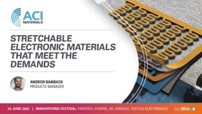
- Stretchable Electronic Materials that Meet the Demands
This is an auto-generated transcript to help the video. It has not been proof read by a person threfore they may be error Hello, everyone. I'm Andrew Baumbach. And I'm the Stretchable electronics product manager at ACI Materials. I'll do a brief overview of our our stretch portfolio and I'll start with talking a little bit about the patented cavitation processing tool that we use here to manufacture these inks. And basically what we're doing is we're harnessing the power of cavitation, which you can think of as exploding microbubbles. And it allows us to achieve levels of dispersion that conventional mixing cannot achieve. And this is all done without damaging functional fillers, which can be a problem with with some mixing technology out there. And it's a very highly controlled process and it's all automated. And this helps give excellent batch to batch consistency. And this is especially true when you're talking about carbon based materials to the particles high aspect ratio, things like carbon nanotubes, graphene, things like that that are extremely difficult to disperse. And now going into the stretch product portfolio, I'll talk about the 11 and nine. This is our silver conductor. You can think of this as the interconnects and the bus bars that are used in wearable electronics. We'll go over some of the performance data on the next slide. The SC 5025, that's the fixed resistance, stretchable heatsink. And so this is used for printing wearable heaters that heat very uniformly and you can do smaller resistors. I have an example later on of a 12 by 12 heater that we've done here and then we have the SI 1502, which is the printed carbon conductor typically used to encapsulate electrodes silver that's exposed and helps protect that while allowing access to the the conductivity. And then the AC 3104 is the stretchable insulator and that's just printed over the circuitry and that helps protect it from the environment and mechanical abrasions and has great ability. So I'm going to go over a few things that we commonly get asked here. And that's basically the stretch performance being one one big one. So here I have some graphs of our our performance. These are 76 millimeter by two millimeter. JThey all have an initial resistance of 0.9 ohms. So on the vertical here, you can kind of use that as a gauge factor as well. And on the left side, left side here on the chart. It shows the 20% stretch test which is done on fabric. So it's TPU that is bonded with an adhesive to the fabric and that stretched out 15.2 millimeters per second. So here you can see that in the performance that you start to get a nice leveling behavior and this is going out five, 5000 cycles. We have done testing hundreds of thousands of cycles and it does tend to go up a little bit, but it always recovers really nicely. And then on the right side here, we have two charts. We have a 50% stretch, 100% stretch, 550 cycles respectively. And this is just on the TPU film because for the most part, fabric doesn't go past. I think 30% is the highest stretch fabric I've seen. So this is just on TPU and this really kind of shows the performance of the ink just by itself. So you can see that although it's going up, which you can expect that it would go up if you're doing a change in length. To me, the telling thing is each cycle it's coming back down to a lower gauge factor. And in fact, if over time, as the TPU covers, it'll it'll drop closer and closer back to its original resistance. And then the 100% just kind of shows the durability of the ink. One of the key key requirements for a good stretch polymer thick film is that you can't have cracks developing while stretching. So our inks don't crack and they're highly durable. And the 100% you can see it's dropping back down, similar to how the 50% stretch did as well. So wash ability. That's another big, big question that people have. I have I have a data set here that is showing a 15 wash cycle just wash and hang dry. So this would be kind of like following the garment manufacturer's instructions. We do other tests and we'll have more data sets in the future. But this is just showing that even after washing, you get a nice flat resistance. It doesn't change over time. In the graphics here, you can see that it's the heat remains uniform and it doesn't change over the wash cycles and the power output is also stable at a 2.5 AMP test. And these are just examples of some of the applications that we see a lot of interest in. Biometric sensors got heart rate monitoring, just collecting signals from throughout the body and relaying it to a processor. And then, of course, the fix resistance heaters. We've seen a lot of interest in being washable, getting temperatures up to 140 degrees Fahrenheit. And then it's just not bulky. It doesn't have those wires and can go on to thinner base layers, things that are closer to the skin that you wouldn't necessarily want, you know, for traditional heaters, wearable heaters. And your time is almost up. And we're always interested to work with with people and new applications. And I encourage you to reach out to us and talk about your applications, and we can see what we can do for you. This is really durable ink and it has great, great potential for a lot of a lot of different areas.
- Keiron | When InkJet Doesn't Work: Deposition Via Lift Technology
This article was written in a collaboration between Keiron Printing Technologies and LMNS by Roland Biemans and originally published in Specialist Printing Worldwide: Issue Two: 2022. Contact: Marco van Hoorn Email: info@keirontechnologies.com Phone: +31 (0)40 209 7074 Laser-Induced Forward Transfer (LIFT) printing is a high precision, non-contact method of printing materials that cannot be deposited through existing print processes. Roland Biemans, Founder/Owner of LMNS, a group offering independent print industry expertise, delves into the technology and its uses. The intelligent electronic skin The printing industry is ever-expanding into new application fields. Besides long-accepted traditional processes, innovative technology paves the way toward digital and hybrid methods that allow going beyond promotional and decorative printing. In particular, where it concerns functional and industrial printing, the search for alternatives continues when screen, transfer or inkjet processes are unable to offer a solution. One such alternative is LIFT, or Laser-Induced Forward Transfer printing; a high precision, non-contact method to print materials that are too viscous, too expensive or simply too difficult to be deposited through existing print processes. "LIFT is based on the principle of using laser pulses to jet material off of a donor plate for deposition onto a receiving substrate" Inkjet is known for its versatility in various industries, notably promotional graphics and decorative printing of full-colour images, where ink formulations are tailored to mimic traditional processes, but with the characteristics to run through small printhead nozzles. Most are either dye-based or have a relatively low amount of small pigment particles as a colourant. The solid content is usually kept to a minimum to promote stability and runability. Formulations are typically based on a primary carrier such as water or oil, and additives to control the stability of the composition and process such asco-solvents, humectants, surfactants, resins and initiators. In all cases, inkjet inks are developed with the application in mind and must be compatible with the substrate they are printed upon, or with the primer or pre-treatment of the media to which the colourant will bind. It is a delicate balance between having a fluid that has the right rheology to be jetted without any issues, yet, at the same time, delivering the right wetting and drying characteristics and material quality so that once it is deposited onto the receiving surface, it will perform according to the required fastness properties. A donor plate holds the material that needs to be deposited onto the substrate. A laser pulse agitates the material to form a jet. Visit Keiron virtual booth Deposition Challenges One of the bigger challenges has been to formulate an ink that will allow the formation of droplets that have the right size, velocity, directionality and frequency when being jetted from the printhead without having solid particles eventually blocking nozzles. The emergence of recirculation printheads has greatly enhanced the bandwidth of inkjet performance and it certainly has decreased clogging issues. As such, inkjet research is increasingly directed at printing non-decorative industrial and functional fluids with higher solid particle loads or functional components such as silver, gold, copper or graphene. But what if the application requires a non-contact deposition method with ultra-high precision that surpasses inkjet capabilities? What if the particle size or solid content volume prevents proper jetting with a nozzle? And what if the cost per drop in relation to the volume of ink is so high that precision and accuracy are more important than productivity? Stacking or layering solid particles in a pattern with a positioning precision of less than five microns is not an easy feat. In an application field where, for instance, conductivity in thin lines is needed, both accuracy and precision need to be warranted to prevent circuit interruption. This deposition requirement for repeatability alone is one of the key factors in choosing a printing process. And inkjet is often not capable of successfully reaching this accuracy level; certainly not when it concerns jetting material with a viscosity of 300cP or higher, and a particle load of 50wt% or more. Figure 1: Close-up photo of a LIFT printed glass surface, using silver nanoparticle ink from PV Nano Cell. Line thickness is approx. 100 microns / 0.1mm. Visit Keiron virtual booth A viable alternative could be LIFT printing, where the solid content and the viscosity is not limited by the restrictions of a printhead. Instead of trying to tailor a fluid to the relatively narrow bandwidth of inkjet, LIFT is based on the principle of using laser pulses to jet material off of a donor plate for the deposition onto a receiving substrate. The Lift Print Process The donor plate, usually a transparent carrier substrate such as glass, quartz or fused silica, is homogeneously coated with the deposition material. This is mostly done by spin-coating or blade-coating. The donor material can be solid, fluid or paste. The donor plate is positioned directly above the receiving substrate, which can be a flexible foil, a rigid media, or any other object such as a panel, a machine component or (semi-) finished product. A laser beam is focused on the donor layer and a pulse initiates a gas pocket that expands to form a jet. Depending on the type and combination of laser beam and optics, the dot diameter, pulse frequency and intensity are configured. Jetting speeds depend on the LIFT system set-up; the example used in this article (see Figure 1) is printed by Eindhoven-based Keiron Printing Technologies with a firing frequency of up to 300kHz with a single laser beam jetting a dot diameter of 100 microns. "Stacking or layering solid particles in a pattern with a positioning precision of less than five microns is not an easy feat" Where inkjet typically uses one and the same ink formulation in a system set-up and a preset print mode (single-pass/multi-pass, resolution/drop-size, dithering/screening, etc.), LIFT allows for the exchange of donor plates and variable donor materials in the same production run. Stacking or layering of different fluids and materials using the same deposition technology opens up possibilities for a hybrid printing approach. Complex patterns and structures can be printed at high speed and high precision. The quality of the deposition depends on the quality of the donor plate coating. Visit Keiron virtual booth Application Fields Although LIFT seems promising, it has been, to a large extent, a niche technology slow to gain traction with a wider audience. The technique is not new: in fact, in the late 1960s, the first patent describing the operating principle of LIFT was filed. In the 1980s LIFT as an acronym was coined and the process was tested as a novel technology to deposit metals and oxides. "LIFT has seen successful application uses for the deposition of inorganic, organic and living material" By now, LIFT has seen successful application uses for the deposition of inorganic, organic and living material. For medical and pharmaceutical application fields, bioprinting is an area of interest, with possibilities in cell tissue engineering and protein deposition. Moreover, printed electronics is an application field that LIFT has been tested on extensively. Think sensors, antennas and solar cells, for instance. Due to its non-contact, high-precision, high-speed jetting performance, LIFT is a promising printing technology that enables deposition of viscous and precious material. Video still: LIFT uses laser pulses to jet material off of a donor plate and deposit in onto a receiving substrate. Visit Keiron virtual booth At the ESMA IPI conference taking place 18–19 May 2022 in Düsseldorf, Keiron will showcase its technology platform and the various application fields it has been researching. As part of the HighTechXL deep tech venture building programme in Brainport Eindhoven, with partners such as TNO Holst Centre, Keiron started off with the intention to create a platform for the production of ‘lab on a chip’ devices. More recently, the start-up company has secured funding allowing it to build its first alpha tool. Innovations Festival: Printed, Hybrid, 3D, InMold, Textile Electronics 24 June 2022 | 13:00 - 19:00 CET | Virtual Event Platform Keiron will be having a virtual booth at the Innovation Festival. Visit Keiron virtual booth
- Real World Smart Packaging For Pharmaceuticals
Speaker: Michael Petersen | Company: Information Mediary Corporation| Date: 10-11 March 2021 | Full Presentation Bio Michael is a sought after presenter at conferences and has taught master class sessions on digital health transformation, NFC/RFID, coldchain, and printed electronics, smart packaging in Europe, Asia and North America. Michael has co-founded and shaped IMC (Information Mediary Corp) into the world’s leading smart-package and medication adherence solutions provider. Experience the power of convergence with our connected smart packaging and innovative, patient centric adherence solutions. Our solutions run over global health platforms to connect patients and their data directly with their care teams to assist in behavioural modification and support both AI and human clinical decisions. www.informationmediary.com Join TechBlick on an annual pass to join all live online conference or online version of onsite conference access library of on-demand talks (600 talks + PDFs) portfolio of expert led masterclass year-round platform https://www.techblick.com/ And do NOT miss our flagship event in Berlin on 17-18 OCT 2023 focused on Reshaping the Future of Electronics. This event attracts 550-600 participants from all the world and offers a superb ambience and dynamic exhibition floor. To learn more visit https://www.techblick.com/electronicsreshaped To see feedback about previous event see https://www.techblick.com/events-agenda