Search Results
Search this site
1075 results found with an empty search
- R2R Printed Carbon Nanotube TFT Sheets
Speaker: Patrick Malenfant | Company: National Research Council Canada (NRCC) | Date: 10-11 March 2021 | Full Presentation This presentation covers our progress in high purity semiconducting single-walled carbon nanotube (sc-SWCNT) enrichment and transistor fabrication via solution based processes. I will highlight our recent progress in understanding sc-SWCNT enrichment using conjugated polymers (isolation of high purity sc-SWCNT), with special consideration given to the effects of solvent parameters and doping on the yield/purity of the final product. Fully printed transistors combining R2R gravure and inkjet-printing will be described as well as our recent progress in realizing “limitless” R2R gravure printed TFT backplanes capable of driving an e-paper display. Patrick R. L. Malenfant*(1), Jianfu Ding(1), Jianying Ouyang(1), Zhao Li(1), Chang Guo(1), Jacques Lefebvre(1), Paul Finnie(1), Francois Lapointe(1), Gyoujin Cho(2) (1)National Research Council Canada, 1200 Montreal Road, Ottawa, ON, K1A 0R6, Canada. (2)Dept. of Biophysics, Sungkyunkwan University (SKKU), South Korea Patrick Malenfant Director of Research Development @ National Research Council Canada (NRCC) Bio Dr. Patrick Malenfant studied chemistry at the University of Ottawa (BSc 1995), Cornell University (MSc 1997), and the University of California - Berkeley (PhD 2000). He has 10 years of industrial R&D experience including a one year postdoc at IBM's TJ Watson Research Center and 9 years at the GE Global Research Center where he developed nanomaterials for Aerospace, Healthcare, and Organic Electronics applications. He joined the National Research Council of Canada in 2010 as a Senior Research Officer. He is currently the Director of R&D in the Security and Disruptive Technologies Research Center overseeing activities in Quantum Science, Printed Electronics and Structural Materials. Join TechBlick on an annual pass to join all live online conference or online version of onsite conference access library of on-demand talks (600 talks + PDFs) portfolio of expert led masterclass year-round platform https://www.techblick.com/ And do NOT miss our flagship event in Berlin on 17-18 OCT 2023 focused on Reshaping the Future of Electronics. This event attracts 550-600 participants from all the world and offers a superb ambience and dynamic exhibition floor. To learn more visit https://www.techblick.com/electronicsreshaped To see feedback about previous event see https://www.techblick.com/events-agenda
- Commercial Ready High Energy Density Ultra-Fast Charge Cells
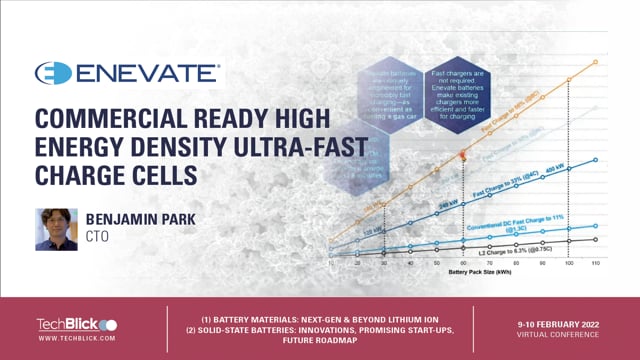
Speaker: Benjamin Park | Company: Enevate Corporation | Date: 9-10 Feb 2022 | Full Presentation Why bother with fast charge for EV batteries? Charge rate goes beyond driver convenience - it addresses core EV adoption issues such as addressing the fact that only 20% of cars have access to overnight charging, fast charging helps improve existing infrastructure utilization, and it supports drivers becoming more comfortable with less expensive vehicles that have shorter range lowering the price for those vehicles. Enevate is a battery technology company supplying breakthrough Extreme Fast Charge Technology with its pure silicon-dominant cells that are solving these crucial EV adoption issues. Join TechBlick on an annual pass to join all live online conference or online version of onsite conference access library of on-demand talks (600 talks + PDFs) portfolio of expert led masterclass year-round platform https://www.techblick.com/ Our next battery-related event will take place on 15-16 FEB 2023, covering 1) Solid-State Batteries: Innovations, Promising Start-Ups, & Future Roadmap 2) Battery Materials: Next-Generation & Beyond Lithium Ion The speakers include: General Motors, Graphenix Development, Brookhaven National Laboratory, Fraunhofer IKTS, RWTH Aachen University, Lawrence Livermore National Laboratories, Meta Materials Inc, Skeleton Technologies, Solid State Battery Inc, Argonne National Laboratories, OneD Battery Sciences, VTT, Leyden Jar Technologies B.V., b-Science, Rho Motion, Wevo-Chemie, LiNA Energy, CNM Technologies, Ionblox, Empa, Zinc8 Energy Solutions, Avicenne Energy, Echiontech, South8 Technologies, Basquevolt, NanoXplore, Chasm, Li Metal, Sila Nanotechnologies, Quantumscape (tentative), Fraunhofer ISI, etc https://www.techblick.com/
- Flexible thin-film loudspeaker
MIT engineers have developed a paper-thin loudspeaker that can turn any surface into an active audio source. This thin-film loudspeaker produces sound with minimal distortion while using a fraction of the energy required by a traditional loudspeaker. The hand-sized loudspeaker the team demonstrated, which weighs about as much as a dime, can generate high-quality sound no matter what surface the film is bonded to. To achieve these properties, the researchers pioneered a deceptively simple fabrication technique, which requires only three basic steps and can be scaled up to produce ultrathin loudspeakers large enough to cover the inside of an automobile or to wallpaper a room. Used this way, the thin-film loudspeaker could provide active noise cancellation in clamorous environments, such as an airplane cockpit, by generating the sound of the same amplitude but opposite phase; the two sounds cancel each other out. The flexible device could also be used for immersive entertainment, perhaps by providing three-dimensional audio in a theater or theme park ride. And because it is lightweight and requires such a small amount of power to operate, the device is well-suited for applications on smart devices where battery life is limited. “It feels remarkable to take what looks like a slender sheet of paper, attach two clips to it, plug it into the headphone port of your computer, and start hearing sounds emanating from it. It can be used anywhere. One just needs a smidgeon of electrical power to run it,” says Vladimir Bulović, the Fariborz Maseeh Chair in Emerging Technology, leader of the Organic and Nanostructured Electronics Laboratory (ONE Lab), director of MIT.nano, and senior author of the paper. Bulović wrote the paper with lead author Jinchi Han, a ONE Lab postdoc, and co-senior author Jeffrey Lang, the Vitesse Professor of Electrical Engineering. The research is published today in IEEE Transactions of Industrial Electronics. A new approach A typical loudspeaker found in headphones or an audio system uses electric current inputs that pass through a coil of wire that generates a magnetic field, which moves a speaker membrane, that moves the air above it, that makes the sound we hear. By contrast, the new loudspeaker simplifies the speaker design by using a thin film of a shaped piezoelectric material that moves when voltage is applied over it, which moves the air above it and generates sound. Most thin-film loudspeakers are designed to be freestanding because the film must bend freely to produce sound. Mounting these loudspeakers onto a surface would impede the vibration and hamper their ability to generate sound. To overcome this problem, the MIT team rethought the design of a thin-film loudspeaker. Rather than having the entire material vibrate, their design relies on tiny domes on a thin layer of piezoelectric material which each vibrate individually. These domes, each only a few hair widths across, are surrounded by spacer layers on the top and bottom of the film that protect them from the mounting surface while still enabling them to vibrate freely. The same spacer layers protect the domes from abrasion and impact during day-to-day handling, enhancing the loudspeaker’s durability. To build the loudspeaker, the researchers used a laser to cut tiny holes into a thin sheet of PET, which is a type of lightweight plastic. They laminated the underside of that perforated PET layer with a very thin film (as thin as 8 microns) of piezoelectric material, called PVDF. Then they applied a vacuum above the bonded sheets and a heat source, at 80 degrees Celsius, underneath them. Because the PVDF layer is so thin, the pressure difference created by the vacuum and heat source caused it to bulge. The PVDF can’t force its way through the PET layer, so tiny domes protrude in areas where they aren’t blocked by PET. These protrusions self-align with the holes in the PET layer. The researchers then laminate the other side of the PVDF with another PET layer to act as a spacer between the domes and the bonding surface. “This is a very simple, straightforward process. It would allow us to produce these loudspeakers in a high-throughput fashion if we integrate it with a roll-to-roll process in the future. That means it could be fabricated in large amounts, like wallpaper to cover walls, cars, or aircraft interiors,” Han says. High quality, low power The domes are 15 microns in height, about one-sixth the thickness of a human hair, and they only move up and down about half a micron when they vibrate. Each dome is a single sound-generation unit, so it takes thousands of these tiny domes vibrating together to produce audible sound. An added benefit of the team’s simple fabrication process is its tunability — the researchers can change the size of the holes in the PET to control the size of the domes. Domes with a larger radius displace more air and produce more sound, but larger domes also have lower resonance frequency. The resonance frequency is the frequency at which the device operates most efficiently, and a lower resonance frequency leads to audio distortion. Once the researchers perfected the fabrication technique, they tested several different dome sizes and piezoelectric layer thicknesses to arrive at an optimal combination. They tested their thin-film loudspeaker by mounting it to a wall 30 centimeters from a microphone to measure the sound pressure level, recorded in decibels. When 25 volts of electricity were passed through the device at 1 kilohertz (a rate of 1,000 cycles per second), the speaker produced high-quality sound at conversational levels of 66 decibels. At 10 kilohertz, the sound pressure level increased to 86 decibels, about the same volume level as city traffic. The energy-efficient device only requires about 100 milliwatts of power per square meter of speaker area. By contrast, an average home speaker might consume more than 1 watt of power to generate similar sound pressure at a comparable distance. Because the tiny domes are vibrating, rather than the entire film, the loudspeaker has a high enough resonance frequency that it can be used effectively for ultrasound applications, like imaging, Han explains. Ultrasound imaging uses very high-frequency sound waves to produce images, and higher frequencies yield better image resolution. The device could also use ultrasound to detect where a human is standing in a room, just like bats do use echolocation, and then shape the sound waves to follow the person as they move, Bulović says. If the vibrating domes of the thin film are covered with a reflective surface, they could be used to create patterns of light for future display technologies. If immersed in a liquid, the vibrating membranes could provide a novel method of stirring chemicals, enabling chemical processing techniques that could use less energy than large batch processing methods. “We have the ability to precisely generate mechanical motion of air by activating a physical surface that is scalable. The options of how to use this technology are limitless,” Bulović says. “I think this is a very creative approach to making this class of ultra-thin speakers,” says Ioannis (John) Kymissis, Kenneth Brayer Professor of Electrical Engineering and Chair of the Department of Electrical Engineering at Columbia University, who was not involved with this research. “The strategy of doming the film stack using photolithographically patterned templates is quite unique and likely to lead to a range of new applications in speakers and microphones.” This work is funded, in part, by the research grant from the Ford Motor Company and a gift from Lendlease, Inc. For more information, visit: https://news.mit.edu/2022/low-power-thin-loudspeaker-0426
- AGENDA: Graphene, CNTs & 2D Materials. Users, Applications, Major Producers & Start-Ups
26 - 27 April 2022 | 14:00 - 21:20 CET | Virtual Event Platform Add Event to your Calendar Google Calendar | Microsoft Outlook Calendar | Office 365 Calendar | Yahoo Calendar TechBlick’s event on 26-27 April 2022 covers the full spectrum of Graphene, CNT, and 2D material-technical innovations, industrial progress, and application development. TechBlick brings together a handpicked world-class agenda consisting of end-users, manufacturers, promising start-ups, as well as renowned market analyst groups. Agenda Topics Covered: Graphene | Carbon Nanotubes (SWCNT, MWCNTs) | Boron Nitride | 2D Materials | Boron Nitride | Graphene-Silicon Anode | Battery Additives | Supercapacitors | Biosensors | Concrete and Cement Additives | Filtration Membranes | Composites and Plastic Additives | Fibers and Advanced Textiles | Gas Sensors | Memory Devices | Shielding | Conductive Fibers | Scale-Up | Quantum Electronics | Reflective Displays | Speaker Membranes and Transducers | Anti-Corrosion Coatings and Additives | Novel Manufacturing Methods | Functionalization | R2R CVD Growth and Transfer | Venture Capital Investment | Wafer Based Electronics
- Embedded Metal Mesh as Highly Transparent Conductive Film and Heaters
Speaker: Zheng Cui | Company: Printable Electronics Research Center China| Date: 10-11 March 2021 | Full Presentation A hybrid printing approach is presented for making embedded metal mesh as transparent conductive film, with the lowest sheet resistance of 0.03ohm/sq. while still maintaining 86% transparency. Roll-to-roll mass manufacturing of the metal mesh transparent conductive films have been realized for touch panels which have been commercialized in a number brand name display devices. The high surface conductivity of embedded metal mesh also opened up a number other applications in addition to touch panels, such as transparent EMI shielding, transparent heating, wearable thermal healing and high density flexible circuits, etc. Join TechBlick on an annual pass to join all live online conference or online version of onsite conference access library of on-demand talks (600 talks + PDFs) portfolio of expert led masterclass year-round platform https://www.techblick.com/ And do NOT miss our flagship event in Berlin on 17-18 OCT 2023 focused on Reshaping the Future of Electronics. This event attracts 550-600 participants from all the world and offers a superb ambience and dynamic exhibition floor. To learn more visit https://www.techblick.com/electronicsreshaped To see feedback about previous event see https://www.techblick.com/events-agenda
- Networking Break - Meet The Speakers In The Lounge
Company: Break | Date: 9-10 Feb 2022 | Full Presentation Join TechBlick on an annual pass to join all live online conference or online version of onsite conference access library of on-demand talks (600 talks + PDFs) portfolio of expert led masterclass year-round platform https://www.techblick.com/ Our next battery-related event will take place on 15-16 FEB 2023, covering 1) Solid-State Batteries: Innovations, Promising Start-Ups, & Future Roadmap 2) Battery Materials: Next-Generation & Beyond Lithium Ion The speakers include: General Motors, Graphenix Development, Brookhaven National Laboratory, Fraunhofer IKTS, RWTH Aachen University, Lawrence Livermore National Laboratories, Meta Materials Inc, Skeleton Technologies, Solid State Battery Inc, Argonne National Laboratories, OneD Battery Sciences, VTT, Leyden Jar Technologies B.V., b-Science, Rho Motion, Wevo-Chemie, LiNA Energy, CNM Technologies, Ionblox, Empa, Zinc8 Energy Solutions, Avicenne Energy, Echiontech, South8 Technologies, Basquevolt, NanoXplore, Chasm, Li Metal, Sila Nanotechnologies, Quantumscape (tentative), Fraunhofer ISI, etc https://www.techblick.com/
- Current Applications and Outlook of 3D Printed Electronics
Speaker: Valentin Storz | Company: NanoDimension| Date: 10-11 March 2021 | Full Presentation The presentation discusses current applications and outlook for the new production technology with focus on Nano Dimensions AME Technology. Nano Dimension (Nasdaq: NNDM) is a provider of intelligent machines for the fabrication of Additively Manufactured Electronics. Customer cases form Hensoldt (DE), CBN-IIT (IT), L3Harris (US), Rehau (DE), UTS (AU) with Applications in the field of Rapid Prototyping of complex PCB, 3D Electronics, Sensors, Heterogeneous Integration and SiP and RF applications are presented. Join TechBlick on an annual pass to join all live online conference or online version of onsite conference access library of on-demand talks (600 talks + PDFs) portfolio of expert led masterclass year-round platform https://www.techblick.com/ And do NOT miss our flagship event in Berlin on 17-18 OCT 2023 focused on Reshaping the Future of Electronics. This event attracts 550-600 participants from all the world and offers a superb ambience and dynamic exhibition floor. To learn more visit https://www.techblick.com/electronicsreshaped To see feedback about previous event see https://www.techblick.com/events-agenda
- NFC & UHF Flexible & Hybrid Sensor Tags
Speaker: Thomas Germann | Company: IDENTIVE | Date: 11-12 May 2021 | Full Presentation Bio Thomas Germann joined Identiv in 2013 in the R&D department of Identiv’s RFID transponder & reader business unit and is now its R&D Manager. He is mainly responsible for development of novel UHF & HF RFID tags, as well as Sensor-enabled NFC products with functionality beyond pure identification. Thomas brings a strong background in RFID label and printed electronics product development, which enable the development of cutting edge flexible RFID & NFC sensor tags and corresponding systems. Thomas holds a Diploma (M.Sc.) in Engineering Physics from the Technische Universität München (TUM). Join TechBlick on an annual pass to join all live online conference or online version of onsite conference access library of on-demand talks (600 talks + PDFs) portfolio of expert led masterclass year-round platform https://www.techblick.com/ And do NOT miss our flagship event in Berlin on 17-18 OCT 2023 focused on Reshaping the Future of Electronics. This event attracts 550-600 participants from all the world and offers a superb ambience and dynamic exhibition floor. To learn more visit https://www.techblick.com/electronicsreshaped To see feedback about previous event see https://www.techblick.com/events-agenda
- Welcome & Introduction
Speaker: Khasha Ghaffarzadeh | Company: TechBlick | Date: 9-10 Feb 2022 | Full Presentation Join TechBlick on an annual pass to join all live online conference or online version of onsite conference access library of on-demand talks (600 talks + PDFs) portfolio of expert led masterclass year-round platform https://www.techblick.com/ Our next battery-related event will take place on 15-16 FEB 2023, covering 1) Solid-State Batteries: Innovations, Promising Start-Ups, & Future Roadmap 2) Battery Materials: Next-Generation & Beyond Lithium Ion The speakers include: General Motors, Graphenix Development, Brookhaven National Laboratory, Fraunhofer IKTS, RWTH Aachen University, Lawrence Livermore National Laboratories, Meta Materials Inc, Skeleton Technologies, Solid State Battery Inc, Argonne National Laboratories, OneD Battery Sciences, VTT, Leyden Jar Technologies B.V., b-Science, Rho Motion, Wevo-Chemie, LiNA Energy, CNM Technologies, Ionblox, Empa, Zinc8 Energy Solutions, Avicenne Energy, Echiontech, South8 Technologies, Basquevolt, NanoXplore, Chasm, Li Metal, Sila Nanotechnologies, Quantumscape (tentative), Fraunhofer ISI, etc https://www.techblick.com/
- How Does Speed Networking Work In Our Unique Platform?
We also plan special speed networking activities where you can meet many people in rapid succession, make brief introductions, and exchange business details. Click on the video below to see how it works.
- CondAlign | Adhesive ACF for efficient room temperature bonding in FHE | June 2022
This is an auto-transcribed version without human control Fantastic. So thank you for the introduction. Lindbergh is my name Cornelis. It's a company based in Oslo making anisotropic conductive film. So what we provide is an electrical and mechanical interconnection by this adhesive anisotropic conductive film, which enables bonding at the room temperature and finger pressure. So no curing. You get the film from us in the form of a double sided tape, which you can bond your components with. With the the advantage with the film is that you retain the original polymer properties much better because we use much less conductive film fillers than in conventional conductive films. That is due to our on the line alignment process, which I'm not going to go into today. But also you have heard me before. I know about this this process. It's also enables a very flexible product design. In principle, it is material independent, as I said, which opens for development or tailor made application based products. So where are we today with the product pipeline? We are in the moment though qualifying and qualified qualify and verify the first time, which we call the line 100, which is the thickness of 100 micrometer. Also, the pitch between the conductive chains is also about 100 micrometer. Typical application areas which we work quite a lot with. The paper battery is coming up now smart labels connections with similar pad sizes, which is more than like in the area to hundred, about 200 micrometers, which is quite large for us. So I'll come back to to the sizes afterwards. This is in verification and is in the qualification product with several customers now. And we we expect to run this from our roll to roll line here in Oslo before the end of this year in in commercial quantities, which for us will say up to 10,000 square meters annually from our machine supply about that get will come from from OEM manufacturers that we contract next product in the light will be what we call new line 35 or 40 in that area. It's not completely defined yet. Pitch then will be in the area of 34 three micrometer thickness as well. And this is typically the applications with cheap bonding and other connection with the smaller pad sizes. This is next in line for the first product. I meant I mentioned the come then later this year or next year for future products, we're talking about 15 or something, 1050 micrometer thickness and pitch. So here you have a little about the pitch sizes. So this green, this is this area on the left side, the TEC one is a E line 100 with typical sizes as you see here, 200 by 2000 micrometer at the top thousand by 2300 by 600 400 by five. That's typical pad sizes for these applications. And we go up to the top right. You see that what we call the take two will be the second product, which then go more to typical ICI connections. And though not the right to see the the future applications are very high density and then we are actually talking about components of our micro LEDs and those small components down to like in the area of 20 micrometer by 20 micrometer. So manufacturing is a role. The role one production technology. I say multiple products and applications. The picture on the top right is actually our machine here in Oslo. And when you say the industrial production strategy is that we make interim production here in Oslo and qualify the processes, and we come up over to column two. It's contract manufacturing for for higher volumes. And we can also discuss licensing license manufacturing. If you are a high volume customer who want to include this process in your and your internal production lines down to the right, you see some very schematic picture of the process itself. Two words about the time we are then a company based in Oslo developing and making anisotropic conductive films. The product focus is, as I say, ICF, as I mentioned here, and we also use the same process technology for making thermal interface materials.
- Kent Displays | VersaNote: A Roll-to-Part, Flexible Electronic Device | June 2022
This is an auto-transcriped presentation without any human control So I'm here to talk about Versanote, which is a roll to part flexible electronic device. So thank you for allowing me to talk to you. Versa note is made by Boogie Board, which is a brand by Kent displays. We're experts in reflective by stable call history technology and our mission is really to redefine the writing experience through both technology and design. We've been around since 1993 and we have about 75 employees. We've been making boogie boards for about 12 years, and we've expanded our product into a variety of markets from if you're looking at the slide up or left hand corner as toys down through the middle as toys going back up through the center is educational products moving over to our job and dashboard lines, which are more general purpose to our versa note line and onto our Blackboard line, which is used for high end office applications for the versa note development. It's a little bit different than our regular boogie board. It's kind of a departure. So really our process that we use to, to, to develop it was based on the idea of let's make our writing surface flexible, and then we process through some feasibility steps, some prototype steps and finally scale up and then to manufacturing. So a little bit about the versa. Note Its functionality is very similar to the boogie board where the liquid crystal flows and response to pressure and reflects a bright line. But here the surface is flexible and also it electronically erases and is ready to be used again and again like a boogie board. And some of the advantages we think is it's it's a fun, unique writing experience that's that's different than writing on a, a tablet or on paper, because it can be used over and over again. We see it as a replacement for paper, and it can be used for games or notes or just jotting down information before you lose your thought. And from a mass production standpoint, it's made by clean room based roll to part processes. And here's some pictures showing some of the typical use of it for jotting down notes it has especially formed corner that allows you to pick up the device and handle it. And I want to draw your attention to the figure at the bottom that shows the stylus. It's a special stylus that if you you can write on it in one side. And when you turn over and use the end of the stylus and center that over the circular area on the versa note it will be it will erase and be ready ready to be used again as we were developing the unique manufacturing processes for making versa note we decided to offer these these assets and our expertise to others through a contract manufacturing service called Technical Services. So some of the technical services that we offer are we have about 12,000 square feet of manufacturing space that houses three clean room based roll to roll manufacturing lines. And we have a suite of chambers, as well as optical and dimensional metrology systems. The things that differentiate us from others are we do clean room based manufacturing and we do pilot to high volume. We have very automated manufacturing and we do product and process development. So for some things, we've had to bring in new processes and develop them. And we are based in in beautiful Kent, Ohio. Some of the manufacturing competencies I'd like to highlight are, are those that are used in versa note and also available to others through our tech services division is the lamination of optical optical optically clear adhesives as well as pressure sensitive adhesives, the printing of decorative and functional materials and even printing patterned pieces like the might be used for membrane switches. And then we have a variety of simulation options, which is how we go from a roll of film to a part. We do multi axis precision rotary dye cutting so we can print something and then die cut to that print. And we also do roll to roll laser cutting and and processing. And then we also have electrical assembly, low pressure injection molding as well as custom packaging. So kind of talking a little bit about the technical services process, it's really to listen to the customer, develop some plan to demonstrate feasibility, take that to the next step for prototyping and then scaling that up. Where you get to initial production and problem solving and finally to manufacturing. So that's a little bit about versa note and a little bit about our technical services division. I'd be happy to answer any questions or here's my contact info. Please reach out to me. I'd love I'd love to talk to you about either one. So thank you very much.