Search Results
Search this site
1084 results found with an empty search
- Taking the accuracy of printed electronics below 1um
Printed electronics technology is evolving. A development direction is ultrafine line printing, increasingly allowing the technology to encroach into the realm of photolithography. The example here, developed by VTT, demonstrate a process for sub-micron printing. The process is reverse offset printing. Here, the PDMS roller is first coated with the ink. The ink semi-dries on the roller, partially through absorption into the PDMS. This semi-dried state allows one to overcome wetting-related issues when inks are in liquid state. The inked PDMS roller is brought into contact with a Cliche, or relief plate, removing parts of the inks. The patterned semi-dried inks on the PDMS roller are then transferred onto the final substrate. In this example VTT achieves 1µm direct printing of silver nanoparticle inks. The desktop RO printer was used to print a metal mesh on PET with 1µm linewidths. The reported sheet resisitivty is not very low (100Ohm/sqr), probably because the lines are very thin. In general, note that ROP can enable minimum resolutions between 0.5-5µm, printed thickness lines around 20-1000nm, overlay accuracy <2um, and printing speeds of 50mm/s (3m/min).
- Micro to Giga Scale: Different Materials, Processes and Challenges
Speaker: Denis Pasero | Company: Ilika | Date: 9-10 Feb 2022 | Full Presentation Solid State Batteries are expected to outperform incumbent liquid-based battery technologies thanks to potential safety and performance advantages. SSBs have the potential to improve and even enable new application over a wide Wh-level range: from micro-batteries powering Augmented Reality smart contact lenses and perpetual Internet of Things sensors; to pouch cells providing safer and lighter power to cordless domestic devices and longer range to electric vehicles and new aerospace applications. Yet, after a few decades of R&D, the commercialisation of small SSB is only recent and that our larger format pouch cells still around the corner. This presentation will compare and contrast the various challenges and choices of chemistries, processes and engineering solutions necessary for the development of mWh level micro batteries to the full commercialisation of SSB modules at GWh level. Join TechBlick on an annual pass to join all live online conference or online version of onsite conference access library of on-demand talks (600 talks + PDFs) portfolio of expert led masterclass year-round platform https://www.techblick.com/ Our next battery-related event will take place on 15-16 FEB 2023, covering 1) Solid-State Batteries: Innovations, Promising Start-Ups, & Future Roadmap 2) Battery Materials: Next-Generation & Beyond Lithium Ion The speakers include: General Motors, Graphenix Development, Brookhaven National Laboratory, Fraunhofer IKTS, RWTH Aachen University, Lawrence Livermore National Laboratories, Meta Materials Inc, Skeleton Technologies, Solid State Battery Inc, Argonne National Laboratories, OneD Battery Sciences, VTT, Leyden Jar Technologies B.V., b-Science, Rho Motion, Wevo-Chemie, LiNA Energy, CNM Technologies, Ionblox, Empa, Zinc8 Energy Solutions, Avicenne Energy, Echiontech, South8 Technologies, Basquevolt, NanoXplore, Chasm, Li Metal, Sila Nanotechnologies, Quantumscape (tentative), Fraunhofer ISI, etc https://www.techblick.com/
- Ultrafine printed electronics: technologies for reaching sub-micron feature sizes
Printed electronics technology is evolving. A development direction is ultrafine line printing, increasingly allowing the technology to encroach into the realm of photolithography. In this article, we discuss analogue direct as well as hybrid printing technologies, bringing printed electronics into the few micron and sub-micron feature size range. This is an important development, taking printed electronics closer to electronic applications. In a subsequent article, we will cover digital printing techniques. This article is based upon recent presentations and discussions at TechBlick events. TechBlick is the home of the global printed electronics industry, providing year-round online and onsite world-class conferences, masterclasses, and industry updates. Join TechBlick on an annual or monthly annual pass to connect with the global printed electronics community (www.TechBlick.com). Our next Printed Electronics event will be an online Innovations Festival taking place on 24 June 2022. This article begins with screen printing, as it is the powerhouse of the industry. Without the exception of displays, most printed electronics applications rely upon this technology. Today, many regularly print ca. 50µm linewidths in production on flexible substrates. However, the state-of-the-art is already pushing below this limit. Here, I show two interesting examples. The right image is from Fraunhofer ISE (2019), showing how they could screen print 19µm wide lines on silicon solar cells to act as narrow fingers. This is an important advancement compared to the common >30µm linewidths, reducing Ag content per wafer and leaving more solar wafer real estate open to the sun. These are critical drivers in optimising cost and performance of silicon photovoltaics. The images in the middle (above), by Asada Mesh (2022), demonstrate printed lines on PET with linewidths as narrow as 22µm. This is not an easy feat, and require optimization of the substrate, mesh, screen, paste, etc. A key enabling technology here is ultranarrow stainless steel meshes. Here, on the right, you can see 9µm mesh wires, recently announced by Asada Mesh, showing how mesh technology is evolving. These two examples demonstrate once again that screen printing has not reached the end of the road. One underestimates this technology at one’s peril. Incremental but important improvements will soon enable S2S sub-25µm and sub-20µm linewidths on PET and wafer/ceramic substrates. The exact linewidth limit is not known, but is, for now, assumed to around 15µm. To overcome linewidth limitations of direct screen printing, hybrid solutions are proposed. These typically involve the screen printing of a moderately narrow line followed by laser or other patterning. Here, I outline the solution developed by Toray. The approach is shown schematically below. A photo-patternable screen printable paste is developed, which can be directly photolithographically patterned without requiring an additional photoresist deposition and development step. The low-temperature PET-compatible version of this paste enables L/S as narrow as 10/10 µm. However, the achieved conductivity is not the highest (around 30-80 uOhm.cm when cured at 140C). The high-temperature version of course goes higher in conductivity, approaching x2bulk (3uOhm.cm) when sintered at 850C. This solution is particularly suited to touch screen edge electrodes based on ITO on PET substrates since (a) it enables narrow edge electrodes (lower L/S) and (b) ITO film patterning requires photolithography in any case. This approach can be finetuned to support even narrower L/S. In this example, you can see fine circuit wiring and metal mesh examples, reaching 8µm and 2.5µm linewidth, respectively. Note that at 2.5µm linewidth, this hybrid printing process approaches the best-in-class metal mesh linewidths. This technology still has some limitations though, namely, a high curing temperature of 230C, (which is not PET, PEN, PC compatible) and only a moderate paste resistivity. There are many reasons why one may want to print using a technique other than screen including higher print web-speeds, finer feature sizes, and lower print thicknesses. These two charts, developed by Eastman Kodak, offer an insightful map. The left chart shows that flexo, gravure, and inkjet are better suited in forming thinner lines using lower viscosity inks. The right chart shows that inkjet, flex, and various mico-nano contact printing processes enable features sizes in the sub-30µm territory. Kodak has further advancement the art of high-speed flexographic printing of functional layers. In particular, their flexographic plates with flat top dots and high resolutions (achieved with well-designed non-Gaussian lasers) enables finer features. Here, on the left, an example of a flat top dot plate can be seen. In the right, an example of fine line printing is demonstrated for an RF antenna application. Here, a thin catalytic layer is flexographically printed and then Cu plated to achieve high bulk-like copper conductivity, required for good antenna performance. The printed linewidth can be as narrow as 7.8µm, demonstrating the fine line printing capability of this process. Below is an example of a gravure offset process developed by Komura Tech in Japan, directly printing continuous unbroken lines with sub-5um linewidth. Note that it is an ‘offset’ process, and as we will see, most sub-5um printing techniques involve an ‘offset’ step. Here the inked gravure roll first transfers the paste onto a blank role, which then transfer it onto the substrate. One advantage of this approach is that the ink can be partially dried before reaching the substrate, thus preventing wetting-related issues which limit linewidth capability. This technology enables fine metallization of circuits on flexible substrates. The lines are currently based on Ag NPs and are likely to be very thin (250-300nm). Below is another example of ‘offset’ based printing, Shashin Kagaku in Japan, demonstrated S2S direct printing of thin (250nm) layers of Ag nanoparticle inks with linewidths as narrow as 1.5µm in complex patterns. The process can be on glass and PET (note: influences also the achieved sheet resistivity due to difference in allowed curing temperature). An obvious target market is metal mesh TCFs and here they can demonstrate 0.2- 0.3 Ohm/sqr sheet resistance at 150C (PET compatible range). Here is yet another example of ‘offset’ based printing developed by VTT (Finland). In this reverse offset process, the PDMS roller is first coated with the ink. The ink semi-dries on the roller, partially through absorption into the PDMS. This semi-dried state allows one to overcome wetting-related issues when inks are in liquid state. The inked PDMS roller is brought into contact with a Cliche, or relief plate, removing parts of the inks. The patterned semi-dried inks on the PDMS roller are then transferred onto the final substrate. In this example VTT achieves 1µm direct printing of silver nanoparticle inks. The small-sized RO printer was used to print a metal mesh on PET with 1µm linewidths. The reported sheet resistivity is not very low (100Ohm/sqr), probably because the lines are very thin. Note that ROP can enable minimum resolutions between 0.5-5µm, printed thickness lines around 20-1000nm, overlay accuracy <2um, and printing speeds of 50mm/s (3m/min). In all the examples demonstrated thus far, a printed conductor (mainly Ag NP ink) is printed. However, this ultrafine line printing process can also print photoresist, enabling one to replace photolithography in some cases. The final direct ultrafine line printing process I wish to highlight is by Asahi Kasei. Here, sub-1µm unbroken straight as well as shaped lines are demonstrated. For example, in the right image, one can see a continuous 300nm wide lines, as well as TFT patterns printed for 2000 ppi (pixel per inch) resolution [here, the entire TFT pixel pitch is 12.5um) The exact process is not disclosed, but our guess is that it is a R2R reverse offset process. Here, as the case before, an ink system applies the ink onto a blanket roller. A roller mold containing the final pattern is brought into contact with the inked blanket roller, removing parts of the ink to form the pattern. Finally, the blanket roller transfers the pattern onto the final substrate. A key technology step here is in the formation of the roller, which essentially enables R2R nanoimprinting. Here, no laser is deployed. Instead, an electron beam lithography (with multiple exposure lines) is used to create ultrafine features. In the case, the roller is first dip coated, exposed to EB, developed and backed. The accuracy of this process is shown in the middle pictures, demonstrating 1µm linewidths in 5µm pitches. Currently, the rollers is available in 250mm width and 100mm diameter size or smaller. Our guest is that the current web speed is 1m/min or slower. Asahi Kasei is targeting TFT backplane metallization as well as transparent RFID antennas. Transparent RFIDs enable ones to print graphics on all parts of the package since they block no area. This narrow-line printing technique can also have security applications. So far we covered direct printing (except for screen printing). Many ‘hybrid’ solutions are also developed to enable ultrafine line features. This example is by Panasonic, although many others such as O-Film developed similar technologies before. We select the Panasonic example because it is a technically sophisticated solution, achieving 2µm features on both sides of the PET film. In this approach, fine grooves are first embossed into the film. The Ag NP inks are then used to fill in the groove (probably with a doctor blade). There are some core benefits here: (1) linewidth is set by embossing, which is free from wetting characteristics of a liquid or even semi-dried ink system; (2) conductive lines are embedded meaning that the surface is smooth; (3) high conductivity levels can be achieved even with printed inks without compromising linewidth or surface smoothness. The final point is worth further consideration. In normal cases, to increase conductivity, wider and/or thicker lines are needed. Here, to increase conductivity, one can increase ‘depth’ of the groove (although this is also subject to various limitations). The slide below shows a variation of the previous concept. Here, the innovation is to first create a thin Ag NP seed layer (with doctor blading) within the embossed groove before Cu plating. This approach results in high conductivity as plated Cu, and not printed paste, is used. Consequently, it enable it efficient large area transparent heating applications. Just a reminder, that photolithography, including R2R photolith, can also create ultra fine features including metal mesh. I include an example here by DNP (Dai Nippon Printing) which represents the state-of-the-art. In previous generations, 2um lines could be achieved for mid sized double-sided metal mesh films with 1.5 Ohm/sqr sheet resistance. The latest results are metal mesh films with 1um linewidth and 2ohm/sqr based on etched copper can be achieved. This is included here to showcase the performance level of the alternative non-printed technology. Finally, on this theme, I would also like to showcase the metal mesh films by PolyIC, Kurz. The metal mesh films have 10um linewidth and 100um spacing with ultrathin (100nm) layers of printed Ag NP. I include these last because I do not know the exact printing technique. Note that these capacitive touch films are already commercialised in automotive application, replacing mechanical with capacitive switches. In addition to metal mesh properties, a key innovation here is the so-called Functional Foil Bonding, which enables these metal mesh films to be integrated on the back of shaped plastic parts together with decoration layers. Innovations Festival: Printed, Hybrid, 3D, InMold, Textile Electronics 24 June 2022 | 14:00 - 19:00 CET | Virtual Event Platform Asada Mesh will be having a virtual booth at the Innovation Festival. Visit Asada Mesh virtual booth
- Oxidation-resistant conductive ink for printed electronics
A research team led by Japan’s National Institute for Materials Science (NIMS) has developed a new conductive ink for use in printed electronics with significantly improved resistance to oxidation. After the ink is printed, it self-organizes into a conductive pattern with a copper core–nickel shell nanostructure. The researchers say that use of this cheaper, more stable ink may help popularise printed electronics. Silver nanoparticle inks are currently the most commonly used in printed electronics. However, these inks are expensive and poorly compatible with soldering. Copper nanoparticle inks have been considered a viable, cheaper alternative but are extremely susceptible to oxidation, making them unsuitable for use in printed electronics. Development of more stable and economical inks was therefore required. The NIMS researchers focused on inks composed of complexes of organic amine ligands with a central metallic ion because they are stable in the air. The team subsequently discovered that inks containing a mixture of different metallic complexes are capable of converting into different types of printed metallic patterns, including multilayered core-shell nanostructures and alloys, depending on the ink’s composition and other conditions. Based on these findings, the team developed an ink composed of a mixture of copper and nickel complexes able to self-organize into a copper core–nickel shell nanostructure. Because its outer nickel layer is resistant to oxidation, this printed pattern is significantly more resistant to oxidation than patterns printed using conventional copper inks. As described in the journal ACS Applied Materials & Interfaces, the new ink is said to be cheaper than currently available silver nanoparticle inks. Moreover, the electrical resistivity of conductive patterns printed using this ink was no more than 19 μΩ·cm, indicating that the conductivity of these patterns is comparable to patterns printed using conventional metallic inks. The addition of fine copper powder to this ink is expected to increase its ability to form thicker layers. The team is currently designing this new ink formulation in collaboration with the developers of the copper powder: Sumitomo Metal Mining and Priways. These companies plan to release sample ink products in the near future. For more information, visit: https://www.nims.go.jp/eng/news/press/2022/02/202202220.html https://www.electronicsonline.net.au/content/data-acquisition-management/news/oxidation-resistant-conductive-ink-for-printed-electronics-416453272
- New & Digital Production Methods For Printed Electronics
Speaker: Thomas Kolbusch | Company: COATEMA Coating Machinery GmbH| Date: 10-11 March 2021 | Full Presentation Coatema Coating Machinery GmbH is a market leader in R2R equipment for printing, coating and laminating. Working in PE for nearly 20 years the company specialized in the scale up from innovative products and technologies from Lab2Fab. The speaker describes the strategy and the shift into digital fabrication, moving from analog printing systems into inkjet and other digital methods. This approach is combined in the semi digitalization of standard systems like slot die coating. The overall umbrella on all activities is the industry 4.0 approach with the focus on inline control of processes, products and equipment by sensors, camera systems and other tools. Combining the data out of these processes with artificial intelligence and big data to make the digitalization of the processes possible. Thomas Kolbusch Vice President @ Coatema® Coating Machinery GmbH Bio Thomas Kolbusch is Vice President of Coatema Coating Machinery GmbH, an equipment manufacturing company for coating, printing and laminating solutions located in Dormagen, Germany. He is member of the board of the OE-A (Organic Electronic Association) in Germany, a global association for printed electronics. He serves in the advisory board of Fraunhofer ITA institute. He served as member of the board of COPT.NRW, a local association in Germany, as well as exhibition chair of the LOPEC in Munich for five years. Thomas is active in the field of fuel cells, batteries, printed electronics, photovoltaics and medical applications. He organizes the international Coatema Coating Symposium for over 19 years and represents Coatema in a number of public funded German and European projects. Thomas Kolbusch studied Business Economics at the Niederrhein University of Applied Sciences and got his degree as business economist in 1997. He started his career at 3M, Germany. Since 1999 he is working for Coatema Coating Machinery in different positions. Join TechBlick on an annual pass to join all live online conference or online version of onsite conference access library of on-demand talks (600 talks + PDFs) portfolio of expert led masterclass year-round platform https://www.techblick.com/ And do NOT miss our flagship event in Berlin on 17-18 OCT 2023 focused on Reshaping the Future of Electronics. This event attracts 550-600 participants from all the world and offers a superb ambience and dynamic exhibition floor. To learn more visit https://www.techblick.com/electronicsreshaped To see feedback about previous event see https://www.techblick.com/events-agenda
- DuraTech Industries Licenses TactoTek(R) IMSE Technology
DuraTech Industries Licenses TactoTek® Technology to Sell, Design and Produce Injection Molded Structural Electronics (IMSE®), Creates North America Supply Chain for IMSE Solutions OULU, FINLAND/LACROSSE, WISCONSIN, USA (XX April 2022) – TactoTek® (www.tactotek.com), the Finland-based company that develops Injection Molded Structural Electronics (IMSE®) technology, and DuraTech Industries (“DuraTech”, www.DuraTech.com) announced that DuraTech has licensed TactoTek IMSE technology. DuraTech is a TactoTek Design and Innovate licensee with rights to sell, design, and produce parts that use TactoTek’s intellectual property which includes 44 patent families with over 130 granted patents, as well as extensive trade secrets and know-how for designing and producing IMSE parts. DuraTech will create and deliver IMSE solutions for its customers in North America and around the world from production facilities in the USA. DuraTech has a long history as a high-quality manufacturer of in-mold printed electronics (IME). Their IME solutions have resonated with a range of markets including home appliances, medical, industrial, automotive and consumer electronics. TactoTek IMSE technology is an advanced form of IME that incorporates electronic components such as LEDs for illumination, and system-in-package (SiP) electronics for intelligence, within 3D injection molded structures, expanding the capabilities and use cases for smart surfaces. According to Peter Johnson, President of DuraTech, “Our customers have been asking for more electronic functionality in IME parts and for that we need to work with TactoTek. TactoTek is the clear leader in advancing the technology domain by integrating electronic components within smart surfaces. For DuraTech, becoming a TactoTek licensee expands our offerings for existing customers and opens new opportunities to do what we do best: reliably mass produce high quality parts.” TactoTek’s Design and Innovate licensing includes rights to commercially use TactoTek intellectual property, training materials for designing and manufacturing IMSE parts, detailed design and production information for TactoTek reference designs, information on materials, components, and material stacks verified to automotive and aviation industry standards for producing IMSE parts, and engineering support services. “DuraTech is a great match for TactoTek licensing—we focus on advancing and industrializing IMSE technology, and they focus on producing parts for their customers”, stated Jussi Harvela, TactoTek CEO. “By making IMSE solutions more accessible in markets beyond automotive, and with production in North America, our relationship opens new business opportunities for DuraTech and further confirms TactoTek’s go-to-market licensing model for IMSE technology”. About TactoTek TactoTek is the leading provider of Injection Molded Structural Electronics (IMSE®) solutions that integrate printed circuitry and electronic components into 3D injection molded smart surfaces. Leading IMSE use cases include human-machine interfaces (HMI), connectivity and electronic styling features for automotive, smart home, appliances and other markets. IMSE technology is a greener solution: it uses 50-70% less plastics and generates up to 60% less greenhouse gas equivalents than conventional electronic equivalents. TactoTek develops and industrializes IMSE technology, creates mass production ready IMSE prototypes, and licenses IMSE technology for 3rd party IMSE part design and global mass production. TactoTek is funded by international leaders in finance and industry committed to advancing technology solutions that benefit consumers and the environment. TactoTek investors include Conor Venture Partners, 3M Ventures, Repsol Energy Ventures, Faurecia Ventures, Voima Ventures, Tesi, Nidoco AB and Cornes Technologies Limited. For more information, please visit www.tactotek.com. About DuraTech Industries DuraTech Industries is a custom graphics manufacturer specializing in In-Mold Electronics and printed electronics. DuraTech also offers screen, digital or flexo printed products including In-Mold Decorating labels, overlays and pressure sensitive products, and membrane switches. Services include supplier-managed inventory and bin stocking. The USA manufacturing facility is ISO 9001:2015 certified. The China facility is ISO 9001:2008 certified. DuraTech has been serving Fortune 500 companies in the medical, appliance, electronic, OME, automotive and aerospace markets for over 44 years. www.duratech.com Media Contacts TactoTek Pasi Järvenpää, VP of Marketing, pasi.jarvenpaa@tactotek.com Media kit: https://www.tactotek.com/media/press-kit/ DuraTech Margo Merola, margo.merola@duratech.com
- Advantages of High-Resolution Flexography for Functional Printing
Speaker: Carolyn Ellinger | Company: Eastman Kodak Company| Date: 10-11 March 2021 | Full Presentation Print technologies are being used today in the manufacture of consumer products, including flexible electronics and optics. There are multiple available printing technologies that offer a range of addressable resolutions and obtainable throughputs (i.e. print speed). Resolution and speed are only part of the story, one also needs to understand the latitude for useable inks and the volume of those inks that can be deposited at speed in a single-pass process with good pattern fidelity. EKTAFLEX functional printing solutions enable flexographic processes to achieve sub-10-micron on-substrate features. This talk will focus on the advantages of high-resolution flexography, and how these small features sizes can be used to create advantaged products. Included will be a review of both the innate capabilities of flexography and application specific benefits over other print technologies, such as drop-on-demand inkjet. Examples of both additive and subtractive processing via high resolution flexography will be discussed. Real case studies will be presented, including Kodak’s own additive, roll-to-roll (R2R) manufacturing process for copper micro-wire patterns on flexible substrates used for transparent RF devices, such as antennas and EMI shields. In addition, success cases from partners’ use of Kodak’s EKTAFLEX plates for functional printing will also be shared – illustrating not just the benefit of the technology but Kodak’s dedication to enabling partners to achieve their product and performance milestones. Carolyn Ellinger General Manager Printed Electronics & V.P. Kodak PE Tech, LLC @ Eastman Kodak Company Bio Carolyn Ellinger is General Manager, Printed Electronics at Eastman Kodak Company and V.P. Kodak PE Tech, LLC, a subsidiary of Eastman Kodak Company. She received a B.S. degree in chemical engineering from the State University of NY at Buffalo, and an M.S. degree in chemical engineering from the University of Rochester. In her 25+ years at Kodak, she has held technical positions in film systems, flexible displays, nanotechnology and semiconductor devices, MEMS-based devices, spatial ALD, and printed electronics. Her research has resulted in peer-reviewed journal articles, multiple contributed and invited presentations, over 70 Granted US Patents, and numerous improvements to Kodak products. Join TechBlick on an annual pass to join all live online conference or online version of onsite conference access library of on-demand talks (600 talks + PDFs) portfolio of expert led masterclass year-round platform https://www.techblick.com/ And do NOT miss our flagship event in Berlin on 17-18 OCT 2023 focused on Reshaping the Future of Electronics. This event attracts 550-600 participants from all the world and offers a superb ambience and dynamic exhibition floor. To learn more visit https://www.techblick.com/electronicsreshaped To see feedback about previous event see https://www.techblick.com/events-agenda
- Sila’s Drop-In Silicon Anode Technology for a Sustainable Future
Speaker: Gleb Yushin | Company: Sila Nanotechnology | Date: 9-10 Feb 2022 | Full Presentation Advancements in the capabilities of lithium-ion batteries have slowed down in the last decade. As conventional electrode materials approach their theoretical limits, substantial gains in battery energy density only come as a trade-off in safety or performance. This talk will introduce an innovative drop-in-replacement nanocomposite, silicon-based anode powder that offers over five times higher gravimetric capacity than graphite and enables up to 20% more energy density today over state-of-the-art lithium-ion, enabling radical product innovation, without performance compromise. This material is shipping today. With Sila’s industrialized and scaled scientific innovation, wearables, portable electronics, and electric vehicle manufacturers can create breakthrough products today that will benefit our environmental impact tomorrow. Join TechBlick on an annual pass to join all live online conference or online version of onsite conference access library of on-demand talks (600 talks + PDFs) portfolio of expert led masterclass year-round platform https://www.techblick.com/ Our next battery-related event will take place on 15-16 FEB 2023, covering 1) Solid-State Batteries: Innovations, Promising Start-Ups, & Future Roadmap 2) Battery Materials: Next-Generation & Beyond Lithium Ion The speakers include: General Motors, Graphenix Development, Brookhaven National Laboratory, Fraunhofer IKTS, RWTH Aachen University, Lawrence Livermore National Laboratories, Meta Materials Inc, Skeleton Technologies, Solid State Battery Inc, Argonne National Laboratories, OneD Battery Sciences, VTT, Leyden Jar Technologies B.V., b-Science, Rho Motion, Wevo-Chemie, LiNA Energy, CNM Technologies, Ionblox, Empa, Zinc8 Energy Solutions, Avicenne Energy, Echiontech, South8 Technologies, Basquevolt, NanoXplore, Chasm, Li Metal, Sila Nanotechnologies, Quantumscape (tentative), Fraunhofer ISI, etc https://www.techblick.com/
- New effective but proven technology for Graphene and GO Production
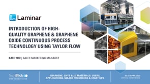
New effective but proven technology for Graphene and Graphene Oxide! The Taylor Reactor, utilizing the transit flow area between Laminar and Turbulence called ‘Taylor Flow’ can overcome the current challenges during the development and mass production. The presentation will show the advantages with the various publications 1) Reaction time reduction while getting high yield 2) High quality 3) Tailored size and 4) Easy scale up.
- R2R Printed Carbon Nanotube TFT Sheets
Speaker: Patrick Malenfant | Company: National Research Council Canada (NRCC) | Date: 10-11 March 2021 | Full Presentation This presentation covers our progress in high purity semiconducting single-walled carbon nanotube (sc-SWCNT) enrichment and transistor fabrication via solution based processes. I will highlight our recent progress in understanding sc-SWCNT enrichment using conjugated polymers (isolation of high purity sc-SWCNT), with special consideration given to the effects of solvent parameters and doping on the yield/purity of the final product. Fully printed transistors combining R2R gravure and inkjet-printing will be described as well as our recent progress in realizing “limitless” R2R gravure printed TFT backplanes capable of driving an e-paper display. Patrick R. L. Malenfant*(1), Jianfu Ding(1), Jianying Ouyang(1), Zhao Li(1), Chang Guo(1), Jacques Lefebvre(1), Paul Finnie(1), Francois Lapointe(1), Gyoujin Cho(2) (1)National Research Council Canada, 1200 Montreal Road, Ottawa, ON, K1A 0R6, Canada. (2)Dept. of Biophysics, Sungkyunkwan University (SKKU), South Korea Patrick Malenfant Director of Research Development @ National Research Council Canada (NRCC) Bio Dr. Patrick Malenfant studied chemistry at the University of Ottawa (BSc 1995), Cornell University (MSc 1997), and the University of California - Berkeley (PhD 2000). He has 10 years of industrial R&D experience including a one year postdoc at IBM's TJ Watson Research Center and 9 years at the GE Global Research Center where he developed nanomaterials for Aerospace, Healthcare, and Organic Electronics applications. He joined the National Research Council of Canada in 2010 as a Senior Research Officer. He is currently the Director of R&D in the Security and Disruptive Technologies Research Center overseeing activities in Quantum Science, Printed Electronics and Structural Materials. Join TechBlick on an annual pass to join all live online conference or online version of onsite conference access library of on-demand talks (600 talks + PDFs) portfolio of expert led masterclass year-round platform https://www.techblick.com/ And do NOT miss our flagship event in Berlin on 17-18 OCT 2023 focused on Reshaping the Future of Electronics. This event attracts 550-600 participants from all the world and offers a superb ambience and dynamic exhibition floor. To learn more visit https://www.techblick.com/electronicsreshaped To see feedback about previous event see https://www.techblick.com/events-agenda
- Commercial Ready High Energy Density Ultra-Fast Charge Cells
Speaker: Benjamin Park | Company: Enevate Corporation | Date: 9-10 Feb 2022 | Full Presentation Why bother with fast charge for EV batteries? Charge rate goes beyond driver convenience - it addresses core EV adoption issues such as addressing the fact that only 20% of cars have access to overnight charging, fast charging helps improve existing infrastructure utilization, and it supports drivers becoming more comfortable with less expensive vehicles that have shorter range lowering the price for those vehicles. Enevate is a battery technology company supplying breakthrough Extreme Fast Charge Technology with its pure silicon-dominant cells that are solving these crucial EV adoption issues. Join TechBlick on an annual pass to join all live online conference or online version of onsite conference access library of on-demand talks (600 talks + PDFs) portfolio of expert led masterclass year-round platform https://www.techblick.com/ Our next battery-related event will take place on 15-16 FEB 2023, covering 1) Solid-State Batteries: Innovations, Promising Start-Ups, & Future Roadmap 2) Battery Materials: Next-Generation & Beyond Lithium Ion The speakers include: General Motors, Graphenix Development, Brookhaven National Laboratory, Fraunhofer IKTS, RWTH Aachen University, Lawrence Livermore National Laboratories, Meta Materials Inc, Skeleton Technologies, Solid State Battery Inc, Argonne National Laboratories, OneD Battery Sciences, VTT, Leyden Jar Technologies B.V., b-Science, Rho Motion, Wevo-Chemie, LiNA Energy, CNM Technologies, Ionblox, Empa, Zinc8 Energy Solutions, Avicenne Energy, Echiontech, South8 Technologies, Basquevolt, NanoXplore, Chasm, Li Metal, Sila Nanotechnologies, Quantumscape (tentative), Fraunhofer ISI, etc https://www.techblick.com/
- Flexible thin-film loudspeaker
MIT engineers have developed a paper-thin loudspeaker that can turn any surface into an active audio source. This thin-film loudspeaker produces sound with minimal distortion while using a fraction of the energy required by a traditional loudspeaker. The hand-sized loudspeaker the team demonstrated, which weighs about as much as a dime, can generate high-quality sound no matter what surface the film is bonded to. To achieve these properties, the researchers pioneered a deceptively simple fabrication technique, which requires only three basic steps and can be scaled up to produce ultrathin loudspeakers large enough to cover the inside of an automobile or to wallpaper a room. Used this way, the thin-film loudspeaker could provide active noise cancellation in clamorous environments, such as an airplane cockpit, by generating the sound of the same amplitude but opposite phase; the two sounds cancel each other out. The flexible device could also be used for immersive entertainment, perhaps by providing three-dimensional audio in a theater or theme park ride. And because it is lightweight and requires such a small amount of power to operate, the device is well-suited for applications on smart devices where battery life is limited. “It feels remarkable to take what looks like a slender sheet of paper, attach two clips to it, plug it into the headphone port of your computer, and start hearing sounds emanating from it. It can be used anywhere. One just needs a smidgeon of electrical power to run it,” says Vladimir Bulović, the Fariborz Maseeh Chair in Emerging Technology, leader of the Organic and Nanostructured Electronics Laboratory (ONE Lab), director of MIT.nano, and senior author of the paper. Bulović wrote the paper with lead author Jinchi Han, a ONE Lab postdoc, and co-senior author Jeffrey Lang, the Vitesse Professor of Electrical Engineering. The research is published today in IEEE Transactions of Industrial Electronics. A new approach A typical loudspeaker found in headphones or an audio system uses electric current inputs that pass through a coil of wire that generates a magnetic field, which moves a speaker membrane, that moves the air above it, that makes the sound we hear. By contrast, the new loudspeaker simplifies the speaker design by using a thin film of a shaped piezoelectric material that moves when voltage is applied over it, which moves the air above it and generates sound. Most thin-film loudspeakers are designed to be freestanding because the film must bend freely to produce sound. Mounting these loudspeakers onto a surface would impede the vibration and hamper their ability to generate sound. To overcome this problem, the MIT team rethought the design of a thin-film loudspeaker. Rather than having the entire material vibrate, their design relies on tiny domes on a thin layer of piezoelectric material which each vibrate individually. These domes, each only a few hair widths across, are surrounded by spacer layers on the top and bottom of the film that protect them from the mounting surface while still enabling them to vibrate freely. The same spacer layers protect the domes from abrasion and impact during day-to-day handling, enhancing the loudspeaker’s durability. To build the loudspeaker, the researchers used a laser to cut tiny holes into a thin sheet of PET, which is a type of lightweight plastic. They laminated the underside of that perforated PET layer with a very thin film (as thin as 8 microns) of piezoelectric material, called PVDF. Then they applied a vacuum above the bonded sheets and a heat source, at 80 degrees Celsius, underneath them. Because the PVDF layer is so thin, the pressure difference created by the vacuum and heat source caused it to bulge. The PVDF can’t force its way through the PET layer, so tiny domes protrude in areas where they aren’t blocked by PET. These protrusions self-align with the holes in the PET layer. The researchers then laminate the other side of the PVDF with another PET layer to act as a spacer between the domes and the bonding surface. “This is a very simple, straightforward process. It would allow us to produce these loudspeakers in a high-throughput fashion if we integrate it with a roll-to-roll process in the future. That means it could be fabricated in large amounts, like wallpaper to cover walls, cars, or aircraft interiors,” Han says. High quality, low power The domes are 15 microns in height, about one-sixth the thickness of a human hair, and they only move up and down about half a micron when they vibrate. Each dome is a single sound-generation unit, so it takes thousands of these tiny domes vibrating together to produce audible sound. An added benefit of the team’s simple fabrication process is its tunability — the researchers can change the size of the holes in the PET to control the size of the domes. Domes with a larger radius displace more air and produce more sound, but larger domes also have lower resonance frequency. The resonance frequency is the frequency at which the device operates most efficiently, and a lower resonance frequency leads to audio distortion. Once the researchers perfected the fabrication technique, they tested several different dome sizes and piezoelectric layer thicknesses to arrive at an optimal combination. They tested their thin-film loudspeaker by mounting it to a wall 30 centimeters from a microphone to measure the sound pressure level, recorded in decibels. When 25 volts of electricity were passed through the device at 1 kilohertz (a rate of 1,000 cycles per second), the speaker produced high-quality sound at conversational levels of 66 decibels. At 10 kilohertz, the sound pressure level increased to 86 decibels, about the same volume level as city traffic. The energy-efficient device only requires about 100 milliwatts of power per square meter of speaker area. By contrast, an average home speaker might consume more than 1 watt of power to generate similar sound pressure at a comparable distance. Because the tiny domes are vibrating, rather than the entire film, the loudspeaker has a high enough resonance frequency that it can be used effectively for ultrasound applications, like imaging, Han explains. Ultrasound imaging uses very high-frequency sound waves to produce images, and higher frequencies yield better image resolution. The device could also use ultrasound to detect where a human is standing in a room, just like bats do use echolocation, and then shape the sound waves to follow the person as they move, Bulović says. If the vibrating domes of the thin film are covered with a reflective surface, they could be used to create patterns of light for future display technologies. If immersed in a liquid, the vibrating membranes could provide a novel method of stirring chemicals, enabling chemical processing techniques that could use less energy than large batch processing methods. “We have the ability to precisely generate mechanical motion of air by activating a physical surface that is scalable. The options of how to use this technology are limitless,” Bulović says. “I think this is a very creative approach to making this class of ultra-thin speakers,” says Ioannis (John) Kymissis, Kenneth Brayer Professor of Electrical Engineering and Chair of the Department of Electrical Engineering at Columbia University, who was not involved with this research. “The strategy of doming the film stack using photolithographically patterned templates is quite unique and likely to lead to a range of new applications in speakers and microphones.” This work is funded, in part, by the research grant from the Ford Motor Company and a gift from Lendlease, Inc. For more information, visit: https://news.mit.edu/2022/low-power-thin-loudspeaker-0426