


29 September 2022
Monolithic chip-scale integration of QD color converters with GaN microLED chips
Manufacturing in particular mass transfer and repair remain the biggest challenges in realization of microLED displays. To simplify the process, many propose to transfer only the blue (or even a UV) LED and achieve RGB by depositing color converters such as quantum dots. This requires an additional deposition step. But what if one could achieve chip-scale monolithic integration of QDs and GaN microLED chips? Indeed, Saphlux proposes just this and will present this on 30Nov-1Dec 2022 at TechBlick's microLED and QD event www.TechBlick.com/microLEDs Saphlux has taken this approach one step further. Instead of post-transfer deposition of QDs, their technology enables chip-scale integration of quantum dots and microLEDs. In this technique, a nano-porous structure is directly formed inside LEDs to serve as a natural vessel for in-situ QD integration. The effective light path can be extended by nano-porous structure to boost the overall efficiency due to the strong scattering effect. The reliability of quantum dots is - it is claimed- also improved greatly because of the high thermal conductivity of gallium nitride material. Importantly, this technology claims to be able to integrate red, green, and blue pixels monolithically into a single chip to greatly reduce the complexity and cost of Micro-LED display manufacturing.
In this technique, nanopores in LEDs can be created by dipping the material in an acidic solution and applying a bias voltage, which drives electro-chemical etch...

26 September 2022
Active Mold Packaging – Additive IC Packaging For mmWave Applications
Speaker: Florian Roick | Company: LPKF | Date: 10-11 March 2021 | Full Presentation This presentation investigates the capabilities of Active Mold Packaging towards mmWave application. First the dielectric properties of three different AMP-EMCs are measured in the D-band. Second, the reflection coefficient S11, as well as the H- and E-plane radiation patterns are determined for a set of AMP manufactured 60 GHz bow-tie slot and dual dipole antennas. Where the measured results are compared to the design values and differences are discussed. And third, the D-band EMI shielding effectiveness of the electroless plated Cu/Ni/Au layer on the surface of three different AMP-EMCs is measured. Florian Roick Business Development Manager Active Mold Packaging @ LPKF Bio M. Sc. Florian Roick, Business Development Manager Active Mold Packaging. Born in 1981. He holds a degree as Bachelor of Science in Applied Physics from Dublin Institute of Technology. And a degree as Master of Science in Electrical Engineering with focus on laser systems, laser physics and microsystems engineering from Hochschule Bremen. Since 2006 employed at LPKF Laser & Electronics AG, until 2008 as application engineer for the StencilLaser business unit. Between 2008 and 2019 strategic product manager responsible for aligning the product portfolio with the needs and requirements of the PCB and SMT markets. Since 2019 Business Development Manager for LPKF’s Active Mold Packaging technology. That is to electrically fun...

19 September 2022
Technical & Styling Approaches For Intelligent Surface Illumination
Speaker: Mathias Rönnfeldt | Company: Lightworks | Date: 10-11 March 2021 | Full Presentation Current light system development is much more than the sum of the right light source, the material setup and light output. Together with our customers Lightworks GmbH is creating more and more user-oriented lighting experiences. Main focus is the seamless combination of innovative lighting technologies like IMSE as well as advanced surfaces, materials and processes out of our network. This approach allows maximum design freedom during concept and series development for our customers and their clients. Join TechBlick on an annual pass to join all live online conference or online version of onsite conference access library of on-demand talks (600 talks + PDFs) portfolio of expert led masterclass year-round platform https://www.techblick.com/ And do NOT miss our flagship event in Berlin on 17-18 OCT 2023 focused on Reshaping the Future of Electronics. This event attracts 550-600 participants from all the world and offers a superb ambience and dynamic exhibition floor. To learn more visit https://www.techblick.com/electronicsreshaped To see feedback about previous event see https://www.techblick.com/events-agenda...

18 September 2022
Mass Transfer of uLEDs:Overcoming dimensional/manufacturing variations with magnetic head/stamp tec
microLED display technology requires massive parallel transfer technology. This is a complex technology as it is and will grow even more complex as displays with smaller dies and high PPIs are considered. This has been one of the frontiers of development in the uLED industry. Many parallel transfer approaches have been proposed. Most are based on a type of stamp which picks up the microLED dies from the growth substrate and transfers them onto the target substrates, placing them at the right spot. A critical challenge is how to overcome inevitable height and dimensional variations of uLEDs using standard elastomer-based microLED technology, which, if not managed properly, can adversely impact that all-important figure-of-merit: yield! LuxNour Technologies Inc. is proposing a novel approach based on electromagnetic stamps which can - as shown in slide 1- tolerate tens of σ in uLED variation! This increases yield and eases the pressure on exact control of the microLED dimensions during the growth. Join the specialist TechBlick conference on microLEDs on 30-Nov and 1-Dec to learn morewww.TechBlick.com/microLEDs Makarem Hussein in slide one shows the structure of such an electromagnetic head, containing a bulk electromagnetic at the back, a non-magnetic dielectric element in between, and a pattern of high permeability materials (e.g., Ni) and openings. The high permeability areas shield the bulk magnetic, preventing its flux from protruding out. In contrast, the openings repres...

29 September 2022
MicroLEDs, printed electronics and laser printing?
Holst has developed and advanced the so-called LIFT technology to enable even the laser transfer or laser printing of microcomponents such as microLEDs with high 1-um precision. In the first slide you can see a comparison of the classical Laser Induced Forward Transfer (LIFT) vs the technique developed at Holst which is Volume-Controlled Laser Printing (VCLP).
In LIFT, the laser illumination causes a jetting of low to medium viscosity inks onto the acceptor or target substrate. This is not a young technology and some consider it the digitization of screen printing. In the example here you can see 200um dots of conductive paste printed with the LIFT process.
The VCLP is different. Here, the laser releases fine droplets onto the target/acceptor substrate. Given the volume control, better resolution is accessible. The example herein shows 40um dots of highly viscous solder paste printed using VCLP technology. Note that here the high-throughput deposition of ultrafine interconnects, such as conductive adhesives and solder pastes, is from a structured carrier plate covered with a proprietary permanent release coating
An important feature of the VCLP technique is the control of heat flux. Without this the laser printing can result in blurred or poor definition. To manage the heat flux, Holst has developed a proprietary “permanent” stack for clean, fine interconnect printing. In the second slide, you can see the positive impact of this layer in achieving well defined high reso...

23 September 2022
What is the future market for microLEDs in terms of unit sales, application, chip type, backplane?
The slides below share some key forecasts and analysits by Jerry Kang from Omdia - one of the leading analysts in the field - who will present live online at TechBlick's microLED and QD event on 30Nov-1Dec www.TechBlick.com/microLEDs Slide 1 shows that the microLED market will experience substantial growth in the coming years. In 2021, the sales were expected to be just 0.12k units, reflecting the lack of technology maturity and the manufacturing high cost/low yield. In 2029, the figure is expected to reach 12.7M units per area. This is a transformational growth, and yet still represents just 0.3% of the total FPD market! Slide 1 also shows the split of the market - in thousands of units - by application. The first to arrive were public displays owing to low technical barriers and much larger dies as well as ultra low PPI. Premium TV have also arrived and will grow. Here, the superior performance of color gamut, luminance, and contrast delivers value. Smart watches will be a drive of unit sales, as here the small size and lower PPI translate to lower technical barriers. Slide 2 shows the evolution of the market by backplane technology. MicroLED on Silicon (on CMOS) is suited to high PPI AR or HUD devices. LTPS backplane is ideal for small and medium sized applications like smart watches due to high mobility of LTPS but LTPS does not scale to large areas due to non-uniformity of p-Si. Oxide TFTs can be scaled to Gen8 whilst PCBs will be used for ultra large displays such as ...
18 September 2022
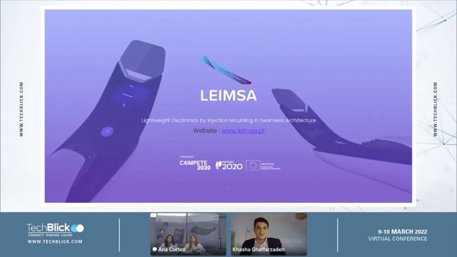
LEIMSA – Lightweight Electronics by Injection Moulding in Seamless Architecture
LEIMSA is an ambitious 5M Euro project bringing together many of the key players across the value chain to create structural electronics using the integration of IMD (in-mold decoration), IML (in-mold labling), IME (in-mold electronics), HPF (high pressure forming, etc). The project partners include Simoldes Plastics Celoplás, Plásticos para a Indústria, S.A. DTx - Digital Transformation CoLAB Bosch. The project partners include Elantas Proell Covestro DuPont Hofmann Biebling Covestro Sabic Kurz Grewus, etc The final demonstrator will seemlessly integrate into a 3D console a transparent display, a capacitive display, a slider (capacitive | backlighted), touch buttons with RGB LEDS and haptic feedback, small display etc. In the video below Sandra Melo and Ana Cortez explain the parts that are being integrated using into the console...

18 September 2022
QD-Si Image Sensors- beating InGaAs and SiGe in the NIR and SWIR regions with 1.62-2.2um pixel pitch
It took roughly 20 years of R&D to commercialize colloidal quantum dots (CQD) image sensors, which are the first commercial products in the marketplace to use CQDs in electro-active devices in contrast to all of the other current products that use CQDs in photoluminescence mode. First, why quantum dots? The particle size of PbS QDs can be tuned to absorb thoughout the SWIR region spanning from 1000nm to 2500nm. This is shown in slide below, showing also that these QDs can also absorb in the NIR, visible, and UV regions at the same time. Second, why quantum dots + silicon? Obviously the most advanced imaging technology is based on silicon. However, silicon is not sensitive to NIR and SWIR. As such, InGaAs and SiGe sensors have taken hold of this market. However, they are often expensive and their heterogenous integration with silicon read-out circuity (ROIC) can add to complexity and limit pixel sizes/pitches although advances in Cu-Cu bonding may change this. As shown in the slide below, The QDs can be spin coated atop a 300mm silicon wafer. Single PbS QDs are formed into thin QD films with a ligand matrix. Out of this, a QF (quantum film) photodiode if formed with top and bottom electrodes (which must be transparent to a broad light spectrum). These QD photodiodes are formed atop the BEOL of a top-side illuminated image sensor. Cu vias are then used to connect the QD layer to the image sensor. In addition to bringing silicon image sensor technology to the NIR/SWIR spectrum...