Search Results
Search this site
1075 results found with an empty search
- Innovation in Luminous and HMI Surfaces
This video looks at the latest innovations in luminous and HMI (human-machine interface) surfaces. Forvia is a tier one automotive company with 150,000 employees and 300 sites worldwide, aiming to become one of the world's largest automotive technology companies. Their innovation team, located in Scotland, focuses on display and HMI product lines, advanced backlight design, and other next-generation solutions. Forvia's ecosystem of startups that have been acquired focuses on developing the next generation of printed electronics. Forvia's projects include working with car manufacturers on exterior lighting with large continuous limited surfaces and pixelation. They are developing large area dynamic lighting with functionality as well as decoration across the IP door panels and even into the roof liner. For the front of the car, they are working on grill elimination and brand lighting, combining backlighting technologies and low-resolution displays. However, their main focus is on the cockpit display. The cockpit display is a large 3D glass panel with screens and other electronic functionalities bonded behind it. Forvia takes standard industry screens and combines them with lighting and other functionalities to create the perception of very large information surfaces while reducing costs. Forvia's light tile technology uses LEDs, printed electronics, and beta inside transparent polymers with optics around them to create homogenous lighting and backlighting of surfaces. By putting the LEDs behind automotive materials and replacing them with Dynamic rgbs. Forvia delivers a dynamic backlighting light with a thin package, providing more space for passengers. By backlighting a range of interesting materials, Forvia achieves a dynamic effect with a small number of LEDs, delivering this dynamic capability at a lower cost and power consumption. They can integrate other functionalities like capacitive switching into the same electrical circuit. Forvia's advancements in luminous and HMI surfaces provide exciting possibilities for the automotive industry. By combining different technologies, they are creating innovative and dynamic lighting and display solutions that improve user experience while reducing costs and power consumption. Hear more talks like this at TechBick's The Future of Electronics RESHAPED conference and exhibition in Berlin on 17 & 18 October, 2023 - see www.TechBlick.com
- Pioneering Printed Electronics with Advanced 3D Printing Technology
Introduction: The rapidly evolving electronics industry demands innovative solutions for quick prototyping and the creation of uniquely shaped devices. An advanced 3D printer, specifically designed for printed electronics, has the potential to revolutionize the sector. In this blog post, we will delve into the key features and capabilities of this groundbreaking 3D printing technology, its applications, and its potential impact on the electronics industry. A Comprehensive 3D Printing Solution for Electronics: The cutting-edge 3D printer in focus offers three essential functions: resin printing, circuit formation, and part mounting. This all-in-one machine can produce printed circuit boards (PCBs) within a day using an additive process, eliminating the need for traditional glass and metal mask tools. This allows users to manufacture even a single piece, making it an ideal choice for rapid prototyping and production of uniquely shaped devices. Innovative Applications and Use Cases: The 3D printer's versatility and potential in the electronics industry have already been demonstrated in various applications. Two of the primary use cases for this advanced technology include: Rapid Prototyping: The 3D printer can manufacture multiple boards simultaneously, reducing the overall production time. The latest iteration of this technology is designed to produce boards in just 16 hours, making it an excellent tool for super rapid prototyping. Unique Shaped Devices: The printer's ability to print resin and form multilayer circuits enables it to create devices with complex structures and shapes. This is particularly useful for designers and engineers looking to create innovative products that require unconventional form factors. State-of-the-Art Materials and Processes: This 3D printer employs low-temperature processes and cutting-edge materials to achieve high-quality, smooth circuitry. In collaboration with chemical suppliers, researchers have developed unique materials with excellent durability, high-temperature resistance, and electrical properties. The low-temperature sintering process used in the printer allows for the production of circuits with smooth surfaces and tight tolerances The proponents of this 3D printing technology believe that additive electronics can have a profound impact on the industry by minimizing waste, reducing transportation energy, accelerating innovation, and contributing to global engineering equality. With this advanced 3D printer, the goal is to revolutionize the printed electronics sector, paving the way for more efficient and eco-friendly manufacturing processes. The advanced 3D printer for electronics is an innovative and versatile solution, offering rapid prototyping and the ability to create uniquely shaped devices. By leveraging state-of-the-art materials and processes, this technology delivers high-quality, smooth circuitry in a short timeframe. The commitment to minimizing waste and fostering innovation makes this 3D printing technology a promising development for the future of the electronics industry. Keywords: advanced 3D printer, printed electronics, rapid prototyping, unique shaped devices, low-temperature processes, additive electronics
- BEYOLEX™ for Soft Circuit Solutions (Panasonic)
Author: Tsuyoshi Takeda, Panasonic The Electronic Materials Business Division of Panasonic Industry Co.,Ltd. (Panasonic) is a premier supplier of electronic materials like printed circuit boards laminates, semiconductor packaging materials, display films and other leading-edge products. Leveraging our core expertise in high-performance thermosetting polymer chemistry, we developed BEYOLEX™, a fully cross-linked, non-silicone, thermosetting stretchable film. BEYOLEX™ is specifically designed as a soft, stretchable, and durable substrate for reliable printed electronics. BEYOLEX™ exhibits superior performance when compared to existing stretchable films like Thermoplastic Polyurethane (TPU) and Polydimethylsiloxane (PDMS) and is under evaluation and qualification for a wide variety of demanding applications. In collaboration with our innovative partners, Panasonic introduces our latest case studies on soft circuit development which is one of the promising applications of BEYOLEX™. Case Study 1: Pliable PCB made with copper sintering ink InnovationLab and Panasonic developed a pliable PCB demonstrator. This device was designed and manufactured by InnovationLab using BEYOLEX™ and sintered copper ink. Generally, the copper inks require a high sintering temperature (>160 °C), which is extremely challenging for TPU. As can be seen in Pic 1, the BEYOLEX™ substrate had no difficulty tolerating the sintering temperature and exhibited no damage from the process. Furthermore, the combination of the high temperature tolerance of BEYOLEX™ and the solderability of the sintered copper ink enabled component mounting with standard solders such as Sn-Bi or SAC305: resulting in reliable and high density assemblies and delivering a functional PCB with more pliability and softness than typical flexible printed circuits (FPCs.) Pic 1: Pliable PCB made by InnovationLab Case Study 2: Stretchable hybrid PCB made using copper ink and stretchable silver paste Kelenn Technology, a leading manufacturer of printing equipment, also makes functional inks that are customized for their printing systems. Using their proprietary Direct Material Deposition (DMD) technology, Kelenn Technology printed land pads with copper ink and circuit traces with stretchable silver-based paste onto BEYOLEX™ film (Pic 2). This hybrid circuit produced a solderable, stretchable PCB configuration that would be difficult to achieve with copper circuitry alone. Definitely, BEYOLEX™ is the only substrate solution for this design. Pic 2: Stretchable PCB made by Kelenn Technology Subsequently, Panasonic engineers reflowed solder paste onto test vehicles prepared by Kelenn Technology. We printed an industry standard SAC305 solder paste and reflowed the part in a Vapor Solder Oven with a temperature of 230°C. We confirmed both the solderability of the copper ink pads provided by Kelenn Technology as well as the mechanical integrity of BEYOLEX™ after soldering (Pic 3). As a result of this test, we believe BEYOLEX™, with sintered copper ink, is a promising solution for solderable, pliable or even stretchable PCB constructions. Pic 3: Soldering on Cu Case study 3: Tackling the challenges of truly stretchable electronics Stretchable silver pastes are an attractive conductor solution for new form factor devices. However, these polymer composite pastes have inherent limitations for forming truly stretchable electronics; typically, the resistance increases significantly with each elongation cycle and these increases are cumulative, climbing with each stretch cycle. A printable Liquid Metal Based Composite developed by University of Coimbra (UoC) is a promising solution to this issue. UoC’s ink exhibits metallic conductivity and much lower resistance change during stretch cycles compared to silver-polymer pastes. Thanks to the lack of plastic deformation of BEYOLEX™, UoC’s ink printed on BEYOLEX™ looks to be a promising combination for truly stretchable electronics requiring repeated stretching (Pic 4). Pic 4: Stretchable LED with capacitive touch by UoC The soft-circuit solutions made with BEYOLEX™ introduced in this article are made by additive printing processes which are generally more environmentally friendly than the conventional subtractive PCB fabrication process. Panasonic’s Electronic Materials Business Division keeps contributing to create value and to society through innovative materials. To learn more about BEYOLEX™, please visit https://industry.panasonic.eu/products/devices/electronic-materials/beyolextm-thermosetting-stretchable-film
- 🩺Advanced screen printing for medical sensors
Marco Galazio discussed advanced screen printing techniques for manufacturing medical sensors, specifically focusing on continuous glucose monitoring (CGM) sensors. Applied Materials, the parent company, has a long history in the semiconductor business and has diversified into adjacent markets, including medical sensors. Their objective is to miniaturize the sensor's components and optimize the screen printing process for various layers in the sensor. The screen printing process involves multiple steps and layers, such as the circuit layer with nano silver-based paste, the carbon sensing element, the insulating resist layer, and the silver/silver chloride material layer. Each layer requires optimization of printing speed, force, and curing conditions to achieve the desired specifications. For instance, the nano silver-based paste allows for features around 50 microns and requires careful management of the printing speed to balance shorting risks and process efficiency. By benchmarking against other mainstream applications, they found that screen printing could be more cost-effective and competitive. The manufacturing tool they use integrates various subsystems, such as automation, inspection, and process control, for a fully packaged solution. Although the glucose-sensitive layer isn't integrated into the presented process, it is added later to create the complete biosensor. Challenges remain in using nanosilver for miniaturization, but improvements are ongoing.
- 🌱 Making Print Electronics Sustainable: Insights from Coatema 🌍
1️⃣ Tackling waste: Focusing on sustainable materials to reduce waste and improve recyclability. 2️⃣ Exploring new materials: Nanocellulose for biodegradable printed electronics devices. 3️⃣ Innovative processes: Thermal nanoimprint lithography for functional surfaces without additional materials. 4️⃣ Enhanced functionality: Smart devices that improve the sustainability of packaged goods. 5️⃣ Working together: Collaboration with partners to ensure end-to-end sustainability in the printed electronics industry. #SustainableTech #PrintedElectronics #GreenInnovation #Sustainable Electronics Thomas Exlager, a process engineer at Coatema, discussed making printed electronics more sustainable by focusing on the waste problem. He presented four solutions to this issue: 1) choosing materials wisely, as exemplified by the Flex Function to Sustain project, which developed a mono-material system for Capri-Sun packaging; 2) using new materials like nanocellulose for printed biosensors in the Green Sense project; 3) adopting new process technology, such as thermal nanoimprint lithography, to create functional surfaces without additional materials; and 4) developing smart devices or materials to improve sustainability. Thomas emphasized that, while Coatema is not responsible for the sustainability aspects of these projects, the company can provide knowledge and work as an intermediary between partners.
- Designing Conductive Inks for the Market: Bio & eHealth
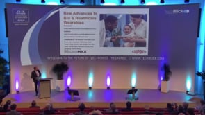
Celanesae Micromax | presested live onsite in Eindhoven in OCT 2022 This is an AI-generated summary of the talk There are a lot of different applications for biosensors, such as blood glucose measurement, drug delivery, DNA testing, food and beverage testing, and environmental sensors. I think the list can be extended to include blood gas detection or measuring urine detection. Blood glucose test strips are used to measure blood glucose levels. The next generation is the continuous glucose monitoring patch, which doesn't require you to take a drop of blood many times over the day. The principle is the same as a blood glucose test strip, but the needle goes in the skin not so deep, but going into the skin, and it measures the diffused glucose in the interstellar fluid in the skin. The electrocardiogram is a simple description of a muscle contraction. It is used in wellness applications as well as medical applications, and therefore the material must really constant and that starts to be really challenging. I think the principle is always the same, and you can measure an electrical impulse in many parts of the body. The design of an ECG electrode is that you have a single disposable patch, and typically use silver, silver chloride electrodes. However, the gel can cause skin irritation, and the patch is limited in the shelf life or the usable time. We are not only focused on ECG and blood glucose, we are also working on other products. The key word is partnership, and the more information we have, the better it is for us to create and design products for it. Partnership from the beginning, understanding what is needed and first the application itself, and then the manufacturing conditions which are typically more more familiar with us, is an important step or thing. The latest developments at the moment and where we are working on include improving pay, stability, longer screen life and so on. Here is a list of different solvents, and we concentrate very often on thf because if a paste is resistant to thf it covers most of the other solvents which could be there. And now I give you an impression what we are doing. We are improving our products and formulating new products, and a new tendency is going to more cross-linked formulations. These inks dry at lower temperatures, and can be used on other substrates. The cross-linking is done after printing, drying, and taking it off the pet. It gives a better adhesion and resistance against mechanical stress, and on one hand it's more acid and solvent and whatever resistant We are developing pastes for the blood glucose and ag market, and the newest one is some cross-linked compositions for more abrasion resistance, hydrogel stability or other solvents. For biosensor business, it's really difficult to say. It's depending how many iterative steps you need, and if you're talking about medical applications, where really everything must work under every condition and you must be absolutely safe, or if you are more in the wellness area.
- Critical to Performance Metrics of Functional Materials for IME
Speaker: Erika Rebrosova | Company: Sun Chemical | Date: 24-Jun-22 | Full Presentation 🚀 In-mold electronics (IME) are gaining attention for their promise of thinner and lighter weight parts, and less complex assembly processes. 🔬 Advances in 3D formable and injection moldable electronic materials are enabling IME applications to emerge. 💼 Multiple user cases have demonstrated the applicability of IME for automotive interiors, appliances, consumer electronics, industrial controls, deicing lenses, heaters and more. 🌞 Sun Chemical has leveraged its long-time expertise in in-mold decoration ink technologies to develop best-in-class in-mold electronic inks. 💡 Check-out the presentation below by Erika to learn more. #inmold #electronics #innovation #manufacturing #trends #technology #sunchemical
- Key highlights of talk given by DTI at TechBlick in summer 2022 on copper inks
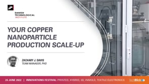
This summary is fully AI-generated based on the presentation 👉 We have several different types of reactors at our disposal for making and building nanomaterials, some of which can produce up to 80 liters of material per batch. Our reactors are PLC automated and have monitoring for quality control. 👉 Some of the materials we've worked with include platinum alloys, silver nanoparticles, copper nanoparticles, copper and silver nanowires, ferrite, high dielectric materials, and even graphene. 👉 We have been able to validate up to ten kilos per day of nano copper production, with a current production cost of around €300 per kilo. Our goal is to go at least below €100 per kilo, making these materials much more cost-effective than existing conductive inks. 👉 We have made an inkjet formulation for conductive inks, with photonic sintering that can produce a half-micrometer thick layer with good conductivity. We are currently working on a screen-printable formulation aiming for a 50 million square foot print.
- Fine line screen printing - applications
This text is auto transcribed and auto-summarized by AI: Screen printing is becoming increasingly finer and smaller, and it is expected that within a few years we will be reaching 20 micrometer line widths and maybe even lower. The wafer per hour rate for the back end processes is also rising, and it is projected to rise to >10,000 wafers per hour by the next years The state of the art for screen printing on solar cells is 19 micrometers and above, with an aspect ratio of 1818 micrometers. This is a relatively easy application, because the pictures are very wide and interrupted lines can be tolerated. Micro-led displays are very hot display topic, and one of the key uniques of this display technology is that you can create bezel free displays. This means that you can create a larger display by putting together many kind of smaller tiles and building up the big display. One way to create wraparound edge electrodes is to drill via into the glass, fill the field and feel the field through glass fires. But this is really not elegant, so a more interesting approach would be to create this so called wraparound edge electrodes. Screen printing can produce very fine lines, but as micro led dyes shrink in size, the bond sizes and metallization lines will also get smaller, which means that if screen printing is to stay competitive in this technology, it also has to produce ever finer lines. Applied Materials showed how they can print screen printed lines as fine as 15 micrometers, but the application is very challenging because it cannot tolerate broken interrupted lines and must have defect-free metallization on 90% of the tiles. Samsung uses a PVD process developed by a Korean company, but if screen printing could produce fine lines, 15 micrometers or less without defects, maybe this could be with very little defect [ this is in our view too big challenge for screen printing] Another application that I wanted to highlight is around flexible hybrid electronics, and I think many of the technology hurdles that have held back this technology are being cleared away now. And I think screen printing could also play a role here. The wiring lines can be screen printed, but the pins of the ICs are much narrower than the wiring lines. So one needs to have a fan out structure connecting the pins to the actual wiring. Screen printing cannot do the wiring and the final structure just based on screen printing process, but if fine line screen printing would be further advanced, then this would be possible. This image is from Nexflex, and I took some of these images from a presentation by Komori in Japan. It shows a very interesting application for Transparent Touch or HMIs, where one maybe does not need a protective layer. The requirements for a transparent touch display are very different from the requirements for a transparent switch, so the line width needs to be a lot narrower. The line widths are generally sub four micrometers, and this shows you the requirement for this industry. If screen printing could print ever finer lines, then it would stay relevant in this application and be very competitive process, and the requirements have also shrunk over time. So if screen printing is to stay relevant, it needs to target sub 15 or so, maybe at least sub 20 micrometer range. Standard screen printing takes you down to 50-60 micrometers, but new screen printing technologies are taking you down to 20-15 micrometers [in lab conditions not production]. Then people start to use hybrid processes, such as screen printing plus laser plus photolithography. We want to focus on alternative technologies, so we talked about photovoltaic metallization, microgrid, flexible hybrid electronics, transparent light switches, edge electrodes, and LTCCs. Before going to the alternative technologies, I just want to mention maybe a couple of applications which I admitted in my presentation but are very important. In order to print very fine lines for 5G and LTCC, you need to have very good edge definition, so you need to be able to print lines as small as 15 micrometers In this hybrid screen printing process, the ink itself contains a photosensitive material, so you don't need a photoresist. This allows you to get very fine lines, and the ink is compatible with peat substrates. A hybrid screen printing process was developed by Kodak, where they created a metal mesh, and then used plating to thicken the layer and achieve bulk like bulk like conductivity. This process can go down to sub10 micrometers. A Japanese company can print complex patterns with just 1.5 micrometer line with silver nanoparticles, and they can cure the ink at low temperature. If you want to go below that level and achieve kind of one micrometer, then the reverse offset process is interesting. Reverse offset printing technique is very unique because you totally ink the roller mold, the ink semi absorbs into the mold material, and then the ink is transferred to the relief plate. This allows you to create metal meshes with just one micrometer line. Here's another, I think, interesting technology, by Asahi Kasei in Japan. This one uses a seamless roller mold, which is patterned not using just laser, but with electron beam lithography, and it produces very fine lines with very well defined edges and just 300 micrometers wide. Here you can see an application of printing aligned with a three micrometers for transparent RF ID on products without taking up real estate. There are a lot of hybrid and road roll technologies, and Panasonic has developed a process that allows them to print two micrometer lines with a good aspect ratio and a good sheet resistance of two ohms per square The main competition is photolithography, and Nippon Printing has achieved a line width of one micrometer in their products. This technology can be used for transparent displays, and the company is targeting the market of sub 40 inch displays. We looked at applications for screen printed lines, photovoltaic metallization, microgrids, transparent capacitive type switches, edge electrodes in capacitive touch displays, and hybrid and direct printing techniques.
- Advance printed electronics and standardization within the smart wearables industry
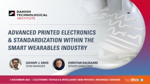
Speaker: Christian Dalsgaard | Company: Danish Technological Institute | Date: 2-Dec-22 | Full Presentation View the full video presentation here https://www.youtube.com/watch?v=V-TocfDHq5Y Recent years development of wearables evolves at the edge of the textile - and electronics industry with new demands for the supply chain. Printed electronics is a promising technology that bridges the gap between manufacturing cost, requests for advance vital sign monitoring and washability of most clothing. Endorsement of industry standards and technology capacities goes hand in hand to meet the demand for next generation wearables. In this talk, DTI’s speakers will present an outlook for printed electronics in this segment and demonstrate why e-textiles soon will play a significant role in healthcare, sport, and personal protective equipment. Join TechBlick on an annual pass to join all live online conference or online version of onsite conference access library of on-demand talks (600 talks + PDFs) portfolio of expert led masterclass year-round platform https://www.techblick.com/ And do NOT miss our flagship event in Berlin on 17-18 OCT 2023 focused on Reshaping the Future of Electronics. This event attracts 550-600 participants from all the world and offers a superb ambience and dynamic exhibition floor. To learn more visit https://www.techblick.com/electronicsreshaped To see feedback about previous event see https://www.techblick.com/events-agenda
- Advance printed electronics and standardization within the smart wearables industry
Speaker: Zachary James Davis | Company: Danish Technological Institute | Date: 2-Dec-22 | Full Presentation View the full video presentation here https://www.youtube.com/watch?v=V-TocfDHq5Y Recent years development of wearables evolves at the edge of the textile - and electronics industry with new demands for the supply chain. Printed electronics is a promising technology that bridges the gap between manufacturing cost, requests for advance vital sign monitoring and washability of most clothing. Endorsement of industry standards and technology capacities goes hand in hand to meet the demand for next generation wearables. In this talk, DTI’s speakers will present an outlook for printed electronics in this segment and demonstrate why e-textiles soon will play a significant role in healthcare, sport, and personal protective equipment. Join TechBlick on an annual pass to join all live online conference or online version of onsite conference access library of on-demand talks (600 talks + PDFs) portfolio of expert led masterclass year-round platform https://www.techblick.com/ And do NOT miss our flagship event in Berlin on 17-18 OCT 2023 focused on Reshaping the Future of Electronics. This event attracts 550-600 participants from all the world and offers a superb ambience and dynamic exhibition floor. To learn more visit https://www.techblick.com/electronicsreshaped To see feedback about previous event see https://www.techblick.com/events-agenda
- Connecting surfaces of the smart building to the cloud with sensors enabled through
printed electronics Speaker: Matt Johnson | Company: Laiier | Date: 12-13 October 2022 | Full Presentation Step into smart buildings of the future and you might not see a difference. Combining the scalability of coatings and building materials contemporary sensing techniques opens-up an incredible range of possibilities for predictive, preventative, and responsive maintenance. For Henkel, a global leader in specialized and cross-functional ink formulations for printed electronics, and Laiier a smart surface technology provider, the next decade will see the rise of smart buildings that integrate new capabilities into the built environment. Whether it’s office facilities that warn of leaking pipes, walls that heat our rooms, or floors that tell us when an elderly relative has suffered a fall, many of the core technologies are already here. Today, the challenge besides the technology innovation is more about building networks and creating markets. The presentation will cover the unique ecosystem required to bring this vision to life that includes the whole value chain from construction, materials, manufacturing industry to IoT integrators. The session will take the attendees through technical explanations and customer use cases demonstrating clear ROIs and customer insights. Join TechBlick on an annual pass to join all live online conference or online version of onsite conference access library of on-demand talks (600 talks + PDFs) portfolio of expert led masterclass year-round platform https://www.techblick.com/ And do NOT miss our flagship event in Berlin on 17-18 OCT 2023 focused on Reshaping the Future of Electronics. This event attracts 550-600 participants from all the world and offers a superb ambience and dynamic exhibition floor. To learn more visit https://www.techblick.com/electronicsreshaped To see feedback about previous event see https://www.techblick.com/events-agenda