Search Results
Search this site
1075 results found with an empty search
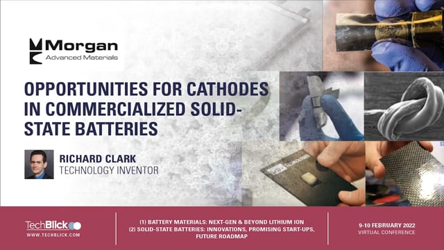
- Opportunities for cathodes in commercialized solid-state batteries
Speaker: Richard Clack | Company: Morgan Advanced Materials | Date: 9-10 Feb 2022 | Full Presentation As vast investment continues to pour into the solid-state battery development arena, many automotive OEM’s are projecting Start of Production within the next five years. Although there is no clear winner for the solid-state electrolyte, room temperature lithium-ion conductivity comparable with that of the liquid carbonate incumbent has been demonstrated at the laboratory and pilot plant scales. There are multiple options for the anode, ranging from thin lithium metal to “anode-less” in-situ generation to carbon-free high-loading silicon. Most work on the cathode has been focused on supply for current lithium-ion battery configurations, without recognizing the huge opportunity the move to solid-state provides, enabling lithium-free and high voltage options as well as the possibility of step-change reductions in cost. This talk will provide an overview of current developments in cathodes and project likely winners as solid-state batteries near commercialization. Join TechBlick on an annual pass to join all live online conference or online version of onsite conference access library of on-demand talks (600 talks + PDFs) portfolio of expert led masterclass year-round platform https://www.techblick.com/ Our next battery-related event will take place on 15-16 FEB 2023, covering 1) Solid-State Batteries: Innovations, Promising Start-Ups, & Future Roadmap 2) Battery Materials: Next-Generation & Beyond Lithium Ion The speakers include: General Motors, Graphenix Development, Brookhaven National Laboratory, Fraunhofer IKTS, RWTH Aachen University, Lawrence Livermore National Laboratories, Meta Materials Inc, Skeleton Technologies, Solid State Battery Inc, Argonne National Laboratories, OneD Battery Sciences, VTT, Leyden Jar Technologies B.V., b-Science, Rho Motion, Wevo-Chemie, LiNA Energy, CNM Technologies, Ionblox, Empa, Zinc8 Energy Solutions, Avicenne Energy, Echiontech, South8 Technologies, Basquevolt, NanoXplore, Chasm, Li Metal, Sila Nanotechnologies, Quantumscape (tentative), Fraunhofer ISI, etc https://www.techblick.com/ You can also check-out the agenda for our 2022 event here
- Murata- MXenes for electronics and printed electronics
An emerging class of two-dimensional (2-D) materials group, crystalline 2-D transition metal carbides or nitrides (MXene), has attracted considerable interest in the past decade. Murata has focused on an electrically conductive MXenes, especially for Ti3C2Tx in spray-coated film state (18000 S/cm at 5 um thickness). The hydrophilic nanosheet with outstanding properties (conductivity, high surface area and versatile surface chemistry) is a promising candidate of materials for flexible electronics using an eco-friendly manufacturing process. Swelling behavior of MXene by moisture is a roadblock for its applications in electronics. The interlayer spacing of layered structure is increased as stored in 60C/85% RH, which causes the degradation in electrical properties and the following oxidative reaction to TiO2. Murata has developed the concept of guest accommodation via hydrogen bonding to block water diffusion and demonstrated that it improves environmental stability in humid conditions. On 2 Dec, at TechBlick event on Printed Electronics Innovatipons, Shun Sakaida from Murata will present the latest developments in producing conductive Ti3C2Tx in spray-coated film state as well as in managing the moisture-induced swelling challenge. This is a step forward towrads allowing industrial use of this material in coated and/or printed applicaitons. his is an open free-to-attend event bringing together 25 presenters over two parallel live tracks, 30+ live virtual exhibitors and 400+ attendees from around the world in a unique virtual environment. You can see the full agenda and register FREE here Murata Manufacturing Co., Ltd is a leading global (Japanese) company offering a range of state-of-the-art cermaic based devices and components including MLCCs, EMI filters, SAW filters, resonators, etc going into all manner of electronic and electrical (e.g., electric vehicle) products. Slide 4 offers a glimpse into their product range.
- Printed smart labels based on green substrates combining printed OPVs, supercapacitors, SMDs, graphi
Marja Vilkman from VTT will present the latest on the theme tomorrow at TechBlick's event on Perovskite, Organic, CIGS and Tandem Photovoltaics - check out the agenda now www.TechBlick.com First slide depicts the structure of the smart label and the associated package design optimized for the best performance, functionality, and appearance. The labels were fabricated according to process flow described in the upper image. Biobased PLA and commercial fossil-PET (as a reference) films were chosen as base substrates for the labels. Silver and dielectric were screen printed for the antenna and circuitry. Organic photovoltaics (OPV) was printed next to the antenna, the supercapacitor on top of OPV and, surface mount devices (SMD) were assembled with isotropic conductive adhesive. The printed graphics film on biobased substrate covered the label. The graphics film was designed to provide the information for the user and comprised embossed feature for authentication. Second slide presents the use of energy autonomous smart label for the temperature monitoring of the secondary packaging. Intelligent packaging is a relatively new application domain, and it has specific expectations as the smart label comprising electronics would need to be cost-efficient, recyclable, and lightweight. Aim of the product design was to identify the opportunities of the intelligent product packaging using new materials and production processes to improve material and production efficiency and, product properties e.g., climate impacts, resource savings, functionalities, and usability. Join us tomorrow to learn more www.TechBlick.com
- NANOWEB® - A Revolutionary Transparent Conductive Thin Film - by Meta Materials Inc. (META®)
Executive summary NANOWEB® is an extremely thin, transparent, conductive film that consists of an invisible, nanostructured metal mesh fabricated onto a glass or plastic surface. With its unrivaled transparency, conductivity, and flexibility, this patented functional film holds immense potential for both passive and powered use cases, with applications including electromagnetic interference shielding, antennas, 5G/6G redirection systems for elimination of dead spots, and deicing/defogging devices for vehicle windows and eyewear. NANOWEB® technology Transparent conductors are critical components in a wide range of electronic devices, including touchscreens, organic light-emitting diodes (OLEDs), and photovoltaics. They also find frequent use in the optical components of sensors and display systems, including electromagnetic interference (EMI) shielding and transparent heating elements. Existing transparent conductive electrode (TCE) materials, such as indium tin oxide (ITO) and silver nanowires, suffer from several drawbacks, including poor mechanical stability, low optical transmissivity, low electrical conductivity, high cost, and limited supply. These constraints (or limitations), together with the ever-growing demand for electronic products, have encouraged efforts to explore alternative solutions. One outcome of such efforts is NANOWEB®, a unique transparent thin-film conductor developed by Meta Materials Inc. (META®) and winner of the IDTechEx “Best Manufacturing Technology” award. Comprising a precisely arranged mesh of invisible submicron metal wires formed on a glass or plastic substrate, NANOWEB® offers superior electrical and optical properties compared to conventional transparent conductor films. Distinct from currently available options, NANOWEB®’s transparency is determined by its nanostructured wire mesh geometric spacing and submicron dimensions. As a result, NANOWEB® can be manufactured from almost any metal, including but not limited to silver, aluminum, nickel, copper, and platinum, all to deliver expansive specifications and capabilities, while maintaining exceptional visibility. A sample of NANOWEB® printed on a circular substrate is shown in Figure 1, which clearly demonstrates its transparency. Figure 1. A sample printed on a circular substrate as an example of NANOWEB®’s transparency In many cases, NANOWEB® can function as a substitute for ITO, which is arguably the most commonly used TCE material. A comparison with commercially available TCE technologies, as shown in Figure 2, clearly illustrates NANOWEB®’s superiority in optical transmission versus sheet resistance performance. Figure 2. Performance comparison of NANOWEB® and ITO and major ITO-alternative TCE technologies Furthermore, NANOWEB® also outperforms ITO-based components in terms of sustainability and manufacturing energy consumption. Fabricating ITO-based TCEs requires scarce materials and energy-demanding processes. In contrast, NANOWEB® is manufactured from more readily available materials (e.g., silver and copper) and with less energy-intensive tools (e.g., spin coaters and metallization chambers) that are widely available in the industry and provide sustainable performance. Another key advantage that differentiates NANOWEB® from conventional solutions is its flexible mesh pattern design that can be customized and optimized to satisfy various application requirements. It is often impossible to cost-effectively pattern (etch) ITO much less than 20 µm in thickness, whereas NANOWEB® is printed from its roll-to-roll manufacturing line (not requiring any post-patterning etch step) with submicron features. NANOWEB® fabrication—Rolling Mask Lithography (RML®) NANOWEB®’s outstanding performance and versatility can be largely ascribed to its fabrication process called Rolling Mask Lithography (RML®), which may be best described as a proprietary continuous near-field optical nanolithography process. Combining the benefits of phase-shift and soft lithography with roll-to-roll patterning[2,3,4] RML® provides a unique capability to produce subwavelength structures for large-area applications in a cost-effective, scalable fashion. Through the use of a cylindrical elastomeric mask, a wide selection of materials (e.g., silver, gold, and copper) can be fabricated on both rigid (e.g., glass and sapphire) and flexible (e.g., plastic and flexible glass) substrates. Figure 3(a) illustrates the RML® technique for continuous nanopatterning over a large area and the main system components. Figure 3(b) and (c) show scanning electron microscopy (SEM) images of a NANOWEB® pattern fabricated using a mask 500 nm in mesh linewidth. Figure 3. (a) Artist’s impression of the RML® technique. (b) and (c) SEM images of a NANOWEB® pattern fabricated using RML®. The RML® process involves an exposure tool that consists of an in-line ultraviolet (UV) light source enclosed by a quartz cylinder, a soft mask made of a compliant material and featuring a phase-shift pattern, and a substrate coated with a hard, thin, photosensitive resist layer. The mask is mounted over the cylinder and contacts the resist on the substrate, using precise pressure. During the exposure process, collimated UV light emanating from the UV light source is guided through an intervening slit in front of the mask and into the resist. The phase-shift pattern of the mask facilitates resist exposure in the near field of the patterned UV light. Subsequently, the resist is developed, and the substrate is rinsed. The linewidth, thickness, and mesh design parameters of the mask used in the RML® process is normally tuned to meet individual transparency and conductivity requirements. With its high conductivity and best-in-class optical transparency including low haze, NANOWEB® can serve a broad range of both passive and powered applications, some of which are reviewed below. NANOWEB® application—EMI shielding The increasing use of electronic devices has intensified the concern for EMI, which is unwanted noise or interference in an electrical path or circuit caused by an outside source. Also known as radio-frequency (RF) interference, EMI can cause electronics to operate poorly, malfunction, or stop working completely and poses a threat to both electronic equipment and the human body. EMI shielding is a common technology used to minimize the adverse effects of EMI.[6,7,8,9] For optically transparent systems (e.g., windows and microwave oven doors), one major challenge facing EMI shielding is to ensure optical transmittance while realizing effective shielding[10]. Current transparent EMI shielding systems rely mostly on transparent conductive oxides (TCOs) or metallic wire meshes (MWMs). Dopant-density-limited conductivity precludes TCOs (e.g., ITO) from achieving adequate shielding effectiveness (SE)[11]. On the other hand, owing to their excellent SE and transparency, MWMs are a time-tested, reliable choice of EMI shielding, particularly for microwave-range interference[12]. The applicability of available MWMs is, however, circumscribed by their linewidths, which are large enough (several microns) to be resolved by the human eye. RML® can effectively address the problem of discernible wires associated with the current MWM-based EMI shielding technology. Typically featuring a linewidth that does not exceed one micron, NANOWEB® fabricated using RML® is impossible to see with the naked eye, thereby offering a significant transparency improvement on industry-standard perforated metal screens or micron-scale MWMs. Figure 4 compares the transparency of a conventional microwave oven and a NANOWEB®-shielded microwave oven. The clear NANOWEB®-based EMI shielding of the latter allows a completely unobstructed view of the food being cooked, forgoing the common need to repeatedly open and close the door to check food readiness. Figure 4. Transparency improvement achieved with NANOWEB®-based EMI shielding for conventional microwave ovens With respect to SE, NANOWEB® also outstrips conventional MWMs comparable in transparency. Figure 5 shows the SE measurements for two NANOWEB® designs, S1 and S2. It is apparent that the high (60–70 dB) EMI shielding capability of S1 is not achieved at the expense of optical transparency (approximately 90%). Figure 5. Measured EMI shielding levels for two NANOWEB® designs NANOWEB® application—transparent antennas Another notable application of NANOWEB® is optically transparent antennas. Transparent antennas are useful for integrating antenna functionality into transparent surfaces, such as windshields and windows (Figure 6), while maintaining visibility. Figure 6. Invisible antenna for home 5G and digital TV High transparency in NANOWEB® transparent antennas is attained without sacrificing their electromagnetic behavior. This key benefit, along with minimum installation space requirements, propels them to the forefront of antenna choices for many application scenarios. They include 5G antennas for smartphones, smartwatches, and vehicles; Bluetooth antennas for wearables and Internet-of-things (IoT) devices; and satellite antennas mounted on solar panels. Figure 7. Examples of three NANOWEB® transparent antennas each formed on a polyethylene terephthalate (PET) film substrate Figure 7 shows three working prototypes of transparent antennas developed using NANOWEB®. The leftmost is a monopole antenna, operating at 6–10 GHz. The middle is a large indoor digital television (TV) reception antenna, which operates at 400–800 MHz. It has also been tested successfully in real-world conditions to receive digital TV signals. To the best of META®’s knowledge, this is the largest transparent antenna ever produced for the given transparency level. The rightmost antenna is a four-array element patch that operates at 5G millimeter-wave (mmWave) bands between 26 and 28 GHz and is compatible with modern 5G networks. It consists of a stack of multiple layers bonded together with optically clear adhesive, where NANOWEB® is used for both the backplane and the radiating element. Measured frequency responses of the antennas are shown in Figure 8. The optical transparency of these prototypes ranges from 82% to 92%. Figure 8. Measured frequency responses of NANOWEB® transparent antenna prototypes With both aesthetic and space advantages over traditional opaque and obtrusive options, NANOWEB® transparent antennas, designed for the frequency range from 400 MHz to 92 GHz, are anticipated to play a significant role in next-generation telecommunications infrastructure. NANOWEB® application—transparent RF redirection films As the backbone of smart cities, ubiquitous and reliable connectivity relies on extensive, high-performance (5G/6G) wireless cellular networks capable of handling vast numbers of simultaneous connections with low latency and high data speeds. Known for high directivity, short ranges, and susceptibility to obstruction, RF communication signals present unique challenges for realizing full network coverage in dense urban areas. The increasing adoption of windows made of energy-saving low-emissivity glass in modern buildings also impedes signal transmission as these windows cause considerable signal attenuation. Countering this impediment, additional network infrastructure is deployed to improve network coverage, but this is a costly and space-demanding approach. Moreover, network towers are becoming increasingly objectionable to city residents, often devaluing their real estate. NANOWEB®-based RF redirection films (Figure 9) present a passive and more sustainable alternative solution for eliminating wireless dead spots. Applicable virtually anywhere, these ultra-thin, transparent, and flexible films can selectively transmit and/or reflect signals in the sub-6-GHz and mmWave ranges. These NANOWEB® films can be imagined as large sheets of metal, which, however, are completely invisible when applied to walls and windows. Because they are passive and do not require a power supply, these films may be retrofitted indoors and outside, shining signal into dead spots that would otherwise require expensive towers or relays. For factories and hospitals where wireless IoT devices and tools are increasingly employed, another added advantage of passive redirection over active signal relay is that the passive solution does not add any electronic signal lag. Traditionally, relaying a 5G signal through a building with many corridors and rooms may add seconds of nonuniform signal delay, an important consideration in circumstances where all IoT devices may need to work in unison. Figure 9. NANOWEB®-based transparent RF redirection window film concept for 5G communications expansion NANOWEB® application—deicing/defogging devices As a one- or two-dimensional nanowire-based film configured as a resistant heater element, NANOWEB® can deliver uniform heat in a variety of novel high-performance applications. From eyeglasses to windshields, the ability to ensure constant visibility in inclement conditions like fog, ice, and snow is ever more critical. In automotive applications alone, approximately eight million autonomous or semiautonomous vehicles are forecast to hit the road by 2025. There are six levels of driver assistance technology advancements that autonomous vehicles will first have to progress through prior to reaching full autonomy and joining roadways. Next-generation automobiles, especially those now employing advanced driver-assistance system (ADAS) levels 3, 4, and 5, will use twenty or more scanners and sensors, all requiring sensor signal visibility. With growing driver reliance and the ever-pressing demand for vehicle safety, sensor heaters must react fast and be transparent and uniform to ensure maximum signal-to-noise integrity in all inclement conditions. Owing to its low resistance, NANOWEB® can achieve the power density required for heating applications with low voltage. For example, as a heating element for windows, NANOWEB® can reach up to 70°C in less than a minute with 12 volts or less applied. Figure 10 illustrates the efficacy of NANOWEB® anti-fog technology. In this demonstration, the left half of a clear surface was covered with a powered NANOWEB® film, while its right half was not. When a mug filled with heated liquid was placed beneath the surface, condensation formed on the right half of the surface, whereas its left half remained clear, lending credence to the effectiveness of the NANOWEB® film at preventing condensation or fogging. Figure 10. Demonstration of NANOWEB® anti-fog technology Condensation occurs when water droplets form as warm air comes in contact with a cold surface. This phenomenon is particularly problematic for masks and eyewear as it drastically reduces visibility. Heating can effectively address this problem by eliminating the temperature gradient between the mask/eyewear lenses and the surrounding air. Compared to other film-based heating solutions (e.g., ITO), NANOWEB® is more efficient at defogging due to a heat density as high as over 10,000 W/m2, while maintaining high transparency. In addition, use of automotive RADAR sensors is completely blocked by conventional ITO heaters, whereas NANOWEB® linear one-dimensional nanowire arrays are polarized, allowing 100% RADAR transmission. These arrays are impossible to be patterned on ITO invisibly. For LIDAR, the high optical transmission afforded by NANOWEB® results in significant signal-to-noise real-world detection, building a higher-resolution point cloud and realizing environmental detection so critical to ADAS level 4 and 5 autonomy. Examples of anti-fog eyeglasses and a windshield deicing system using NANOWEB® are shown in Figure 11(a) and (b), respectively. Figure 11. (a) NANOWEB®-based anti-fog eyeglasses. (b) NANOWEB®-based windshield deicing system. Conclusion Composed of a precise arrangement of submicron metal wires that are imperceptible to the human eye, META®’s NANOWEB® offers a flexible, cost-effective, and sustainable alternative to conventional transparent conductive materials. Exceptional, highly differentiated electrical and optical properties, combined with complete customizability with Rolling Mask Lithography (RML®) and ready adaptability, make this ultra-thin, transparent, conductive film a breakthrough solution for wide-ranging applications like 5G, automobiles, and consumer products alike. For more information on NANOWEB®, please visit https://metamaterial.com/products/nanoweb/. About META® META® delivers previously unachievable performance, across a range of applications, by inventing, designing, developing, and manufacturing sustainable, high-performance, functional materials. Our extensive technology platform enables leading global brands to deliver breakthrough products to their customers in consumer electronics, 5G communications, health and wellness, aerospace, automotive, and clean energy. Our nano-optic metamaterial technology provides anti-counterfeiting security features for government documents and currencies and authentication for brands. Our achievements have been widely recognized, including being named a Lux Research Innovator of the Year in 2021. Learn more at www.metamaterial.com. ALL PAST & FUTURE EVENTS AS WELL AS MASTERCLASSES WITH A SINGLE ANNUAL PASS [1] Aizenberg, J., Rogers, J.A., Paul, K.E. and Whitesides, G.M., 1998. Imaging profiles of light intensity in the near field: applications to phase-shift photolithography. Applied optics, 37(11), pp.2145-2152. [2] Roller nanoimprint lithography. 16, 3926-3928, doi:10.1116/1.590438 (1998). [3] Ahn, S.H. and Guo, L.J., 2008. High‐speed roll‐to‐roll nanoimprint lithography on flexible plastic substrates. Advanced materials, 20(11), pp.2044-2049. [4] Kooy, N., Mohamed, K., Pin, L.T. and Guan, O.S., 2014. A review of roll-to-roll nanoimprint lithography. Nanoscale research letters, 9(1), pp.1-13. [5] Bakker, J. F., Paulides, M. M., Christ, A., Kuster, N., & van Rhoon, G. C. (2010). Assessment of induced SAR in children exposed to electromagnetic plane waves between 10 MHz and 5.6 GHz. Physics in Medicine & Biology, 55(11), 3115. [6] Han, Y., Lin, J., Liu, Y., Fu, H., Ma, Y., Jin, P. and Tan, J., 2016. Crackle template based metallic mesh with highly homogeneous light transmission for high-performance transparent EMI shielding. Scientific reports, 6(1), pp.1-11. [7] Thomassin, J.M., Lou, X., Pagnoulle, C., Saib, A., Bednarz, L., Huynen, I., Jérôme, R. and Detrembleur, C., 2007. Multiwalled carbon nanotube/poly (ε-caprolactone) nanocomposites with exceptional electromagnetic interference shielding properties. The Journal of Physical Chemistry C, 111(30), pp.11186-11192. [8] Ling, J., Zhai, W., Feng, W., Shen, B., Zhang, J. and Zheng, W.G., 2013. Facile preparation of lightweight microcellular polyetherimide/graphene composite foams for electromagnetic interference shielding. ACS applied materials & interfaces, 5(7), pp.2677-2684. [9] Wen, B., Cao, M., Lu, M., Cao, W., Shi, H., Liu, J., Wang, X., Jin, H., Fang, X., Wang, W. and Yuan, J., 2014. Reduced graphene oxides: light‐weight and high‐efficiency electromagnetic interference shielding at elevated temperatures. Advanced Materials, 26(21), pp.3484-3489. [10] Hu, M., Gao, J., Dong, Y., Li, K., Shan, G., Yang, S. and Li, R.K.Y., 2012. Flexible transparent PES/silver nanowires/PET sandwich-structured film for high-efficiency electromagnetic interference shielding. Langmuir, 28(18), pp.7101-7106. [11] Park, S.K., Han, J.I., Moon, D.G. and Kim, W.K., 2003. Mechanical stability of externally deformed indium–tin–oxide films on polymer substrates. Japanese journal of applied physics, 42(2R), p.623. [12] Ghosh, D.S., Chen, T.L. and Pruneri, V., 2010. High figure-of-merit ultrathin metal transparent electrodes incorporating a conductive grid. Applied Physics Letters, 96(4), p.041109.
- Printable HTL for OPVs matching perforamnce of evaporated MoOx
Hole-transporting layers (HTLs) are an essential part of an organic photovoltaic (OPV) device stack. Currently, printable HTLs do not typically offer compatibility with next-generation active layer materials such as PM6 and Y-series NFAs. The research team at Brilliant Matters has been working to address these and other issues. They have recently launched BM-HTL-1 BM-HTL-1 is a fully printable, high-work function hole-transporting layer (HTL) designed for use in organic optoelectronic devices such as solar cells or photodetectors. It is aimed at delivering good film properties, wettability, and processability while retaining favorable electronic properties for optoelectronic applications. Designed for good compatibility with modern donor polymers having energetically deep HOMO levels, BM-HTL-1 can eliminate the need for evaporated hole transport layers in organic solar cells. It is a printable organic alternative to MoOx and is more energetically suitable (deeper work function) than PEDOT: PSS for OPV applications. Technical features include : •Ethanol-based formulation with low water content for printed electronics. •Energetically deep work function (5.5-5.6 eV), enables the use of deep HOMO level polymers and reduces the need for evaporated HTL layers such as MoOx during device prototyping. •Printable in thick layers (~200 nm) while maintaining function as an HTL (critical for large-scale OPV Printing) •Conductivity (average): 0.4 S/Cm@200nm film In slide 1 below you can see how one can prepare a device with PTQ10:Y6-12. Here, you can learn about device structure, substrate choice and processing, and the deposition procedecure for the ZnO layer, the BHJ and HTL layer as well as tsesting conditions. You can also learn about the required equipment set to acheive this. In this case, the BM-HTL is deposited by spin coating on a pre-yeated substrate followed by annealing/drying for 5min at 100C In slide 2, you can see the device perforamnce, benchmarking the application of BM-HTL vs PEDOT:SS and MoOx hole transort layer. As it can be see, the FF matches that of MoOx whilst the PCE exceeds it! This is a great result Slide 4 shows the results when the active channel material is changed from PTQ10:Y6-12 to PM6:Y6-12. Here again, the BM-HTL (spin coated) matches the performance of MoOx as the hole transport layer, offering almost identical FF (fill factor), Voc and PCE To learn about this and other technology helping share the future of photovoltaics (organic PVs, perovskites, CIGS, and tandem PVs) see this agenda www.techblick.com/PV2022
- Advantages, challenges, and requirements of microLEDs in different application sectors
What are the advantages, challenges, and requirements of microLEDs in different application sectors? This is an important question with strategic consequences, particularly as the application space is diverse, including almost disparate sectors such as automotive, wearables, smartphones, TVs, etc. In the table in slide 1 below, Reza from VuReal offers his perspective, outlining the key advantages of microLEDs, the key challenges, and also key technological requirements from the perspective of microLED display and manufacturing. In general, microLED can offer an excellent value proposition in all sectors, provided technology challenges such as cost of manufacturing, bonding, yield and throughput of transfer, size of microLED and PPI, etc can be addressed. In slide 2, Reza et al will outline - based on their perspective, the key technology challenges facing many of the existing solutions: Yield Throughput Cost Performance Reza will present VuReal's technology at TechBlick's microLED and Quantum Dot event on 30Nov-1Dec 2022. The technology is termed MicroSolid Printing, and it is a printing process for integrating micrometer size devices into surface to difference microLEDs. The details will be discussed at the conference. Review the agenda and sign up here www.TechBlick.com/microLEDs
- How are Quantum Dots (QDs) actually implemented in displays today?
QDs can be used in multiple ways in modern TVs. The NanoPalomaki has been doing excellent teardowns. As shown in slide one, in the majority of cases a QD film is used to convert blue LED light to red and green. As shown in slide 2, sometimes there is both QD and phosphor included in the display In the newest high-end implementation (QD-OLED, slide 3) uses patterned QDs atop a blue OLED backlight. Peter from NanoPalomaki will present the latest tear-downs at TechBlick's upcoming event on microLEDs and Quantum dots taking place on 30NOV-1Dec 2022. He will show detailed analysis of our teardowns during this talk, highlighting TVs that have been torn down and analyzed to see where the color is coming from in our QLED displays. See the agenda and sign up now www.TechBlick.com/microLEDs
- Autocatalytic tin plating fror microLED (uLED) applications
Even though µ-LED manufacturing has moved forward over recent years, it is still in early development stage, resulting high costs and poor yields. Thus, finding pathways to reduce manufacturing costs and improve overall yield is of major interest to the industry. An alternative path would be to replace the solder paste in solder paste printing by plating process. To solve this issue Atotech Group has developed a new auto-catalytic tin process that can overcome the thickness limitation of existing immersion tin process. This process works fully autocatalytic and by this has no limitation on the underlying metal type or tin layer thickness. By this plating on substrates like e.g. Cu, Pd, Au or Ni have been realized without the chemical attack on the underlying layer. In order to reduce the chemistry consumption and chemical waste a regeneration unit is available to recover the reducing agent and run the plating solution in cycle. This allows a cost competitive plating solution with fine line capabilities which provide benefits over conventional printing methods. To learn more about this exciting development, join us on 30NOV-1Dec for a world-class event on microLEDs featuring the likes of Sharp, Samsung, Allos Semiconductor, Omdia, ASMPT, Yole, Nanosys, Epistar, Coherent, MKS, and many more. See full agenda and sign up here www.TechBlick.com/microLEDs
- Pervoskite quantum dot (QDs) for mini and microLED displays
Perovskite quantum dots (PeQDs) offer ultranarrow FWHM and emission even when manufactured at low temperature with relatively high defect densities. The red PeQDs remain elusive due to instability challeges. However, the green one is already stable enough. Avantama will be presenting exciting results at the TechBlick conference on microLEDs and Quantum Dots on 30-Nov-2022 and 2-Dec-2022, showcasing how PeQDs can deliver value as conversion films in miniLED LCDs and as color converters in microLEDs. See full agenda and register here www.TechBlick.com/microLEDs MiniLEDs In the first slide below, you can see a color conversion film composed of green PeQDs (by Avantama) and red KSF phosphors. The red KSF phosphors offer five ultra narrow red peaks. They are now an established solution in many backlight systems in which they are used as the red phosphor directly on the LED chip. The unique combination (gree PeQD and red KSF phosphor) thus marries the best performance, combining narrow emission of green PeQD with narrow emission and proven stability of KSF phosphors. The emission spectrum of the yellom color conversion sheet is shown in slide one. This sheet can be applied to LCD displays with min-LED backlights. The results are shown in slide 2. Here, one can see that the PeQD+KSF film allows 40% higher brighness when compared with a low-Cd QD-only color conversion film. It also offers a slighly wider color gamut. This proves that this is a good solution performance-wise But the question of stability remains. This is the big challenge of perovskites. But as shown in slide 3, the Avantama PeQD/KSF film is as stable as a Apple's phosphor-only sheet under heat (60C)-humidity (90% r.H.) test. Furthermore, it shows that the film is as stable as Samsung's InP QD enhancement sheet even under light (300mW/cm2)-heat (50C) stress. This are good results showing sufficient stabiliy for commercial adoption. MicroLEDs Slide 4 shows the performance of pure PeQDs (without resins) as a color converter, showing no reabsorption losses, no QD quenching and very high opticl density (2 per 5um thickness) which is required to avoid leakage of blue light. Of course the question remains how to deposit the QDs onto microLEDs. One option is photolithography. This is shown in slide 5. Of special interest will be the resin-free approach which will eliminate additional UV-curable resin which would lower OD/um ratio The last option is to print the technique using electrohydrodynamic printing. This techniques allows <10um pixel printing! Furthermore, no resin is needed and it is an additive process. Join us on 30-Nov-2022 and 1-Dec-2022 for a wonderful programme of talks on microLEDs and Quantum Dots from all the leaders in the field. See the full See full agenda and register here www.TechBlick.com/microLEDs
- AI, wearable electronics, skin patches, and stretchable electronics?
AI, wearable electronics, skin patches, and stretchable electronics? Precision medicine, the future landscape of healthcare, can provide personalized diagnosis and treatments to each individual by taking into account the underlying differences in people’s genes, ages, health histories, and living environments. This futuristic healthcare requires the development of two major capabilities: (1) the effective and continuous acquisition of multi-modal health data during long-term daily activities outside of clinics, for which wearable electronics emerge as the ideal solution; and (2) the high-throughput and intelligent analysis of such complicated and large-quantity dataset for extracting the underlying personalized health patterns, which is becoming one of the main application directions of artificial intelligence (AI). Prof Sihong Wang from University of Chicago will present a solution on 2-Dec-2022 at the free-to-attend TechBlick event www.TechBlick.com/wearables He will first introduce his research in imparting skin-like stretchability onto wearable sensors that can continuous collect health data on the human body. Then he will introduce hisr research in imparting intrinsic stretchability onto neuromorphic devices that can provide state-of-the-art computing performance. He will also show the practical applicability of this device for implementing machine-learning computing and algorithms for health data analysis, when the computing hardware is under human-body-induced deformation. This is an exciting presentation and part of an exciting programme of 25+ speakers, 35+ live virtual exhibitors and 400+ live attendees. You can join us on free of charge on 2-Dec-2022. See the agenda and sign up here www.TechBlick.com/wearables
- Innovations in printed electronics & wearable technology
In this newsletter, TechBlick covers a range of innovations in printed electronics and wearable technology. The highlighted technology covers truly wearable electrophysiology, transparent heaters for ADAS, dry ink-less printing, soft bioelectronics, machine washable inks, graphene e-tattoos, ultrathin ICs and high-pitch bonding, arterial pulse wave monitoring, and more. All these technologies will be presented live at TechBlick’s free-to-attend event taking place on 2-DEC-2022. This event will bring together 25+ presenters over two parallel live tracks, 30+ live virtual exhibitors and 400+ attendees from around the world in a unique virtual environment. Check out the full combined agenda and register for free here Truly wearable electrophysiology: combining printed electronics, low power electronics & data Contemporary electroencephalography (EEG) and surface electromyography (sEMG) is notoriously cumbersome. Using printed electronics, low-power electronics and data analysis tools the X-trodes system brings electrophysiology techniques to a new level: By eliminating the need to handle multiple electrodes, wires and amplification units electrophysiological monitoring can be achieved while maintaining electrode-skin stability, and user convenience during prolonged use (hours). The presentation will outline several important applications (focusing on sleep monitoring at home and facial muscles) and how each can benefit from the convergence of electrophysiology and novel skin electrophysiology. Read more about this technology and see the slides here. Alternatively, This technology will be presented live online at the TechBlick wearables conference on 2 Dec 2022. This is an online FREE-to-Attend conference. Check out the agenda and register for free here www.TechBlick.com/wearables Printed Heaters, ADAS, LIDARs, Radars: What is the connection? Since advanced driver-assistance systems (ADAS) hit the auto market, reliable LiDAR and RADAR systems are crucial in the development of advanced self-driving vehicles. A significant challenge is to guarantee clear visibility even in the harshest environmental conditions. To ensure visibility during winter, the RADAR & LiDAR sensor covers are currently equipped with wire-based heating solutions. This state-of-the-art solution comes with some technological challenges during the manufacturing process, causing significant scrap rates. The homogeneity of the sensor cover temperature is often inadequate and overheating or even burning issues have been detected ATT advanced thermal technologies GmbH has developed two alternative variants, both screen printed onto (transparent) polycarbonate foils, saving process costs with respect to the currently available embedded wire technology. Read more about this technology and see the slides here. Alternatively, This technology will be presented live online at TechBlick’s Printed Electronics Innovations conference on 2 Dec 2022. This is an online FREE-to-Attend conference. Check out the agenda and register for free here https://www.techblick.com/PE-innovation-day Soft electronic system: combining rigid electronics with stretchable thin light substrates Dr Yeo's group at Georgia Tech University is doing pioneering work on soft materials, flexible mechanics, nanomanufacturing, machine learning, and system packaging to develop intelligent soft wearable biosensors and bioelectronics. These systems combine soft stretchable flexible substrates and materials with rigid electronics, creating soft yet powerful electronic systems. The diversity of the research programme is fascinating. In slide one, you can see a selection of ongoing projects in Dr Yeo's research group regarding the study of soft materials and the development of soft biosensors and bioelectronics In slide 2, you can see a picture showing the comparison between a soft electronic system on the fingers and conventional rigid wearables on the wrist. This Is where the true advantage of soft electronic systems shines! In slide 3 you can see examples of developed wearable bioelectronic systems. Here, one can see the combination of extreme stretchability, thinness, and rigid ICs and electronics. Read more about this technology and see the slides here. Alternatively, This technology will be presented live online at the TechBlick wearables conference on 2 Dec 2022. This is an online FREE-to-Attend conference. Check out the agenda and register for free here www.TechBlick.com/wearables Dry ink-less digital printing with in-situ sintering Current printing technologies are based on wet printing methods such as inkjet and aerosol jet printers that suffer from complex and expensive ink formulation, limited printing material options, contaminations, low shelf life, and costly post-processing. Slide one shows a typical process. NanoPrintek has developed the world’s first “dry multi-material printer”. This novel technology can transform printing from a traditional liquid-based to a dry printing technology. This printer is schematically demonstrated in slide 2, showing how nanoparticles are in-situ generated from a solid target to form a jet of nanoparticles which digitally prints onto the end substrates without ever requiring ink. Read more about this technology and see the slides here. Alternatively, This technology will be presented live online at TechBlick’s Printed Electronics Innovations conference on 2 Dec 2022. This is an online FREE-to-Attend conference. Check out the agenda and register for free here https://www.techblick.com/PE-innovation-day Arterial Pulse Wave Monitoring: Piezoelectric e-tattoos Tampere University researchers have developed a wearable highly unobtrusive low-cost e-tattoo enabling measurements of arterial pulse waves based on piezoelectric technology. Cardiovascular diseases (CVDs) are the most common cause of death in the world accounting for approximately 30 % (~17.9 million) of all deaths in 2016. Extrapolating from this, the size of the risk group in danger of developing potentially lethal CVDs is counted in hundreds of millions worldwide (the US alone was estimated to have 82.6 million people with CVD in a 2010 study). Continuous arterial pulse wave (PW) monitoring has been recently suggested to monitor this immense risk group. However, at the moment there exists no solution that would combine the cost-effective fabrication, unobtrusiveness and accuracy of these devices. In this work, a scalable and cost-effective printing-based fabrication method for an electronic tattoo (e-tattoo) type PW-sensor has been developed and investigated. The device is based on based on P(VDF-TrFE) piezoelectric technology. Read more about this technology and see the slides here. Alternatively, This technology will be presented live online at the TechBlick wearables conference on 2 Dec 2022. This is an online FREE-to-Attend conference. for Check out the agenda and register for free here www.TechBlick.com/wearables Advancements in hybrid flexible electronics towards ultra-fine pitch bonding Hybrid flexible systems combine printed electronics with the high-power computing of established silicon electronics. To keep systems truly flexible, ultra-thin chips are utilized. The slide below shows an example of preparing ultrachip dies from wafer singulation to creating thin dies. These dies are then placed upon flexible substrates with printed metallization and other printed components, creating hybrid flexible systems. A key challenge here is bonding, in particular achieving ultra-fine pitch bonding, so that a wider range of ICs - complex ICs with high I/Os - are compatible and so that electronic designers can choose from a familiar repertoire of components to create products Slide 2 shows various chip integration approaches for flexible hybrid electronics. Broadly speaking, one can divide this into chip-first and chip-last approaches. In the chip-first approach with flip chip bonding, traditional bonding techniques like solder, interposers, ACA/ACF, ICA, NCA, are utilized. In chip-last chip-on-flex techniques, printed interconnects are used. This is a hot area of development to enable complex next-gen flexible hybrid systems combining best-in-class chips with printed circuits Read more about this technology and see the slides here. Alternatively, This technology will be presented live online at TechBlick’s Printed Electronics Innovations conference on 2 Dec 2022. This is an online FREE-to-Attend conference. Check out the agenda and register for free here https://www.techblick.com/PE-innovation-day Carbon pastes: 100x machine washable + R2R printing for e-textiles Washability is one of the critical challenges for the adoption of electronic apparel. A*Start (Singapore Institute of Manufacturing Technology) has shown that it can address consumer requirementsfor by reformulating the electrode material and developing integration techniques to fulfil a 100-wash cycle challenge. As shown in slide 1, this is a machine-washable carbon paste formulation suitable for R2R printing. Read more about this technology and see the slides here. Alternatively, This technology will be presented live online at the TechBlick wearables conference on 2 Dec 2022. This is an online FREE-to-Attend conference. Check out the agenda and register for free here www.TechBlick.com/wearables MXenes for electronics and printed electronics An emerging class of two-dimensional (2-D) materials group, crystalline 2-D transition metal carbides or nitrides (MXene), has attracted considerable interest in the past decade. Murata has focused on electrically conductive MXenes, especially for Ti3C2Tx in a spray-coated film state (18000 S/cm at 5 um thickness). The hydrophilic nanosheet with outstanding properties (conductivity, high surface area and versatile surface chemistry) is a promising candidate of materials for flexible electronics using an eco-friendly manufacturing process. The swelling behaviour of MXene by moisture is a roadblock to its applications in electronics. The interlayer spacing of the layered structure is increased as stored in 60C/85% RH, which causes the degradation in electrical properties and the following oxidative reaction to TiO2. Murata has developed the concept of guest accommodation via hydrogen bonding to block water diffusion and demonstrated that it improves environmental stability in humid conditions. Read more about this technology and see the slides here. Alternatively, This technology will be presented live online at TechBlick’s Printed Electronics Innovations conference on 2 Dec 2022. This is an online FREE-to-Attend conference. Check out the agenda and register for free here https://www.techblick.com/PE-innovation-day Why are graphene tattoos the superior wearable interfaces? Why are graphene tattoos the superior wearable interfaces? Why are graphene tattoos the superior wearable interfaces? What is it that you can do with graphene tattoos but not with other wearable systems? The answer is cuffless capturing of Blood Pressure! First, let's look into blood pressure (BP). BP is a vital representative sign of your health. If you have any problem with the cardiovascular system, BP will show it. But! To really catch the problem early, you need to measure BP continuously. Can it be done? Well, the modern technology of monitoring the BP is archaic and based on 100 years old sphygmomanometers. Dmitry Kireev and Deji Akinwande from The University of Texas at Austin and Kaan Sel and Roozbeh Jafari from Texas A&M University will report on a unique technology capable of cuffless monitoring of Blood Pressure. The measurements are performed electrically, using Bioimpedance modality (Bio-Z), and graphene tattoos play the essential role of imperceptible and self-adhesive bio-interfaces. The Bio-Z is performed dynamically with >10kHz sampling rate. A change in arterial volume (blood inflow) will affect the measured Bio-Z value. Read more about this technology and see the slides here. Alternatively, This technology will be presented live online at the TechBlick wearables conference on 2 Dec 2022. This is an online FREE-to-Attend conference. Check out the agenda and register for free here www.TechBlick.com/wearables
- Advancements in hybrid flexible electronics towards ultra fine pitch bonding
Hybrid flexible systems combine printed electronics with the high power computing of established silicon electronics. To keep systems truly flexible, ultra thin chips are utilized. The slide below shows an example of preparing ultrachip dies from wafer singulation to creating thin dies. These dies are then placed upon flexible substrates with printed metallization and other printed components, creating hybrid flexible systems. A key challenge here is bonding, in particular achieving ultra fine pitch bonding, so that a wider range of ICs - complex ICs with high I/Os - are compatible and so that electronic designers can choose from a familiar repertoire of components to create products Slide 2 shows various chip integration approaches for flexible hybrid electronics. Broadly speaking, one can divide this into chip-first and chip-last approaches. In the chip first approach with flip chip bonding, traditional bonding techniques like solder, interposers, ACA/ACF, ICA, NCA, are utilized. In chip-last chip-on-flex techniques, printed interconnects are used. This is a hot area of development to enable complex next-gen flexible hybrid systems combining best-in-class chips with printed circuits On 2 Dec, at TechBlick event on Printed Electronics Innovatipons, Ali Roshanghias from Silicon Austria GmbH will present the latest developments towards ultra fine pitch chip bonding. This is an open free-to-attend event bringing together 25 presenters over two parallel live tracks, 30+ live virtual exhibitors and 400+ attendees from around the world in a unique virtual environment. You can see the full agenda and register FREE here