Search Results
Search this site
1075 results found with an empty search
- Hybridization or monolithic integration of GaN microLEDs on Si CMOS drivers: technology review
microLEDs can be directly integrated with CMOS drivers (instead of usual TFT backplane) enabling high-PPI displays suited to AR/MR glasses, metaverse, and even in some cases large-area displays. The key technological challenge for this is the hybridization and/or monolithic integration of GaN microleds and CMOS. This is no easy feat as it involves heterogenous hybridization or integration of two different material systems: GaN and Si. Over the years, several technologies have been proposed by companies and institutions to hybridize the two parts. They are ranging from hybridization techniques to full monolithic 3D integration. These options – explored from over the last decade from 2011 to 2022- are depicted in the slide below, which offers a clear categorization of the techniques, e.g., hybridization vs monolithic integration, direct vs indirect bonding, align vs non-aligned, etc. In this presentation, François Templier from CEA-Leti will review these techniques and explain challenges for their fabrication at TechBlick's specialist event on microLEDs on 30NOV-1Dec www.TechBlick.com/microLEDs . Some examples of solutions will be given, such as microtube technology and recent results with hybrid bonding. More info www.TechBlick.com/microLEDs
- Monolithic chip-scale integration of QD color converters with GaN microLED chips
Manufacturing in particular mass transfer and repair remain the biggest challenges in realization of microLED displays. To simplify the process, many propose to transfer only the blue (or even a UV) LED and achieve RGB by depositing color converters such as quantum dots. This requires an additional deposition step. But what if one could achieve chip-scale monolithic integration of QDs and GaN microLED chips? Indeed, Saphlux proposes just this and will present this on 30Nov-1Dec 2022 at TechBlick's microLED and QD event www.TechBlick.com/microLEDs Saphlux has taken this approach one step further. Instead of post-transfer deposition of QDs, their technology enables chip-scale integration of quantum dots and microLEDs. In this technique, a nano-porous structure is directly formed inside LEDs to serve as a natural vessel for in-situ QD integration. The effective light path can be extended by nano-porous structure to boost the overall efficiency due to the strong scattering effect. The reliability of quantum dots is - it is claimed- also improved greatly because of the high thermal conductivity of gallium nitride material. Importantly, this technology claims to be able to integrate red, green, and blue pixels monolithically into a single chip to greatly reduce the complexity and cost of Micro-LED display manufacturing. In this technique, nanopores in LEDs can be created by dipping the material in an acidic solution and applying a bias voltage, which drives electro-chemical etching of n-type GaN. By adjusting the etching voltage, one can change both the porosity and the size of the nanopores. Then the blue LED are bonded with exposed nanopores GaN to a current-driver panel and red/green QDs are selectively loaded to achieve Micro-LED full-color conversion. Saphlux will present this on 30Nov-1Dec 2022 at TechBlick's microLED and QD event www.TechBlick.com/microLEDs
- MicroLEDs, printed electronics and laser printing?
Holst has developed and advanced the so-called LIFT technology to enable even the laser transfer or laser printing of microcomponents such as microLEDs with high 1-um precision. In the first slide you can see a comparison of the classical Laser Induced Forward Transfer (LIFT) vs the technique developed at Holst which is Volume-Controlled Laser Printing (VCLP). In LIFT, the laser illumination causes a jetting of low to medium viscosity inks onto the acceptor or target substrate. This is not a young technology and some consider it the digitization of screen printing. In the example here you can see 200um dots of conductive paste printed with the LIFT process. The VCLP is different. Here, the laser releases fine droplets onto the target/acceptor substrate. Given the volume control, better resolution is accessible. The example herein shows 40um dots of highly viscous solder paste printed using VCLP technology. Note that here the high-throughput deposition of ultrafine interconnects, such as conductive adhesives and solder pastes, is from a structured carrier plate covered with a proprietary permanent release coating An important feature of the VCLP technique is the control of heat flux. Without this the laser printing can result in blurred or poor definition. To manage the heat flux, Holst has developed a proprietary “permanent” stack for clean, fine interconnect printing. In the second slide, you can see the positive impact of this layer in achieving well defined high resolution laser printing What is amazing is that not only inks and pastes (also adhesive and solders) can be printed, but also microcomponents such as microLED dies. In the schematic in slide 3, you can see the concepts. Here, the microLEDs sit on the proprietary “permanent” stack and are then laser released across the print gap onto the acceptor/target substrate. The dies can be <10um with a <5um dicing street. This technique can reach >10M UPH (units per hour) with 1um assembly accuracy The final slide shows examples of mini as well as microLED transferred using this technique. The mini LEads are 125x125x80 um3 and the microLEDs are 60x60x10 um3 This are incredible results and points towards a new high throughput laser printing technique able to print finelines of inks as well as highly viscous pastes, and mini and micro components To learn more you can either join us onsite at the High Tech Campus where the Holst Centre is also located on 12-13 OCT 2022 and join our microLED event online on 30NOV-1Dec where this technology will be presented https://www.techblick.com/electronicsreshaped www.TechBlick.com/microLEDs
- Active Mold Packaging – Additive IC Packaging For mmWave Applications
Speaker: Florian Roick | Company: LPKF | Date: 10-11 March 2021 | Full Presentation This presentation investigates the capabilities of Active Mold Packaging towards mmWave application. First the dielectric properties of three different AMP-EMCs are measured in the D-band. Second, the reflection coefficient S11, as well as the H- and E-plane radiation patterns are determined for a set of AMP manufactured 60 GHz bow-tie slot and dual dipole antennas. Where the measured results are compared to the design values and differences are discussed. And third, the D-band EMI shielding effectiveness of the electroless plated Cu/Ni/Au layer on the surface of three different AMP-EMCs is measured. Florian Roick Business Development Manager Active Mold Packaging @ LPKF Bio M. Sc. Florian Roick, Business Development Manager Active Mold Packaging. Born in 1981. He holds a degree as Bachelor of Science in Applied Physics from Dublin Institute of Technology. And a degree as Master of Science in Electrical Engineering with focus on laser systems, laser physics and microsystems engineering from Hochschule Bremen. Since 2006 employed at LPKF Laser & Electronics AG, until 2008 as application engineer for the StencilLaser business unit. Between 2008 and 2019 strategic product manager responsible for aligning the product portfolio with the needs and requirements of the PCB and SMT markets. Since 2019 Business Development Manager for LPKF’s Active Mold Packaging technology. That is to electrically functionalize the real-estate of the epoxy mold compound on the base of LPKF’s patented Laser Direct Structuring (LDS) technology. Co-inventor of the parametric stick-in and co-author of a variety of publications. Join TechBlick on an annual pass to join all live online conference or online version of onsite conference access library of on-demand talks (600 talks + PDFs) portfolio of expert led masterclass year-round platform https://www.techblick.com/ And do NOT miss our flagship event in Berlin on 17-18 OCT 2023 focused on Reshaping the Future of Electronics. This event attracts 550-600 participants from all the world and offers a superb ambience and dynamic exhibition floor. To learn more visit https://www.techblick.com/electronicsreshaped To see feedback about previous event see https://www.techblick.com/events-agenda
- LEIMSA – Lightweight Electronics by Injection Moulding in Seamless Architecture
LEIMSA is an ambitious 5M Euro project bringing together many of the key players across the value chain to create structural electronics using the integration of IMD (in-mold decoration), IML (in-mold labling), IME (in-mold electronics), HPF (high pressure forming, etc). The project partners include Simoldes Plastics Celoplás, Plásticos para a Indústria, S.A. DTx - Digital Transformation CoLAB Bosch. The project partners include Elantas Proell Covestro DuPont Hofmann Biebling Covestro Sabic Kurz Grewus, etc The final demonstrator will seemlessly integrate into a 3D console a transparent display, a capacitive display, a slider (capacitive | backlighted), touch buttons with RGB LEDS and haptic feedback, small display etc. In the video below Sandra Melo and Ana Cortez explain the parts that are being integrated using into the console
- What is the future market for microLEDs in terms of unit sales, application, chip type, backplane?
The slides below share some key forecasts and analysits by Jerry Kang from Omdia - one of the leading analysts in the field - who will present live online at TechBlick's microLED and QD event on 30Nov-1Dec www.TechBlick.com/microLEDs Slide 1 shows that the microLED market will experience substantial growth in the coming years. In 2021, the sales were expected to be just 0.12k units, reflecting the lack of technology maturity and the manufacturing high cost/low yield. In 2029, the figure is expected to reach 12.7M units per area. This is a transformational growth, and yet still represents just 0.3% of the total FPD market! Slide 1 also shows the split of the market - in thousands of units - by application. The first to arrive were public displays owing to low technical barriers and much larger dies as well as ultra low PPI. Premium TV have also arrived and will grow. Here, the superior performance of color gamut, luminance, and contrast delivers value. Smart watches will be a drive of unit sales, as here the small size and lower PPI translate to lower technical barriers. Slide 2 shows the evolution of the market by backplane technology. MicroLED on Silicon (on CMOS) is suited to high PPI AR or HUD devices. LTPS backplane is ideal for small and medium sized applications like smart watches due to high mobility of LTPS but LTPS does not scale to large areas due to non-uniformity of p-Si. Oxide TFTs can be scaled to Gen8 whilst PCBs will be used for ultra large displays such as signage. Slide 2 also shows the the forecast split by chip type. The on-wafer option means growing the uLED array directly on the epiwafer. Here, pixel can be very small but overall size limited by wafer size (6-12inch). Flip chip means that microLEDs will have bottom electrodes so that they can be flip chip mounted onto the target substrate/backplane Join us on 30Nov-1 Dec 2022 to learn more about the technology and market for microLED and Qunatum dots. You will hear from a fantastic lineup of speakers including Samsung, AUO, Sharp, ST Micro, Omdia, Yole, Coherent, Allos, etc. Check out the agenda here www.TechBlick.com/microLEDs Data in the slides from Omdia who will present in the event
- Technical & Styling Approaches For Intelligent Surface Illumination
Speaker: Mathias Rönnfeldt | Company: Lightworks | Date: 10-11 March 2021 | Full Presentation Current light system development is much more than the sum of the right light source, the material setup and light output. Together with our customers Lightworks GmbH is creating more and more user-oriented lighting experiences. Main focus is the seamless combination of innovative lighting technologies like IMSE as well as advanced surfaces, materials and processes out of our network. This approach allows maximum design freedom during concept and series development for our customers and their clients. Join TechBlick on an annual pass to join all live online conference or online version of onsite conference access library of on-demand talks (600 talks + PDFs) portfolio of expert led masterclass year-round platform https://www.techblick.com/ And do NOT miss our flagship event in Berlin on 17-18 OCT 2023 focused on Reshaping the Future of Electronics. This event attracts 550-600 participants from all the world and offers a superb ambience and dynamic exhibition floor. To learn more visit https://www.techblick.com/electronicsreshaped To see feedback about previous event see https://www.techblick.com/events-agenda
- What are actual applications of printed piezoelectric materials?
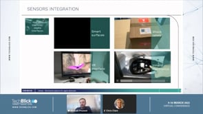
There are many ranging underwater sound detection to vital signs monitoring to micrphones. In this short video, Mickaël Pruvost, PhD from Piezotech, Arkema Group showcases a breadth of applications. But first some background: Piezotech has two types of materials 1) P(VDF-co-TrFE) is a interested fluorinated copolymer able to convert mechanical demonstrations into transient electrical signals and vice versa. It is also sensitive to temperature variations through the pyroelectric effect. It can thus act as an excellent transducer of motion - from body motion to acoustic waves- into electrical signals 2) The terpolymer versions (P(VDF-TrFE-CFE/CTFE) are ale to also convert electrical signals into large deformation via the electrostriction effect. Here, larger movements can be produced compared to the co-polymer versions, and so this is better suited to actuation applications. These materials are produced as powders which are then formulated into printable inks. The inks will need to sandiwched with two conductive (Ag, PEDOT, etc) electrodes and are then annealed and (in the case of FC coplymers) poled to produce piezoelectric properties These materials are thus able to produce flexible, thin sensors and actuators on a variety of substrates printed into arbitary shapes. They are very robust. For example, they survive 1000hrs @105C and 85%RH, do not degrade under hot water test (one hour under 99,9C), and withstand thermal shock test (30min @-40C followed by +85C for 11 days!). Furthermore, they show no degradation after 4million bending and 2.5million pressure cycles! So what are the actual applications of this very unique material? The video below explains many demonstrator and commercial product examples. These include Vital signs monitoring in smar insoles, pulse wave monitoring, and hear beat/breadth monitoring in bed sheets Human machine/object interfaces: smart poeple counting and perhaps energy harvesting surfaces; shock labels, VR interfaces, etc Acoustics: accoustic patten detector, guitar tuner, mobile phone finger print recognition, underwater military equipment, Printed speakers
- QD-Si Image Sensors- beating InGaAs and SiGe in the NIR and SWIR regions with 1.62-2.2um pixel pitch
It took roughly 20 years of R&D to commercialize colloidal quantum dots (CQD) image sensors, which are the first commercial products in the marketplace to use CQDs in electro-active devices in contrast to all of the other current products that use CQDs in photoluminescence mode. First, why quantum dots? The particle size of PbS QDs can be tuned to absorb thoughout the SWIR region spanning from 1000nm to 2500nm. This is shown in slide below, showing also that these QDs can also absorb in the NIR, visible, and UV regions at the same time. Second, why quantum dots + silicon? Obviously the most advanced imaging technology is based on silicon. However, silicon is not sensitive to NIR and SWIR. As such, InGaAs and SiGe sensors have taken hold of this market. However, they are often expensive and their heterogenous integration with silicon read-out circuity (ROIC) can add to complexity and limit pixel sizes/pitches although advances in Cu-Cu bonding may change this. As shown in the slide below, The QDs can be spin coated atop a 300mm silicon wafer. Single PbS QDs are formed into thin QD films with a ligand matrix. Out of this, a QF (quantum film) photodiode if formed with top and bottom electrodes (which must be transparent to a broad light spectrum). These QD photodiodes are formed atop the BEOL of a top-side illuminated image sensor. Cu vias are then used to connect the QD layer to the image sensor. In addition to bringing silicon image sensor technology to the NIR/SWIR spectrum, the QD technology can also enable 100% fill factor and help shrink a complex global shutter pixel (which otherwise would need a larger space for the photodiode) In this study, to be presented at TechBlick's Quantum Dot and microLED conference on 30Nov-1Dec, Jonathan Steckel from ST will outline the state-of-the-art, showing how 1.62-2.2um pixel pitches have been demonstrated on 300mm wafers. The quantum efficiency (QE) is >60% (940-1400nm) To learn more join Jonathan and many other world-class speakers on 30Nov-1Dec online in TechBlick's interactive and engagement platform vist here
- IGZO TFTs bent >1,000,000 cycles at 1mm radius - how was this made possible?
Toppan Inc earlier in the year reported that it has developed an IGZO TFT technology able to withstand >1M bending cycles @1mm radius. This is an incredible result (for reference: foldable smart phone has a radius of 3mm). This is a fantastic result. Manabu Ito discussed at a TechBlick conference how this was achieved. Here, we offer a summary of the key technical innovations. 1) Make dielectric organic: In general many have focused on organic semiconductors to promote bendability of TFT arrays. However, the active channel is an oder of magnitute thinner than the dielectric, and thus has a far less important influence on bendability. In this work, Toppan switched to an organic gate insulator and etch stopper material (PVP based??) instead of the glassic SiOx, SiNx or AlOx materials. 2) Plasma resist layer: As shown in the slide below, the deposition of the IGZO layer directly on the organic dielectric (botton gate device architecture) damages the surface, thus leading to very poor TFT charactersitics with low mobility, limited on/off ratio, higher threshold voltage, and poor sub-threshold characteristics. To overcome this, Ito-san et al deposited a just 7nm thin SiOx layer using ALD. This layer helps improve interfacial properties and also protects the underlying organic dielectric layer during the position. Indeed, as shown below, this results in excellent transfer characteristics for the TFT! 3) Island approach: The 7nm-thin SiO2 layer however cracked after 100k cycles at 1mm radius. The crackes essentially destroyed TFT function. As shown below, to prevent this, they patterned the SiO2 layer such that it existed only below the TFT area. This small change- requiring one additional photolithography step- ensures that the device would be bent more than one million times at a radius of 1mm As shown in the final slide, this works still represents the state-of-the-art work. It does not involve printing or additive electronics, but enables one to design and produce truely flexible TFT arrays able to follow extreme curvature. In this project, they comobine a 64pixel TFT array with ferroelectric polymer to form a flexible motion system to detect the motion of swallowing.
- Finally (!) a viable screen-printed copper metallization for back-contact Si photovoltaics (PV)?
Here you can see data - shared at TechBlick in March 2022- that shows rapid sintred Cu nanoparticles are a viable solution that meet most industry requirements. First some background: the PV industry has tremendously progressed with a steep learning curve of 25%, meaning the cost drops 25% everytime the accumulated production capacity doubles. The PV industry itself is now very large (around 183 Gwp in 2021 of new and replacement installation) but how large will it get in a net zero emission scenario in 2050? There will need to be an installed capacity of 20-80 TWp, producing 30-100 PWh of electricity. This will translate into an annual volume of 1-4 TWp/year, showing that there is still much room for expansion and thus innovation Ag is a major cost driver of the PV cell today. Around 15mg/Wp is used in a PERC architecture for bus and finger metallization. Interestingly, not just cost but also availability can be a concern since 50% of today's world mining capacity would only cater for 1 TWp/a. Given these concerns, the industry has long sought to replace Ag with alternatives such as Cu. However, many issues havehindered adoption even in new PV architectures including Cu diffusion into Si, solderability, good adhesion, long term stability, etc etc In this study, Jan Lossen from ISC Konstanz shows that one can meet almost all requirements on a back-contact Si PV when the bus bars are screen printed using Cu nanoparticle pastes from Copprint. It also shows the good outlook for the case when also the fingers are replaced. Slode show shows the difference between PERC and back-contact architecture. In the former, finger and bus bars (BB) on the front side are based on screen printed Ag, whilst Al metallization is used for the rear side. In the latter, the contacts for both polarities are placed on the rear side, thus leaving the front unshaded. If Ag were used this would mean even higher Ag content as both electrodes are Ag based! In this study, the BBs were printed with low-T Ag pastes and various types of Cu pastes dried at 100C and sintered at 300C for 5s. You can see how the line resistance requirements are met by all Cu BB configurations. These BBs have 1.5mm width and 12um height. Furthermore, we see that the Jsc and Voc are not impacted. Climate chamber tests were also carried out, showing NO indication of Cu diffusion in thermal cycle and damp heat tests. The remaining challenge here is the peel force. The slide below shows that one can can solder onto the Cu BBs the peel force is not sufficient, probably because of low adhesion between Cu and cell surface, requiring an ECA. Final slide shows that fingers based Cu pastes also yield good results, suggesting that all Cu-based back-contact Si PVs are possible! Ofer Shochet Dominik Rudolph Andreas Halm Yitzchak (Isaac) Rosen #solarcell #solarpanels #printedelectronics #copper #renewables
- Quad Industries | The advantages and functioning of PTC heaters
Sometimes manufacturers would like to install heating in objects that are difficult to heat. The armrest of your car. Your sporty winter coat. Bags for food delivery. Sleeping bags. All of these are products that are usually influenced by environmental temperature and cannot autonomously create their own level of temperature. Until now. Imagine a fast pleasant temperature in your vehicle, not just coming from your seatback, but also from the side panel, steering wheel or armrest. Think of immediately defrosted mirrors and sensor de-icing that make it safer to drive off right away. Picture a more comfortable dentist appointment because the dentist chair is pleasantly warm. Preheated surgical tables and drapes, pet clothing, baby strollers, a warm rug in your dining room… a lot of objects can create a more satisfying experience when generating heat at once. PTC heaters make all these applications, and many more, possible today. Positive Temperature Coefficient heaters or PTC heaters are electrical resistance heaters whose resistance increases with temperature. If a constant voltage is applied, the heater produces a large amount of heat when its temperature is low and a smaller amount of heat when the temperature rises, until it reaches its peak level or equilibrium point, at which the temperature stays relatively stable. PTC Effect Curve ©Henkel PTC heaters are created by printing conductive ink on a flexible substrate. At first silver is printed as a busbar to conduct current. On top of that PTC ink is printed to create resistant heating zones. This ink has the characteristic to self-regulate at a specific temperature. The advantages are correspondingly obvious: As the temperature regulates itself at the desired maximum, the chances for overheating are significantly reduced. This increases the safety of the heater. The low resistance at low temperature causes a rapid increase in temperature and high resistance at higher temperature before self-regulation kicks in. Thus, a rapid functioning and automatic peak level. The design of the substrates and the printed areas can be adjusted to the shape of the object so hot spots can be avoided and a uniform and flexible heating can be applied underneath very different shapes and materials. As the heaters are printed on thin foils, they are also very light weighted. And since the printing technique is an additive process and no etching process, this technique is more sustainable than most others. The desired maximum temperature is determined by using the right inks. Today, we offer solutions that maintain a constant temperature of 40, 60, 90 or 105°C. Battery heater, 300 x 400 mm, 60°C PTC ink We are the specialists to develop and apply this technology in the form and functionality you envision. But you are the product specialist who will undoubtedly discover new possibilities with this technology. Don't hesitate to ask for more information about how we can develop the right PTC heater together with you.