Search Results
Search this site
1084 results found with an empty search
- Exposing The Anatomy Of Functional Surfaces
Speaker: John Skabardonis | Company: Covestro| Date: 10-11 March 2021 | Full Presentation Driven by the desire for ever more compact and sophisticated devices, increasing demands for improved functionality and for more customization options, OEMs are turning to functional integration. Thin, three-dimensional parts which were previously simply thought of as covers, or “skins” can now incorporate diverse functionality. This presentation will explore different means of achieving the above goals through the use of materials from Covestro. John Skabardonis High-Tech Materials for Electronics @ Covestro Bio John Skabardonis is a Chemist-turned-Marketer-Communicator in the Polycarbonates business unit at Covestro, LLC. He is responsible for technical marketing for electronics, electrical and appliances in the Americas region. John is fascinated by the rapid evolution of technology and is focused on materials and techniques which enable this evolution. He is also intensely interested in social media as a means of helping make information easily accessible. John received a Ph.D. in Physical/Organic Chemistry from Case Western Reserve University. He is a design advocate & a member of the Industrial Designers Society of America, a Distinguished Toastmaster and a chairholder in the Color Marketing Group. Join TechBlick on an annual pass to join all live online conference or online version of onsite conference access library of on-demand talks (600 talks + PDFs) portfolio of expert led masterclass year-round platform https://www.techblick.com/ And do NOT miss our flagship event in Berlin on 17-18 OCT 2023 focused on Reshaping the Future of Electronics. This event attracts 550-600 participants from all the world and offers a superb ambience and dynamic exhibition floor. To learn more visit https://www.techblick.com/electronicsreshaped To see feedback about previous event see https://www.techblick.com/events-agenda
- Heterogenous integration: Aggressive pitch scaling, Cu-Cu bonding, and transition to optical I/O
Heterogenous integration is the key to the future of computing. Here, the limiting factor is often the interconnect density (pitch) as well as bandwidth and energy consumption. Indeed, as we move towards platforms where multiple dies, potentially from different foundries, are all integrated into the same package, the issue becomes extremely important because die-to-die communication becomes the bottleneck. The first slide below are from Intel, presented at a conference in Sept 2021 online. Here, you can see the intended evolution of the technology. First, EMIB was launched. Here, a silicon bridge with <55um pitches serves as a small (2x2mm to 8x8mm) communication link between two separate dies in a package. This approaches is an alternative to the standard silicon interpose technology. Next was the development of Foveros platform, allowing face-to-face integration of dies from different foundries onto a package all connected via silicon base logic die. As you can see, these technology will involve with aggressive pitch scaling and a potential transition to direct Cu-to-Cu bonding from microbumps The second slide shows this trend further. It shows the evolution of interconnect pitch as heterogeneous integration advances. The common technology is flip chip BGA (FCBGA). The pitc here is limited to around >120um. Next, the EMIB was launched. Here, the pitch was reduced to 55um thanks to the silicon bridge technology. Now there is Fovereos which is based on die on wafer technology. The next generation will based on HBI or hybrid bonding These heterogenous integration platforms can enable the integration of dies from different foundries. The challenge is though that each foundry has its own I/O designs, making ease compatibility difficult. It is helpful for the industry to develop common standards to enable a plug-and-play solution The third slide shows the need to transition towards Cu-Cu bonding. As the left chart shows, solder based microbumps can supported the technology until around 15-20um. Beyond this pitch level, a transition to Cu-Cu bonding becomes necessary. With this transition comes the possibility to increase bump density to over 10000/mm2. This is vital so that the I/O size and bandwidth do not limit overall system performance in complex multi-die packages. But will all suffice? The fourth slides show need to transition from Cu bonding to optical I/O technologies. As the comparison table shows, optical I/O (OIO) can increase shoreline density by a factor of4, reaching 1.6 Tb/s/mm. It will also improve power efficiency by some 35%. Finally, as shown in the fifth and final slide, this technology will need to evolve. The current (Sept 2021) demonstration was for an on-package OIO able to achieve >1Tpbs/mm @ 6 pJ/bit. The target is a fully integrated OIO able to achieve 10 Tbps/mm @ just 1pJ/bit conversation. Heterogeneous integration is THE technology space to watch
- Using Advanced Battery Design to Truly Electrify Transportation"
Speaker: Gilad Fisher | Company: Addionics | Date: 9-10 Feb 2022 | Full Presentation As climate change concerns continue to drive interest in clean energy and our daily lives become increasingly digitized and dependent on electronics, electrification has become a widespread trend across almost every industry. The problem is that battery innovation hasn’t kept pace with the electric revolution. Charging time, available capacity, lifetime degradation, and costs are key performance areas that are lacking in batteries today. While most efforts to enhance battery performance to date have been focused on battery chemistry, this has only led to incremental changes over the past 30 years. The key to the next step-change in battery performances lies within its structure. This is what Addionics is doing - changing battery architecture to allow the next step-change in battery performance, to any battery chemistry, existing or emerging. Join TechBlick on an annual pass to join all live online conference or online version of onsite conference access library of on-demand talks (600 talks + PDFs) portfolio of expert led masterclass year-round platform https://www.techblick.com/ Our next battery-related event will take place on 15-16 FEB 2023, covering 1) Solid-State Batteries: Innovations, Promising Start-Ups, & Future Roadmap 2) Battery Materials: Next-Generation & Beyond Lithium Ion The speakers include: General Motors, Graphenix Development, Brookhaven National Laboratory, Fraunhofer IKTS, RWTH Aachen University, Lawrence Livermore National Laboratories, Meta Materials Inc, Skeleton Technologies, Solid State Battery Inc, Argonne National Laboratories, OneD Battery Sciences, VTT, Leyden Jar Technologies B.V., b-Science, Rho Motion, Wevo-Chemie, LiNA Energy, CNM Technologies, Ionblox, Empa, Zinc8 Energy Solutions, Avicenne Energy, Echiontech, South8 Technologies, Basquevolt, NanoXplore, Chasm, Li Metal, Sila Nanotechnologies, Quantumscape (tentative), Fraunhofer ISI, etc https://www.techblick.com/
- Copper NP Scale-up | Warp Knitting E-Textiles | Functional Crystals in Structural Electronics...
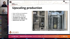
... MicroLEDs, QDs & the Energy Gap |QD-LED & Cd-Free QDs Welcome to this week's edition of our newsletter. First a couple of housekeeping notes: We have begun to cover select display and QD technologies in this newsletter. There are two reasons (1) additive electronics is used in this areas since, for example, QDs are areasolutions processed or microLEDs can be transfer printed, and (2) we are hosting a unique world-class event on microLEDs and QDs on 30 NOV-2 Dec - see schedules here www.TechBlick.com/microLEDs please note that there is strong demand for our onsite event in Eindhoven - the Future of Electronics RESHAPED. The masterclass and tours are almost sold out. Please reserve your spot now if you wish to join us https://www.techblick.com/electronicsreshaped Topics for this edition: Copper Nanoparticle Scale-up | Warp Knitting of E-Textiles | Functional Crystals in Structural Electronics | MicroLEDs and the Energy Gap | Advances in QD-LED and Cd-Free QDs | Stable QDs for microLEDs Will copper nanoparticle inks finally come of age to disrupt the dominance of silver in the conductive paste business? Cost of production has been a major barrier despite the fact that Cu raw material prices are far lower than Ag. This is because this large raw material cost difference does not often get translated into equally large nanoparticle dispersion or ink cost differences. To overcome this issue, Zachary James Davis et al at Teknologisk Institut have scaled up copper nanoparticle production with particle sizes between 30-300nm. As can be seen below, they have already achieved the following: 10+ Kg per day - here the main bottleneck is the heating and mixing of the green ingredients 300 Euros per Kg cost of production which is comparable to the cost of production of Ag nanoparticles. This level of production cost- coupled with much lower raw material cost @36.7 Euro/Kg - can translate into a much lower product cost Inkjet printable inks with DGME-based solvents are able to lay down 0.5-1um thick layers in a single pass achieving 60mOhm per sqr screen printable versions (in development) targeting 50 mOhm/sqr The scale-up of Cu nanoparticle production with automated workflows is an important step towards making Cu ink and paste technology a commercially viable alternative to the dominant Ag inks and pastes. What are the latest status of QD-LED technology and Cd-free QD materials? Fraunhofer-Institut für Angewandte Polymerforschung IAP is a leading research group in the field, always pushing forward the performance boundries of QD technology. As shown below, Armin Wedel shares some updates in his May 2021 TechBlick presentation. Here are some key points: 1) Cd-free QD materials: slide one shows optimized results for QY, FWHM, and PL of blue, green, and red QDs based on Cd-free chemistries. The B, G, and R QDs consist of ZnTeSe/ZnSe/ZnS, InZnP, GaP/ZnSe/ZnS, and InZnP/ZnSe/ZnS core-shell structures, enabling one to approach BT.2020 standards in a non-emissive display. These are very innovative chemistries and core-shell structures: The Te doping in ZnSe core enables very saturated blue colours with high QY (92%); the GaP shell and controlled heating enables the narrowing of the usually wide FWHM of InP-based QDs to 41nm, and the application sodium oleate during core synthesis of R QDs enables even narrower FWHM 2) QDs as colour conversation in microLEDs: Slide two shows that CdSe and InP QDs can be used as colour converters in microLEDs, whilst slide three shows QDs can be stable in a matrix system for uLEDs. QD colour conversion is very promising for 3) Emissive QD-LEDs: OLED max luminance and EQE still beat that of emissive QD-LEDs which are far less mature. CdSe have improved over the years, offering excellent performance, but Cd toxicity is a concern. The performance of InP QD-LEDs lags far behind in terms of Cd/m2, EQE, and lifetime. This is an exciting development area. Indeed, there is already a roadmap from RGB OLED or WOLED to full inkjet printed (IJP) emissive QD-LED via the development and scale up of Blue OLED + IJP (R,G) QD Conversation technology. To learn more join the world's firfirst-everst ever microLED and QD event online https://lnkd.in/eDRi5kp2 Integrate electronic circuits into standard textiles using a mass production techniques? Warp knitting is an excellent candidate. It combines weaving and weft knitting, allowing the warp knitted fabrics to have the stability of woven fabrics and the elasticity of knitted ones. This well established technology can enable the integration of complex circuit patterns using functional / conductive fabrics with standard textiles using a mass production technique able to handle many different fibers in the same process. In this short talk, Sophia Krinner KARL MAYER showcases the following amazing technology demonstrators: textile as remote control for commanding a mini robot working mobile phone charger pad based on textiles smart shirt for measuring heart rate, temperature and humidity What are micro-, mini-, and traditional LEDs? Eric Virey - super analyst in the field Yole Group - prepared the below chart, showing the key differences between each. Traditional LEDs come in SMD or through-hole packages and the dies are typically 1mm or larger. This well-established application finds use in general lighting, automotive lighting, and LCD backlights. Min-LEDs are typically smaller than 200um in die size but larger than 50um, and come in SMD or CoB (chip-on-board) packages. They are currently commercial and find applications in LCD and keyboard backlights, narrow-pixel pitch LED direct view LEDs, and other sectors. In the LCD sector, they are suited to provide local dimining to imrpove contrast, making LCDs more like OLEDs on this feature. and micro-LEDs are very small, typically smaller than 50um. The size of the microLEDs is expected to shrink further as the technology progresses to reduce LED cost (more LEDs per wafer) and transfer cost/time (e.g., more LEDs transfered within the same stamp). Evidently each class of LEDs is very different in every sense from growth techniques to performance to application. Join TechBlick's microLED event to hear Eric and 30 other top-class speakers covering every aspects of microLED industry https://lnkd.in/eDRi5kp2 Stable RoHS-compliant Cd-free QDs for microLEDs? This technology is required to simplify the manufacturing of microLEDs- this way one need not transfer R G B uLEDs but can only transfer the already efficient blue uLEDs and achieve RGB color via red and green QD color conversation. There are of course multiple material challenges including achieving Cd-free RoHS-compliant green and red QDs with (1) high enough thermal and light stability for direct integration into microLED chips/dies, (2) high blue absorbance even at low thicknesses to prevent blue color leakage, (3) narrow FWHM and high QY, (4) low self excitation, etc QustomDot -spin off from Zeger Hens group at Ghent University- is making excellent progress in this field. They have a novel high-controlled synthesis process for InP based QDs. Last year, at TechBlick they shared some interesting stability data for QD integration in macro and thin film LEDs. These results are shown in the slides below. They show a clear pathway towards development of QDs for direct on-uLED integration The 500um thick QD level integrated on a macro LED shows >>300hours stability even under 1W/cm2, and a 100-150um QD thin film under 130mW/cm2 also shows >>1500 hours photostability in insert conditions These are results from last year. To hear the latest developments from QustomDot on QD-on-microLED please join TechBlick's microLED and QD event. Check the world-class agenda at www.TechBlick.com/microLEDs Why can microLED technology can help narrow the energy gap in electronic devices? @Khaled Ahmed from Intel Corporation offered a data-rich unique assessment at TechBlick's display event in 2021. The first slide shows the battery gap- Ahmed has collected data by year showing that power demand of phones far exceeds the power supply level of batteries, creating a "battery gap" which widens each year as more power-hungry features are added whilst battery technologies imporves only incrementally. Some 70% of power consumption of a mobile phone or tablet is by the display, showing its outsize importance in shrinking this gap. The second slide shows the improvements in the efficiency (lm/W) of 'released' OLED devices per year. The OLED efficiency has clearly plateaued in produced or released products. The backdot represents the projected potential of microLEDs, showing how the microLED technology can be a game changer. The third slide shows that there is a gap between EQE of laboratory OLEDs and that of released products. The origins are not clear but likely involve trade-offs neccessary in production and trade-offs between lifetime stability and EQE. The four side compares the efficiency of GaNw LEDs at various wavelenghts vs organic LEDs (from previous slides). It shows that GaN LEDs offer dramatically higher EQE levels compared to OLEDs at all wavelenghts except red. Indeed, there is a red efficiency gap in GaN microLED technology, the filling of which is the subject of intense global R&D This charts clearly demonstrate that while OLED technology seems to have plateaued and thus will not likely ever overcome the Battery Gap, the emerging microLED technology offers high promise to do us. Of course development and manufacturing of microLEDs involves other challenges such as rapid transfer as well as high-yield production which we will disucss elsewhere. To learn more about microLED technologies, join the world's first ever specialist technology on the topic. Check out the world-class agenda at https://lnkd.in/eDRi5kp2 Functional crystals meet printed electronics meet structural/embedded electronics meet automotive interiors? Rafael Michalczuk howcases fantastic and beautiful demonstrators combining all these technologies. Here, in collaboration with PolyIC and Kurz, they showcase beautiful interactive smart surfaces with integrated functional crystals for automotive. The embedded (hidden) electronics technology is from Kurz (based on PolyIC technology) based on its R2R metal mesh technology (10um linewidth and 100um spacing with ultrathin (100 nm) layers of printed Ag nanoparticles) together with their so-called Functional Foil Bonding, which enables these metal mesh films to be integrated on the back of shaped plastic parts together with decoration layers. This creates part with electronics seamlessly integrated within the curved or 3D shaped part SWAROVSKI I provides the beautiful functional crystals which enhance the aesthetics but also allow for continued touch and optical interaction with the underlying electronics. Spaces are limited BOOK NOW to join us in Eindhoven
- 3 Biggest Challenges in New Generation Printed Microelectronics That XTPL Will Help You Overcome.
Additive manufacturing (AM) offers tremendous possibilities for the fabrication of next-generation microelectronic devices, including lower cost and simplicity. Yet, there are several challenges to the widespread use of AM techniques for microfabrication. The miniaturization trend requires printing ultra-thin and highly conductive interconnects on complex 3D topographies and heterogeneous substrates. XTPL’s Printing Technology tackles these challenges. We demonstrate Ultra-Precise Deposition (UPD), a versatile approach to printing micrometric conductive and non-conductive structures on various rigid and flexible substrates (see: Łysień et al. High-resolution deposition of conductive and insulating materials at micrometer scale on complex substrates. Sci Rep 12, 9327 (2022). https://doi.org/10.1038/s41598-022-13352-5). UPD allows maskless deposition of highly-concentrated silver, copper, and gold pastes, up to 85 wt. % of solid content. The printed feature size can be as small as 1 µm, and the maximum electrical conductivity obtained in this range is around 45% of the bulk material. The UPD process is based on a direct extrusion of ink using pressure. Simultaneous optimisation of the ink, printing nozzle and process parameters allows for extrusion of high viscosity inks using nozzles with a diameter as small as 1 µm. Thanks to these features, UPD allows to achieve results beyond the reach of other AM techniques: 1) printing on 3D topographies for advanced packaging; 2) printing structures for high-frequency signals, for example, the antenna on chip and 5G/6G communication; 3) printing flexible devices, like sensors, using both high and low viscosity materials (10-2.5M cP) with a wide range of feature size (1-200 um linewidth). Advanced packaging: printing on 3D topographies Challenge: conductivity drop on high angled sidewalls The possibility of printing 3D interconnections is particularly interesting for system integration and packaging, including hybrid electronics (combining printed and silicon technologies). For example, we print repeatable and continuous silver lines with a width of 15 µm on a step with a height of 150 µm. Therefore, the step height is ten times the width of the lines. Here we overcome a typical problem for other AM techniques: the material does not flow down when printed on steps and can be directly deposited on a vertical sidewall. Repeatable and continuous silver lines with a width of 15 µm are printed on the step with a height of 150 µm. There is a clear market need for heterogeneous integration for high-performance flexible hybrid electronics that combine printed electronics and silicon technology. The challenge is the integration of flexible ultra-thin chips (UTCs) on flexible foils as they are too fragile for conventional bonding methods. In this regard, UTCs printed on the flexible PCB using XTPL’s microdispensing system show robust device performance under bending conditions, indicating the high reliability of both the chip thinning and bonding methods. The ability to print such interconnectors using the UPD approach has been successfully demonstrated in the literature (see: Ma, S., Kumaresan, Y., Dahiya, A. S., Dahiya, R., Ultra-Thin Chips with Printed Interconnects on Flexible Foils. Adv. Electron. Mater. 2022, 0, 2101029. https://doi.org/10.1002/aelm.202101029): to fabricate flexible ultra-thin MOSFET chip, thinned chip was attached to a flexible PCB and interconnections were printed between the chip and the PCB. This work demonstrated the ability of the UPD technology to connect fragile ultra-thin chips without damaging them, as well as the ability to print interconnections resistive to bending on flexible substrates. Printing structures for high-frequency signals Challenge: high-frequency signal losses caused by poor geometrical homogeneity and structure integrity Samples printed using UPD have unique features important for high-frequency applications: high surface smoothness, constant linewidth, and constant linespace, which limits signal losses. Therefore, UPD gains competitive advantages over other additive manufacturing technologies. Aerosol Jet Printing is limited to 20 µm gap size because of overspray. Moreover, the appearance of the satellite droplets around the printed signal line will produce radiation on the substrate. XTPL’s UPD approach gives printed structures tailored for signals above 300 GHz. Apart from the interline gaps limitation, the common problems are the high roughness of deposited structures (limiting the transmission frequency) and low adhesion to the substrate. UPD deals with these issues: printed silver lines are smooth, and adhesion to a wide range of substrates is very high. The substrate types include glass, silicon, flexible foils, and RO4003. Example silver lines printed on a PEN foil. The line width is 3.2 µm, and the interline distance is 0.7 µm (a distant view of the sample is in the inset). Printing flexible devices: sensors Challenge: using both high and low viscosity materials within single printing method The unique features of the UPD technique for biosensing applications include 1) deposition of both high-viscosity and low-viscosity 3rd party materials (suitable for functional materials and bio-probes); 2) Low-cost and disposable needles that are easy to change to avoid contamination between the various functionalization steps (e.g., antibody/ethanolamine/BSA); 3) Material cost reduction: deposition of micro-areas or micro-dots for matrix system fabrication (like ELISA plate) minimizing the amount of bio-liquid required. An example design for bio-sensing applications. The UPD approach answers the critical challenges in the fabrication of high-density microelectronics: high-resolution printing of various materials on complex substrates. The essential feature of UPD is the ability to print high-viscosity inks using nozzles with a diameter of the order of micrometers. It is possible to obtain structures with arbitrary shapes, including lines, dots, crosses, and meshes. The printed feature size is as small as 1 micrometer with electrical conductivity up to 45% of bulk value. UPD can become an indispensable tool for rapid prototyping and microfabrication thanks to these features. Conclusions The printing technology developed by XTPL is bringing an enabling approach for applications which cannot be done with known subtractive methods and for use-cases, where other additive approaches cannot fulfill all the requirements. Together with strong industry partners, XTPL is in the technology scaling up process, providing solution compatibility with production automation and throughput requirements. The unique approach introduced by the XTPL is also available for R&D and prototyping centres (both in companies and academia) thanks to the Delta Printing System, which is commercially available since late 2020 and today has a rapidly growing user network globally. The device is highly rated by the current customers due to a very high versatility of potential applications for the technology, high freedom to operate with the printing system and outstanding customer support offered by XTPL. Connect with our team at xtpl.com or sales@xtpl.com to learn more about the technology Ultra-Precise Deposition technology and the Delta Printing System!
- High resolution 3600ppi full color Silicon Display for AR glasses and HMD
“Silicon” Displays with an incredible 3600ppifull color using microLED and QD technology? Sharp (HIRANO Yasuakie et al) will join us from Japan to explain this technology at the upcoming TechBlick event on microLEDs and quantum dots (www.TechBlick.com.microLEDs). As shown in the slide below, first blue-only uLEDs are formed on a sapphire substrate. Here, one LED array contains 352 x 198 micro LED dies of 24 um x 8 um in size. In parallel, an LSI chip containing the driving circuitry is formed on a silicon wafer. Here, the cathode (N-type electrode) and anode (P-type electrode) are fabricated for each micro LED die to apply driving voltage independently to each die. The Au bump electrodes are fabricated in accordance with the pitch of the LED dies. The two substrates are flip-chip bonded using Au-Au bonding. Here one can already see the parallel to the silicon and optoelectronic industry (vs. the traditional thin film display industry!). Next, the sapphire layer is removed via laser lift off. Finally, Cd-free quantum dots (green and red) are deposited atop the microLED dies to enable R G color conversion. This way one achieves RGB colors The device architecture is shown in slide 2- here one can see the location of GaN uLED dies, Au bumps, as well as light shielding walls and quantum dots (QDs). This way, a full color 1,053 ppi display is formed. However, given the small size of the emissive area of uLEDs, the brightness is low. An innovative solution here is to switch from individual driving cathode electrodes to a common one, thus freeing up more spaces for uLEDs. As shown in slide three, the light emission in one pixel was improved from 23% to 38%. As a result, brightness of 11 knits was achieved. This is an excellent progress. Of course, it is not the final game as even at 11 knits the brightness is not yet not sufficient for outdoor AR applications. Join us and your industry peers on 30 NOV – 1 DEC 2022 at our first-ever specialist microLED and QD event to hear more about this technology from Yasuakie-san et al: www.TechBlick.com/microLEDs
- How lasers help in MicroLED display production?
How lasers help in MicroLED display production? One of the biggest manufacturing challenges in uLED display production is the transfer step given the speed and yield requirements. As shown in the slides below by Oliver Haupt from Coherent Inc., lasers can play an important role in this step, both when all three colors (R G B) microLEDs and also when only blue microLEDs need to be transferred. To learn more join TechBlick's first ever specialist event on microLEDs on 30 NOV - 1 Dec where Oliver will present this technology www.TechBlick.com/microLEDs The process flow for both cases is shown below. In case of RGB MicroLEDs, first a temporary carrier is attached to the sapphire substrate on which GaN uLEDs are grown. Laser Lift Off (LLO) is deployed to de-bond the sapphire substrate, releasing the carrier wafer with the detached GaN microLEDs. Next, controlled UV spots are used to release the individual microLEDs onto the final substrate holding the TFT active backplane layers. These process can be repeated three times, each time for a different uLED color. In all steps, of course, excellent and optimized control of the laser profile/parameters in harmony with the right adhesive material properties are required. In the case of blue-only microLEDs, the final backplane substrate is brought into contact with the GaN sapphire substrate. The GaN uLEDs transfer to the final substrate via the LLO process. Three color capability is then achieved by color conversation, e.g., QDs or small-sized phosphors The results show the example of microLED RGVB transfer. The parameters are shown in the slide including microLED size, pitch, laser energy density, donor-receiver distance, etc. It can be shown that a different color is transferred with each shot. Thus, in three shots all R G B microLEDs are placed at the right spot! As the subset in slide 2 shows, the laser can in each step/shot process an area of roughly 2.83cm2. To learn more join our world-class event on microLEDs and QDs. More info on www.TechBlick.com/microLEDs #microLED #quantumdot #laser #sapphire #GaN #displays #displaytechnologies #liftoff #uv #backplane #activematrix
- Eastprint | Wearable Biosensors
Contact: Rick Ramos, Marketing & Inside Sales Engineer – Eastprint Inc. Email: rramos@eastprint.com Website: https://www.eastprint.com/index.html Introduction: As wearable electronic devices continue to be more and more prevalent, it becomes an ever-greater challenge for companies that manufacture them to keep their competitive edge. It is vitally important for manufacturers that each device is effective, cost-efficient and reflects the highest quality available. Mass producing wearable biosensors: To cost effectively mass produce wearable biosensors, vertical integration and assembly operations is key. Having the ability to print conductive inks on flexible substrates and fully perform converting operations (such as lamination of medical grade hydrocolloids, adhesives, non-woven and foam layers, hydrogel dispensing and or placement and final packaging) in SMT components and any connections on the non-patient side of the patch (ensures patient comfort). Have been successful in .010” diameter via hole print filling in order to have continuity between skin contact and a assumed communication device. Technologies Used to Manufacture Biosensors Process for manufacturing biosensors employ screen printing, laser cutting, lamination, and adhesives. Screen printing of various conductive inks, such as but not limited to silver, silver/silver-chloride, carbon, zinc, gold, dielectric, etc. In addition, Surface-Mount Technology (SMT) is used if components are required. There are several key converting processes, including die-cutting, lamination of medical grade foams and adhesives, as well as the dispensing and placement of medical grade hydrogels and final packaging. The role of printing through holes methods, which allow for connections between the top and bottom printed circuits and up to 6 layers per side. Majority of applications, biosensor manufacturing involves a supply chain of companies since few companies possess all the necessary capabilities. Required functions in detail as follows: Circuit/Electrode printing Sheet or R2R Typically, 2 to 5 print passes Oven drying or UV curing after each print pass Oven dwell typically ≤10 minutes ≤140°C Slip sheet or interleaf may be required to prevent ink rub-off since carbon inks tend to be soft and transfer to backside of substrate when stacked or wound in rolls Routine in-process measurements to confirm conformance to agreed dimensional, ink thickness and electrical specifications Patterning of spacer/adhesive layer One or combination of SRD, Rotary, Match Metal and/or Laser Patterning of lid or top layer Same as spacer/adhesive Dispensing & drying/conditioning of functional material This is where most of the intellectual property (IP) exists and is often performed by the OEM. This is changing as more medical converters are adding dispense capability in an effort to add value Laminating Cold with pressure sensitive adhesive (PSA) or heated (hot melt) Performed by OEM or converter Option – Cartridge or Cassette type configuration Application may skip lamination process and instead die cut individual sensor circuits and install them into an injection molded plastic microfluidic cartridge or cassette. Sheet/Roll to Cards Large format cut down to rectangular card format (sensors nested 1 row x TBD across) for compatibility with commercially available strip singulation equipment Singulation Individual sensors are typically slit from cards into individual test strips Packaging Singulated test strips placed in plastic vials – often having inside walls lined with a desiccant. Screw or snap cap installed, followed by application of label
- Warp knitting: Integrate electronic circuits into standard textiles using mass production techniques
Integrated electronic circuits into standard textiles using mass production techniques? Warp knitting is an excellent candidate. It combines weaving and weft knitting, allowing the warp knitted fabrics to have the stability of woven fabrics and the elasticity of knitted ones. This well established technology can enable the integration of complex circuit patterns using functional / conductive fabrics with standard textiles using mass production techniques. In this short talk, Sophia Krinner @Karl Mayer showcases the following technology demonstrators: 1- textile as remote control for commanding a mini robot 2- working mobile phone charger pad based on textiles 3- smart shirt for measuring heart rate, temperature and humidity
- Functional crystals meet printed electronics meet structural electronics meet automotive interiors?
Rafael Michalczuk howcases fantastic and beautiful demonstrators combining all these technologies. Here, in collaboration with PolyIC and Kurz, they showcase beautiful interactive smart surfaces with integrated functional crystals for automotive. The embedded (hidden) electronics technology is from Kurz (based on PolyIC technology) based on its R2R metal mesh technology (10um linewidth and 100um spacing with ultrathin (100 nm) layers of printed Ag nanoparticles) together with their so-called Functional Foil Bonding, which enables these metal mesh films to be integrated on the back of shaped plastic parts together with decoration layers. This creates part with electronics seamlessly integrated within the curved or 3D shaped part SWAROVSKI I provides the beautiful functional crystals which enhance the aesthetics but also allow for continued touch and optical interaction with the underlying electronics. #functionalcrystas #automotiveinteriors #structuralelectronics #inmoldelectronics #HMI #humanmachineinterface
- Scale up Cu nanoparticle to drive down cost of production
Will copper nanoparticle inks finally come of age to disrupt the dominance of silver in the conductive paste business? Cost of production has been a major barrier despite the fact that Cu raw material prices are far lower than Ag. This is because this large raw material cost difference does not often get translated into equally large nanoparticle dispersion or ink costs. To overcome this issue, Zachary James Davis et al at Teknologisk Institut have scaled up copper nanoparticle production with particle sizes between 30-300nm. As can be seen below, they have already achieved the following: 1) 10+ Kg per day - here the main bottleneck is the heating and mixing of the green ingredients 2) 300 Euros per Kg cost of production which is comparable to cost of production of Ag nanoparticles. This level of production cost- coupled with much lower raw material cost @36.7 Euro/Kg - can translate into a much lower product cost 3) Inkjet printable inks with DGME based solvents able to lay down 0.5-1um thick layers in a single pass achieving 60mOhm per sqr 4) screen printable versions (in development) targeting 50 mOhm/sqr The scale up of Cu nanoparticle production with automated workflows is an important step towards making Cu ink and paste technology a commercially viable alternative to the dominant Ag inks and pastes #printedelectronics #copper #conductiveinks #nanoparticle TechBlick Torsten Lund-Olesen Anna Krzyzanowska Kasper Vestentoft Christian Rein
- Stable RoHS-compliant Cd-free QDs for microLEDs?
This technology is required to simplify the manufacturing of microLEDs- this way one need not transfer R G B uLEDs but can only transfer the already efficient blue uLEDs and achieve RGB color via red and green QD color conversation. There are of course multiple material challenges including achieving Cd-free RoHS-compliant green and red QDs with (1) high enough thermal and light stability for direct integration into microLED chips/dies, (2) high blue absorbance even at low thicknesses to prevent blue color leakage, (3) narrow FWHM and high QY, (4) low self excitation, etc QustomDot -spin off from Zeger Hens group at Ghent University- is making excellent progress in this field. They have a novel high-controlled synthesis process for InP based QDs. Last year, at TechBlick they shared some interesting stability data for QD integration in macro and thin film LEDs. These results are shown in the slides below. They show a clear pathway towards development of QDs for direct on-uLED integration The 500um thick QD level integrated on a macro LED shows >>300hours stability even under 1W/cm2, and a 100-150um QD thin film under 130mW/cm2 also shows >>1500 hours photostability in insert conditions These are results from last year. To hear the latest developments from QustomDot on QD-on-microLED please join TechBlick's microLED and QD event. Check the world-class agenda at www.TechBlick.com/microLEDs #microLED#miniLED#quantumdot#LED#displays#displaytechnology#RoHS#