



8 August 2022
Fully R2R printed TFTs with highly purified semiconducting SWCNTs?
Printed TFT has been a difficult technology to develop given the complex multi-layer nature of TFTs with their high sensitivity to interfacial and film quality properties. Here (from March 2021), Patrick R. L. Malenfant et al showcases R2R printed TFT sheets with good mobility and low VT variability even over a 10meter print run! Interestingly, SWCNTs have proven to be a good solution for the semiconductor layer of a printed TFT. SWCNTs are grown as a mixture of metallic (70%) and semiconducting (30%) tubes. Since there is no reliable method yet to only grow semiconducting types, one must separate the two. The best technique is based on use of conjugated polymers, which, through repeated rounds of centrifugation, enables one to disperse and thus separate CNTs based on diameter, chirality and type. This way one can obtain highly pure semiconducting-only SWCNT. Indeed, Raymor Industries Inc. is offering such materials already. The separated dispersions are not yet printable inks though. To formulate R2R printable inks, Patrick et al recommend a ligand exchange process to replace the hydrophobic polyfluorenes polymers (left over around the tubes as part of the separation process) with a more hydrophilic polymer. In the video below, Patrick shows that R2R printing of fully TFT is possible with excellent results: the TFTs have mobility range of 0.02-3 cm2/V.s, On/Off ratio of 1E4, and threshold voltage variability of around 6-10% over a 10m R2R print run! This technology shows the...
8 August 2022
Evolution of flexible active matric backplanes to integrate all side circuits and driving ICs?
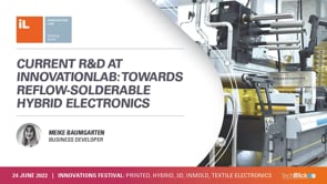
Here, Meike Baumgarten explains how InnovationLab GmbH is evolving the architecture of flexible active matrix backplanes with printed electronics and thinned ICs as part of 2-Horisons project to eliminate all rigid parts. In a conventional set up, the non-pixel-level circuits as well as driver IC sit off-site, linked with the flexible backplane via some connector. In this project, iL has already demonstrated that it can print many of the circuit functions (e.g., multiplexers, decoders) already onto the flexible backplane sheet. This is an important advancement of the technology. The next step of the evolution will be to print also full circuits and fan-outs and place thinned silicon IC/dies onto the flexible active matrix backplane sheet, thus integrating all the electronics into the backplane sheet itself. This is essential for creating very flexible displays and will be an important development in the field. To support this project, and also to generally support flexible hybrid electronics, iL is also developing techniques to solder ICs and SMDs directly onto the substrate with printed metallization. Here, Cu inks are S2S printed to, for example, form NFC on substrates such as PEN, FR4, and PET. Given the non-bulk conductivity of inks, a high dry thickness of 30um is required for printed Cu metallization, which can result in spreading and thus shorting between the pins of ICs. Meike Baumgarten explains various approaches to overcome this challenge To learn more join the Pri...

8 August 2022
Solderable "silver" conductive paste for hybrid electronics compatible with SMT assembly?
Curable silver inks with millisecond curing for rapid R2R printing? In this short 5-min video by Philipp Hoelzl you will learn about both these trends. In particular you will see the following: Solderable Silver Ink: Elantas has developed a silver ink which is resistant up to 200C and compatible with substrates like Kapton. This ink- offering <15 mOhm/s/mill- survives harsh conditions, meaning that it can - together with printable high-T insulators - enable temperature sensors for environments in which inks normally burn! Interestingly, the high temperature nature means that it can also be soldered. Here, you will see prototypes by Kundisch GmbH & Co. KG showing how these silver conductive pastes can be soldered using a low-temperature Sn-Bi-Ag solder with a eutectic temperature of 138C. Here you will see a complex example involving soldered LEDs, NFC function, and touch screen elements with printed metallization on glass. This is an important development because it shows that not only copper inks, but also silver conductive inks can also be soldered, thereby enabling SMT assembly of parts and thus enabling flexible hybrid electronics R2R Silver Conductive Inks: R2R printing is all about speed. Often, the heat curing step (a few min in the oven at >120C) slows the entire process down, and requires long ovens with buffer zones. This is why UV curable inks are desired. However, many UV inks do not meet requirements, especially as the absence of forceful drying, unlike heat curi...

7 August 2022
Novel anode solution: graphene coating on nano silicon
Speaker: Thomas Yang | Company: Sino Applied Technology | Date: 9-10 Feb 2022 | Full Presentation Join TechBlick on an annual pass to join all live online conference or online version of onsite conference access library of on-demand talks (600 talks + PDFs) portfolio of expert led masterclass year-round platform https://www.techblick.com/ Our next battery-related event will take place on 15-16 FEB 2023, covering 1) Solid-State Batteries: Innovations, Promising Start-Ups, & Future Roadmap 2) Battery Materials: Next-Generation & Beyond Lithium Ion The speakers include: General Motors, Graphenix Development, Brookhaven National Laboratory, Fraunhofer IKTS, RWTH Aachen University, Lawrence Livermore National Laboratories, Meta Materials Inc, Skeleton Technologies, Solid State Battery Inc, Argonne National Laboratories, OneD Battery Sciences, VTT, Leyden Jar Technologies B.V., b-Science, Rho Motion, Wevo-Chemie, LiNA Energy, CNM Technologies, Ionblox, Empa, Zinc8 Energy Solutions, Avicenne Energy, Echiontech, South8 Technologies, Basquevolt, NanoXplore, Chasm, Li Metal, Sila Nanotechnologies, Quantumscape (tentative), Fraunhofer ISI, etc https://www.techblick.com/...
8 August 2022
3D formable diffuser substrates for integration of LED lighting with embedded printed electronics?
A prerequisite is often the right formable diffuser substrate! Here you can learn - from Menno Bos- about ultra formable PC-based light diffusion substrates, enabling one to combine LED lighting with embedded printed electronics over 3D surfaces with no heat spots! In the first example, a formable diffusion based on a clear 250um PC is shown, which can be stretched up to 200% (!!) with no edge thinning, enabling extremely complex 3D shapes. Decorative and functional inks can also be directly screen printed on its surface, enabling the integration of decorative patterns and electronic functionalities. This diffuser technology offers high light efficiency (80%) and good light transition (68%). It has many applications and here you will learn about applications in interior ambient lighting, overhead consoles, and exterior lighting. In the second example, Kimoto Europe introduces a new pre-cured stretchable hardcoat film co-extruded with a clear 250um-thick PC . This is a special pre-cured hardcoat surface which offers very high elongations (135/165%) whilst maintaining a good hardness (2-3H) To learn more join Kimoto in Eindhoven on 12-13 OCT 2022 https://www.techblick.com/electronicsreshaped TechBlick Christoph Bosshard #printedelectronics#automotiveinteriors#lighting#3Delectronics#LED#whitegoods#automotivelighting#touchsurfaces#InMoldElectronics#IME...

8 August 2022
Standard printing to securely bridge the gap between physical and digital worlds?
PRISMADE LABS has developed an innovative technology to enable this. They use standard printing machinery with carbon inks to print conductive patterns on almost any substrate (PC, PET, Paper, etc). These conductive patterns act as “touch transformers” converting an input touch signal into a unique signal pattern or signature, which is then read and recognized by a touch sensor like a mobile phone. The unique signal can then authenticate a card or a product or act as a secure trigger between physical and digital world. The compatibility with standard printing techniques makes this approach widely adoptable in almost any sector where printing is used. The lack of electronic parts, unlike NFC or RIFD tags, makes it lower cost and also environmentally friender, especially in high volume and disposable applications The technology sits somewhere between a simple low-cost but unsecure QD code and an expensive but secure electronic recognition system There have already been many examples of commercial success and demonstration including in driving licenses, in marketing compaigns, and in securing bockchain-link collectables, etc In one interesting example (May 2021), Prismade discuss how it enables the Twich streaming community to security print the physical twin of the their unique digital cards (note: the digital cards can be designed by a member of the Twitch community who has earned enough points). There were, according to Prismade, some 50M digital cards designed by May 2021 Fo...

8 August 2022
Reinventing the Wheel? Printing (R)Evolution For A Luxury Brand
Speaker: Rafael Michalczuk | Company: SWAROVSKI| Date: 10-11 March 2021 | Full Presentation Swarovski is innovating since decades in the additive manufacturing domain and printing technologies form an important puzzle piece in the manufacturing processes. But is it now time to reinvent Gutenberg´s invention? As proof-of-concept Swarovski will showcase in the talk different innovations – ranging from additive manufacturing in jewelry, 3D glass printing to 2D/3D printed electronics applications and nano-imprint lithography in various application areas for the luxury brand. Rafael Michalczuk Senior Technology & Funding Manager @ SWAROVSKI Bio Rafael Michalczuk, Senior Technology & Funding Manager at Swarovski, is supporting research, development and innovation projects within interdisciplinary and cross-functional teams at Swarovski, especially with key enabling technologies involved (e.g. additive manufacturing, printed electronics, artificial intelligence, robotics). Additionally he is founder of the innovation & funding consulting agency InnoPotentials. In this capacity he serves a broad portfolio of clients (from startups, SMEs to large companies and R&D institutions) to develop innovative business ideas, secure funding and support the overall innovation journey of the customers. Join TechBlick on an annual pass to join all live online conference or online version of onsite conference access library of on-demand talks (600 talks + PDFs) portfolio of expert led masterclass y...

1 August 2022
Ink-Free Digital Printing | Solder/Adhesive Free Die Bonding | Roadmap for 3DPE | HTL for ...
Ink-Free Digital Printing | Solder/Adhesive Free Die Bonding | Roadmap for 3DPE | HTL for High Performance OPV | OTFTs compatible with LCD ProductionHigh-Performance Before delving into the details of the technology updates for this week, I would like to say that we very excited about our onsite event in Eindhoven, the Netherlands, on 12-13 OCT 2022. The exhibition is long sold out with a long waiting queue, the world-class agenda is announced, and there is very high demand for attendee tickets. You can see the full information here. This is the most important upcoming event in the industry. Next, we will provide updates and insights on a few interesting developments in the world of additive electronics. We will cover (1) dry ink-free digital printing (2) HTL with deep work function (3) roadmap for 3DPE (4) direct die bonding on paper with solder or adhesives (5) liquid wire based on Ga-In-Sn conductive gels (5) OTFT backplanes compatible with LCD production and (6) key steps in printing sub 30um linewidths A dry ink-free digital printing process to deposit multifunctional materials? We recently came across this interesting system, developed by Masoud Mahjouri-Samani, PhD et al Auburn University. Here, as shown below, an excimer laser is focused by lens onto a target. The target is ablated, forming a plume of nanoparticles which then condense onto the substrate to form nanoparticles. The laser system can be used to in situ sinter and crystallize the structure. This dry print...