


9 October 2025
Innovative Interface Materials for Perovskite Photovoltaics
H. Richter, D. Bischoff, E. A. Jackson, R. M. Carty, H. Ghiassi, T. A. Lada, M. J. Ricci, M. Kollosche and P. C. Brookes Nano-C, Inc., 33 Southwest Park, Westwood, MA 02090, USA, email: hrichter@nano-c.com New global energy demand is being driven by vehicle electrification, datacenters, and AI computing. According to IEEE, over 70% of all newly installed energy generation capacity in 2024 came from photovoltaics. Traditional solar cells based on silicon and cadmium telluride were key to this rapid adoption, however, these universal technologies are reaching their practical conversion efficiency. The primary solution to offer a step change in efficiency while promising to reduce the levelized cost of energy (LCOE) comes from the use of perovskite-based solar cells in tandem with traditional technologies. In addition, the implementation of organic thin film PV as well as flexible perovskite PV enables installations and integrations not feasible with traditional glass-based architectures. We are Exhibiting in Berlin. Visit our booth at the TechBlick Perovskite Connect event co-located with the Future of Electronics RESHAPED on 22-23 October 2025 in Berlin . Contact us for your special discount coupon to attend In order to meet increasing global energy demand while also seeking to achieve reductions in global CO₂ emissions, a new generation of organic and perovskite photovoltaics are needed to: a) enhance the performance of existing, e.g., silicon solar PV and b) allow for...

2 October 2025
Why Lab-Scale Roll-to-Roll Coating Is Key to Scalable Fuel Cell Production
Author: Jon E. Carlé, infinityPV ApS, jegc@infintiypv.com How do you take a breakthrough fuel cell material from the lab bench to the factory floor without losing performance, consistency, or time? The answer lies in how you scale your process. While headlines often focus on gigafactories and industrial roll-to-roll (R2R) systems, the real work of scaling starts much earlier. In fact, it starts in the lab. Before any fuel cell can be mass-produced, it must first survive the transition from small-batch experiments to continuous processing, and that transition is where many innovations stumble. The secret to success is not just in the chemistry. It is in recreating real production conditions as early as possible, using lab-scale R2R equipment that mirrors industrial workflows. This article explores why laboratory-scale roll-to-roll fuel cell processing is the cornerstone of scalable production, how it bridges the gap between research and manufacturing, and what choices such as coating methods can make or break your scale-up efforts. Setting the Stage for Scalable Fuel Cell Manufacturing The capability to coat, dry, and assemble fuel cell layers continuously on flexible substrates brings benefits in speed, cost-effectiveness, and uniformity. However, while the long-term promise of roll-to-roll fuel cell production is evident, its success depends greatly on what occurs at the laboratory level. Before materials advance to pilot lines or full production, they must be tested, optim...

22 September 2025
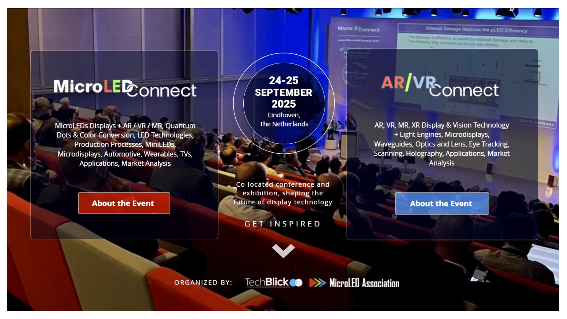
MicroLED’s Technical Turning Point: Why 2025 Is the Year It Gets Real
By Pierre Laboisse, President & CEO of Aledia For more than a decade, microLED technology has captured the imagination of display engineers, semiconductor innovators, and industry analysts. The promise has always been clear: unmatched brightness, durability, and energy efficiency. The challenge has been turning that promise into a mass-market reality, a process that has proven to be complex and slow. Now, in 2025, the pieces are finally coming together. From materials breakthroughs to smarter manufacturing methods, microLED is at a critical inflection point. At Aledia, we have always believed that solving physics was only part of the equation. True success also depends on solving economics, process scalability, and systems integration. This year, momentum is building across all these areas. We are Exhibiting! Visit our booth at the MicroLED Connect & AR/VR Connect in Eindhoven on 24-25 September 2025 At the Core: Materials and Emission Mechanics At Aledia, we are pioneering a fundamentally different approach to microLEDs. Unlike traditional planar technologies, our 3D microLED architecture, built from silicon nanowires, enables far greater light extraction, power efficiency, and manufacturability using existing 200 mm IC manufacturing lines. Our innovations in GaN-on-silicon nanowire growth allow full-color emission from a single material system. This directly addresses the long-standing RGB alignment challenge in lining up red, green, and blue sub-pixels at microscopic sca...

19 September 2025
Losing My Resistance
Low Resistance Carbon Inks, Print Production, Perovskite Cells & Applications. Why carbon inks matter for the future of perovskite solar. GraphEnergyTech Ltd will be presenting at TechBlick Perovskite Connect 2025 in Berlin . Authors: Thomas Baumeler, Chris Jones, chris.jones@graphenergytech.com , GraphEnergyTech Ltd Scaling perovskite solar & the challenge of moving from a reliance on silver The solar industry accounted for approximately 19% of global silver demand in 2024 according to The Silver Institute, with projections suggesting that by 2050 this figure could be at 113% of current production. Silver has cost pressures, price volatility & environmental problems; as well as degradation issues that reduce stability & device lifetime. We are Exhibiting in Berlin. Visit our booth at the TechBlick event on 22-23 October 2025 in Berlin . Contact us for your special discount coupon to attend The case for carbon & graphene Our work focuses on replacing silver with carbon/graphene-based inks. A simple goal of high conductivity, low cost & environmental responsibility. GraphEnergyTech’s printable carbon electrodes are already delivering lower resistance than traditional carbon inks, with up to 87% cost reduction compared with silver and a 97% lower carbon footprint. By tuning our formulations, we are achieving repeatable sheet resistance values below 0.1 Ω/□ at low application weights. These translate into test cells reaching over 21% power conversion efficiency with eng...

6 October 2025
High Performance Silver Inks for Cost-Efficient Manufacturing
Author: Thibaut Soulestin, PhD; Technology Manager Printed Electronics; Henkel Adhesive Technologies; thibaut.soulestin@henkel.com Henkel Adhesive Technologies holds leading market positions worldwide in the industrial and consumer business. As a global leader in the adhesives, sealants, and functional coatings markets, Henkel has developed a large material portfolio of LOCTITE ® conductive inks and coatings. The LOCTITE ® Printed Electronics portfolio offers more than 100 different material solutions. Among those, Henkel silver inks are known to be exceptionally reliable, easy to use, and require only simple handling. This portfolio refers to products with proven superior performance in terms of conductivity and printability. This article focuses on a handful of silver inks to provide insights into the selection of the most cost-effective inks for various applications, such as membrane switches, capacitive touch sensors, heaters, and antennas. It introduces the latest Henkel developments in very high conductive inks with LOCTITE ® ECI 1017 and cost-efficient silver-plated copper inks with the LOCTITE ® ECI 4000 series. Efficient manufacturing of hybrid electronics is also enabled by proven compatibility with a range of electrically conductive adhesives or low-temperature solder pastes. We are Exhibiting in Berlin. Visit our booth at the TechBlick event on 22-23 October 2025 in Berlin . Contact us for your special discount coupon to attend 1. Silver Inks Overview 1.1 Ma...

2 October 2025
Full Program Highlight | The Future of Electronics RESHAPED ECC, Berlin, 22 & 23 OCT 2025
TechBlick’s The Future of Electronics RESHAPED conference and exhibition (22 & 23 OCT 2025, Berlin) is just three weeks away! This year’s agenda once again covers the state-of-the-art across the full innovation spectrum of additive, sustainable, printed, hybrid, R2R, 3D and wearable electronics. In this article, we introduce the conference agenda, summarising the innovations that will be showcased as part of the conference program. The list below does not correspond to actual agenda timings. Please book before 10 OCT 2025 when FINAL early birds end Full agenda | Exhibition floor | Masterclasses Fuji Corporation Inkjet-printed silver nano-inks on UV-curable substrates for multilayer circuits with embedded components. GE Aerospace Additive RF sensors and packaging for aerospace applications rated up to 1000 °C. Lockheed Martin Case study on flexible hybrid electronics adoption, incl. copper additive manufacturing and flexible RF circuits. Valeo Printed and in-mold electronics integration into vehicles, addressing automotive specs and quality demands. Akoneer Laser-processed multilayer glass PCBs for semi-additive semiconductor packaging, demonstrating high-density interconnections on glass substrates. AMAREA Technology Multi-material 3D printing of ceramic components with integrated electronics. CEA-Leti Additive PCB fabrication replacing subtractive methods to enable sustainable electronics. NanoPrintek Inkless nanoparticle-based dry printing without sintering v...
22 September 2025
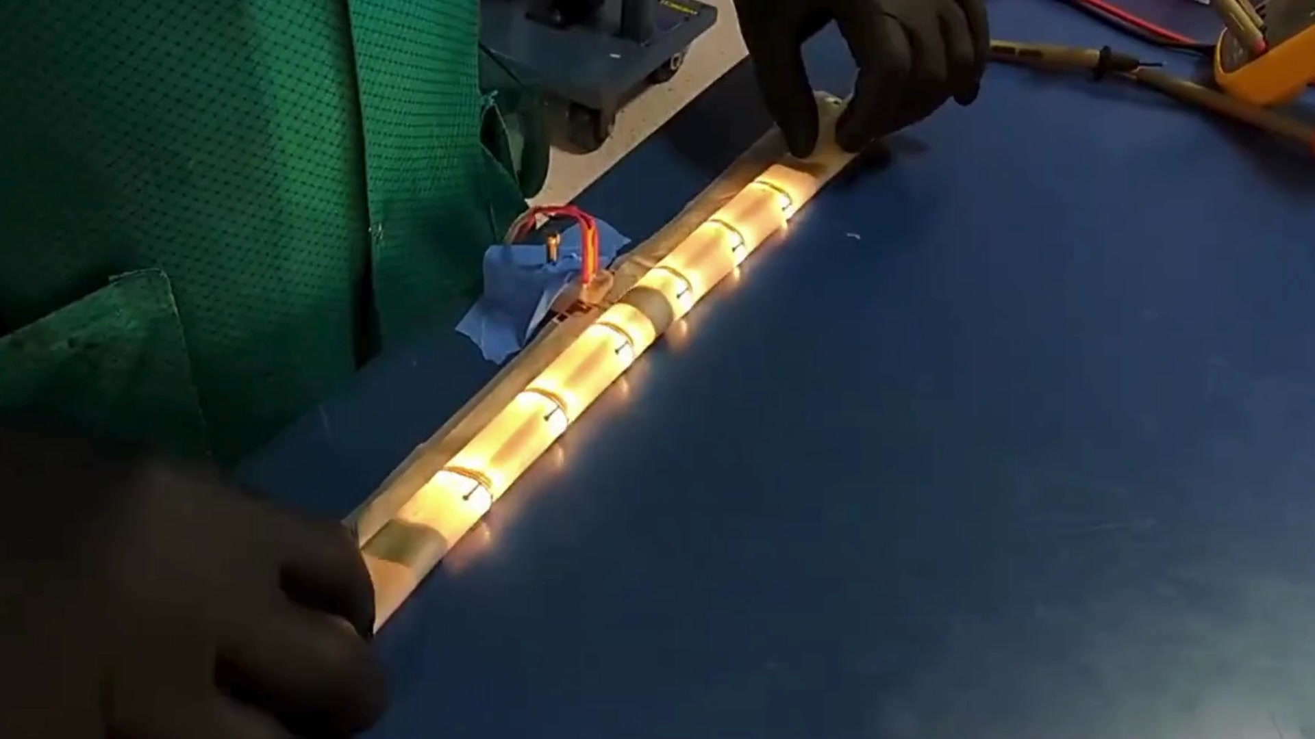
Flexible inks and interconnect for high-performance wearables
Authors: Andrew Stemmerman, John Yundt, Kathy Ritter | SunRay Scientific Inc., Eatontown, NJ USA | andrew@sunrayscientific.com johny@sunrayscientific.com , kathy@sunrayscientific.com SunRay Scientific of Wall Township, NJ, USA has developed a versatile interconnection technology for flexible and stretchable electronics on Thermoplastic Polyurethane (TPU) substrates for wearables. This article will outline the developments of this suite of conductive and dielectric stretchable inks with strong adhesion to mechanically flexible substrates, paired with a high-performance magnetically aligned Anisotropic Conductive Epoxy (ACE). The ACE interconnect material, with ferromagnetic conductive particles aligned along the z-axis, forms vertical conductive pathways to connect multiple component styles to the stretchable circuits on flexible TPU. The ACE additionally provides the strong mechanical bond for the components, with the entire assembly capable of surviving wearables’ wash cycles. We are Exhibiting in Berlin. Visit our booth at the TechBlick event on 22-23 October 2025 in Berlin . Contact us for your special discount coupon to attend Introduction Thermoplastic urethane (TPU) substrates, with flexibility, wear resistance and skin-compatibility, are ideal for wearable electronics applications. Wearables require stretchable circuitry with high density for integration and miniaturization. Printable materials enable low-cost electronic circuit fabrication processes. Sun...
18 September 2025
MicroLED & AR/VR Connect: Full Program
The show will take place next week on 24 & 25 Sept 2025 at the High Tech Campus, Eindhoven, Netherlands. Explore the program here The exhibition spots are all sold out and the registrations have long exceeded the 2024 levels. We hope you will join us and we look forward to seeing you all there. In this article, we introduce the talks that are to be given onsite at the show. Google – Bernard Kress discusses the evolution of light engine technologies for smart eyewear , highlighting design tradeoffs and innovations needed to enable all-day wearable AR glasses . Avegant – Edward Tang contrasts LCoS and MicroLED display engines for AR glasses, examining their respective strengths and tradeoffs as the industry moves toward mainstream adoption. VueReal – Reza Chaji outlines the manufacturing benchmarks microLEDs must achieve —from yield and cost to scalability—to enable transition from niche deployments to broad consumer and industrial adoption . ITEC – Joep Stokkermans introduces XG-Alpha , a flexible lab tool for microLED development that combines laser-based droplet dispensing and die transfer with in-line metrology, dynamic gap control, and optical inspection—aiming for high-yield, cost-effective assembly and paving the way toward next-gen industrial platforms. Aledia – Xavier Hugon presents nanoLED arrays grown on silicon , where GaN nanorods form photonic-crystal structures with intrinsic directive emission and tunable RGB capability, enabling >6000 ppi ultra-compact...