Search Results
Search this site
1084 results found with an empty search
- Cd-free Quantum Dot Colour Converters for MicroLED Applications
MicroLED technology is on its way to replacing traditional display technologies by bringing added value propositions to the consumer market, including high brightness, excellent lifetime, high resolution, and superior efficiency, with applications spanning from wearable devices, augmented/virtual reality, and ultrahigh-definition TVs. To date, challenges in scaling pick-and-place processes and producing highly efficient red and green native microLEDs hamper microLED mass production. A quantum dot (QD) color conversion strategy to produce an RGB display from an array of blue microLEDs is an elegant way to simplify the manufacturing process and to overcome several technological challenges in the mass-transfer process, the display brightness, and the driving electronics. QustomDot’s mission is to bring unmatched colors to micro-LED devices through QD color conversion layers to overcome the challenges above and facilitate market entry of miroLED-based devices. Over the past few years, QustomDot has made a giant leap towards QD resins containing Cd-free RoHS-compliant InP QDs. Our focus has been to formulate QD resins with ultra-high solid loading, excellent shelf life, and processability, adapted for various processing methods, including photolithography, nano-imprint lithography, and high-precision printing methods. In addition to excellent processability, our QD resins result in QD films with high solid loading, excellent absorption at the sub-10 µm thickness, and high conversion efficiency while matching, if not exceeding, the reliability of commercially available InP-based QDs. Our talk will showcase our recent progress towards optimization of our red and green QD resins to obtain color conversion films with optical properties one step closer to fulfilling the challenging requirements of commercial microLED displays.
- Quantica3D | Digital Screen Printing: A Future Game Changer for Printed Electronics Manufacturing
Marcel Strobel | Chief Operating Officer In this talk, we will explore how digital screen printing could potentially revolutionize the manufacturing of printed electronics. Marcel Strobel will introduce NovoJet, an additive manufacturing technology that enables this new method of production. Diving into the benefits that come with it, including the ability to print complex circuitry and its cost-effectiveness for small to medium-sized production runs. By attending this talk, you will gain valuable insights into the current state of the field and the exciting possibilities of digital screen printing in this rapidly evolving industry
- Laser Sintering - a sustainable and rapid post-process for high volume production
Alexander Goerk Business Development Manager Diode lasers are by far the most efficient method to introduce thermal energy into NIR absorbing materials. Fortunately, most conductive inks absorb the 940nm of the Hamamatsu cw SPOLD laser, allowing a homogeneous and rapid sintering result comparable to other thermal post-processing technologies. The use of laser line optics favours scalable, yet highly sustainable high volume production, for example in an R2R machine or ITO Touch display manufacturing. Hamamatsu's own developments in terms of lasers and optics make it possible to adapt to customer-specific requirements, materials and processes. Join us, 77 other exhibitors, 68 speakers and over 600 participants in Berlin (17-18 OCT 2023) to RESHAPE the Future of Electronics, making it Additive, Sustainable, Hybrid, Wearable, and 3D. Explore the programme now https://www.techblick.com/electronicsreshaped
- Warsaw University | Challenges in Printing Ion-Selective Sensors on Skin-Compatible Films
Andrzej Pepłowski R&D Technologist/Project Manager
- TNO Holst | 3D Additive Lithography for Electronics
Jeroen Sol | Scientist Innovator
- TechBlick Announces Screen Printing and In-Mold Structural Electronics Day for 12 May 2023
TechBlick, a leading provider of conferences and workshops focused on emerging technologies, is thrilled to announce its highly anticipated online event in 2023 covering the following important two themes: (1) The Screen Printing Workshop and (2) In-Mold Structural Electronics. You can find more info on www.TechBlick.com The event will take place on 12 May online and will bring together industry experts, researchers, and users to discuss the latest advancements in screen printing and InMold Electronics. Attendees will have the opportunity to learn about the latest innovations and to engage with a panel of experts bringing over 150 years of industry experience together and representing all the key steps in industrial screen printing and in-mold electronics. There will also be unique speed networking opportunities with peers and partners globally. Key activities include Screen Printing Panel: This distinguished panel brings together world-class experts in screen printing for an interactive and insightful discussion. The panelists include: Ron Hayden from RH Solutions LLC with a focus on Screen Printing and Auxiliary Equipment David Eisenbeiss from Kissel + Wolf Group with a focus on emulsion Technology, including the latest Laser Imaging developments Fernando Zicarelli from Fernando's Consulting (formerly at Asada Mesh) with a focus on Mesh Technology and Tooling Erika Rebrosova from Sun Chemical with a focus on functional ink technology Julie Ferrigno from e2ip focusing on applications for fineline screen printing Each panelist will provide a 7-minute overview of their expertise, current state-of-the-art technology, and future developments. There will then be interactive Q&A. InMold Electronics Panel: This distinguished panel brings together world-class experts in InMold Electronics.The panelists include: Antti Keränen, CTO of Tactotek focusing on status of IME process and roadblocks to commercialization Dirk Pophusen from Covestro focusing on status, challenges, and open questions for IME substrates [film aspects] Marius Nolte Covestro focusing on status, challenges, and open questions for IME substrates [resin aspects] Rahul Raut from MacDermid focusing on Ink portfolio challenges and status for complex IME products Robert Boks from Panacol-Elosol GmbH focusing on status and challenges of component attached in IME environment and on 3D shapes Hans-Peter Erfurt from Proell GmbH covering "From Insert Molding to InMold Electronics: Challenges & Opportunities" There will be other presentations from Sefar, RISE Institute of Technology Sweden, and Suzhou Maxwell Technologies, outlining the state of the art. A highlight of the day will be the speed networking sessions where you can connect with other peers and partners for 5-min private one-on-one video conversations before being connected to the next participants For more information about the Screen Printing Workshop and In-Mold Structural Electronics Workshop, visit www.techblick.com or contact Ms. Chris Clare at chris@TechBlick.com TechBlick is a leading provider of conferences and workshops focused on emerging technologies in the fields of electronics, materials, and manufacturing. With a commitment to excellence, TechBlick aims to connect industry experts, researchers, and technology enthusiasts, fostering knowledge exchange and inspiring innovation. For moreinformation,visit www.techblick.com.
- Become a TechBlick speaker on MicroLEDs, QDs, and/or AR/VR/MR Displays?
TechBlick is launching a series of world-class online events on AR/VR/XR Vision Systems, MicroLEDs, and Quantum Dots. We are now curating the agenda for these events and would like to invite you to become a TechBlick speaker! TechBlick has 1600 global members. To give you a sense of our events, you can explore the agenda for our 2022 microLED event here. You can also explore all TechBlick speakers here to give a sense of the high calibre of our events. If you wish to present at any of the following events then please fill out this form https://2cv5l2oxdg7.typeform.com/to/P7KoAs8y 1) AR, VR, and MR Vision Systems: Innovations, Promising Start-Ups, Future Roadmap (26-27 July 2023). You can learn more here 2) Mini- & Micro-LED Displays: Markets, Manufacturing Innovations, Applications, Promising Start-ups (29-NOV to 1 DEC 2023). You can learn more info here 3) Quantum Dots: Material Innovations and Commercial Applications (29-NOV to 1 DEC 2023) You can learn more info here
- Industry Survey: The Future of Screen Printing and InMold Electronics
Industry Survey! We need your input! On 12 May, we have planned a special workshop covering two important themes: (1) Screen Printing for Printed Electronics and (2) InMold Electronics. The event will include: Expert Panel on InMold Electronics: Proell GmbH, Covestro, Panacol, MacDermid, and TactoTek Round Robin Speed Networking Talks on State-of-the-Art in Screen Printing: Suzhou Maxwell, Sefar, and RISE Research Institute Round Robin Speed Networking Expert Panel on Screen Printing: RH Solutions, e2ip, Sun Chemical Corp, Kissel + Wolf Group, and Fernando's Consulting (ex-Asada Mesh) Round Robin Speed Networking You can see the agenda for the event here. To guide the panel discussions, ask the most important questions and raise the most pressing issues, we would like to invite you to fill out this brief and easy industry survey, basically sharing your thoughts, comments or questions. Here is the link to the survey. As a thank you, we will offer you a 200 Euro discount to participate at TechBlick events for 12 months.
- Wearable Ward Monitoring Solutions - GE Healthcare
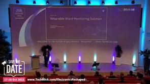
GE Healthcare is a global company that has been operating for many years, with almost 50,000 employees and a revenue of almost 20 billion dollars. The company is best known for its medical imaging devices, but one of its business units, Monitoring Solutions, is focused on manufacturing multi-parameter monitors for operating rooms and intensive care units. Recently, GE Healthcare established a smaller unit that focuses on wearable patient monitoring, which is the department that will be discussed in this video. Patient Monitoring in Hospital: In an intensive care unit, a sedated patient is connected to many cables and tubing to measure various parameters. The nursing staff is interested in knowing whether the tissues are properly oxygenated, whether the medication is correct, and whether other vital organs are functioning well. Therefore, lots of information is required to answer these kinds of questions. On the other hand, in general wards, patients are not monitored at all. The vitals are checked once or twice a day, which is a recognized problem since incidents may happen. Wearable Patient Monitoring: The wearable patient monitoring department of GE Healthcare has recently released a product called the Portrait Mobile Monitoring Solution. It includes two wireless transmitters, one measuring the respiration rate, and the other measuring the blood oxygen level. The system also includes a small mobile phone-like patient monitor that can be used in standalone mode or transmit data to the hospital server. Why Respiration Rate and Blood Oxygen Level? Respiration rate has been recently recognized as a very good early indicator of patient deterioration, and there are a good number of articles on this topic. The respiration rate can be measured in many different ways, but GE Healthcare chose to use bio-impedance, a very traditional way used in EKG devices, to capture the body movement. The reason behind this choice was that it provides much better reliability than other methods like breathing belts. How Was Respiration Rate Measured? To get an accurate respiration rate and low alarm burden, GE Healthcare started by mapping the human body to understand where to get the best possible signals for respiration rate calculation. They used EIT devices to scan the whole body and chose three electrode locations, two leads, or two channels, to capture the thoracic and abdominal breathing effort. Then, on the algorithmic side, GE Healthcare developed an algorithm to remove the cardiogenic component from the impedance signal, which captures everything and makes up near detection very difficult. Conclusion: The wearable patient monitoring solution developed by GE Healthcare provides continuous signals, and the device can alarm on life-threatening events almost immediately. This is very different from wellness devices that can provide very good trend information but are not suitable for medical analysis. The wearable patient monitoring solution is a standalone device that provides a full feature patient monitor and can transmit data to the hospital server. The focus on respiration rate and blood oxygen level is crucial since they are early indicators of patient deterioration, and GE Healthcare used bio-impedance to capture the body movement, providing much better reliability than other methods. To hear more presentations like this one, join TechBlick's The Future of Electronics RESHAPED conference and exhibition in Berlin on 17 & 18 October 2023 - www.TechBlick.Com
- Innovation in Luminous and HMI Surfaces
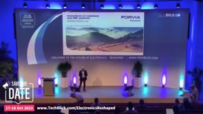
This video looks at the latest innovations in luminous and HMI (human-machine interface) surfaces. Forvia is a tier one automotive company with 150,000 employees and 300 sites worldwide, aiming to become one of the world's largest automotive technology companies. Their innovation team, located in Scotland, focuses on display and HMI product lines, advanced backlight design, and other next-generation solutions. Forvia's ecosystem of startups that have been acquired focuses on developing the next generation of printed electronics. Forvia's projects include working with car manufacturers on exterior lighting with large continuous limited surfaces and pixelation. They are developing large area dynamic lighting with functionality as well as decoration across the IP door panels and even into the roof liner. For the front of the car, they are working on grill elimination and brand lighting, combining backlighting technologies and low-resolution displays. However, their main focus is on the cockpit display. The cockpit display is a large 3D glass panel with screens and other electronic functionalities bonded behind it. Forvia takes standard industry screens and combines them with lighting and other functionalities to create the perception of very large information surfaces while reducing costs. Forvia's light tile technology uses LEDs, printed electronics, and beta inside transparent polymers with optics around them to create homogenous lighting and backlighting of surfaces. By putting the LEDs behind automotive materials and replacing them with Dynamic rgbs. Forvia delivers a dynamic backlighting light with a thin package, providing more space for passengers. By backlighting a range of interesting materials, Forvia achieves a dynamic effect with a small number of LEDs, delivering this dynamic capability at a lower cost and power consumption. They can integrate other functionalities like capacitive switching into the same electrical circuit. Forvia's advancements in luminous and HMI surfaces provide exciting possibilities for the automotive industry. By combining different technologies, they are creating innovative and dynamic lighting and display solutions that improve user experience while reducing costs and power consumption. Hear more talks like this at TechBick's The Future of Electronics RESHAPED conference and exhibition in Berlin on 17 & 18 October, 2023 - see www.TechBlick.com
- Pioneering Printed Electronics with Advanced 3D Printing Technology
Introduction: The rapidly evolving electronics industry demands innovative solutions for quick prototyping and the creation of uniquely shaped devices. An advanced 3D printer, specifically designed for printed electronics, has the potential to revolutionize the sector. In this blog post, we will delve into the key features and capabilities of this groundbreaking 3D printing technology, its applications, and its potential impact on the electronics industry. A Comprehensive 3D Printing Solution for Electronics: The cutting-edge 3D printer in focus offers three essential functions: resin printing, circuit formation, and part mounting. This all-in-one machine can produce printed circuit boards (PCBs) within a day using an additive process, eliminating the need for traditional glass and metal mask tools. This allows users to manufacture even a single piece, making it an ideal choice for rapid prototyping and production of uniquely shaped devices. Innovative Applications and Use Cases: The 3D printer's versatility and potential in the electronics industry have already been demonstrated in various applications. Two of the primary use cases for this advanced technology include: Rapid Prototyping: The 3D printer can manufacture multiple boards simultaneously, reducing the overall production time. The latest iteration of this technology is designed to produce boards in just 16 hours, making it an excellent tool for super rapid prototyping. Unique Shaped Devices: The printer's ability to print resin and form multilayer circuits enables it to create devices with complex structures and shapes. This is particularly useful for designers and engineers looking to create innovative products that require unconventional form factors. State-of-the-Art Materials and Processes: This 3D printer employs low-temperature processes and cutting-edge materials to achieve high-quality, smooth circuitry. In collaboration with chemical suppliers, researchers have developed unique materials with excellent durability, high-temperature resistance, and electrical properties. The low-temperature sintering process used in the printer allows for the production of circuits with smooth surfaces and tight tolerances The proponents of this 3D printing technology believe that additive electronics can have a profound impact on the industry by minimizing waste, reducing transportation energy, accelerating innovation, and contributing to global engineering equality. With this advanced 3D printer, the goal is to revolutionize the printed electronics sector, paving the way for more efficient and eco-friendly manufacturing processes. The advanced 3D printer for electronics is an innovative and versatile solution, offering rapid prototyping and the ability to create uniquely shaped devices. By leveraging state-of-the-art materials and processes, this technology delivers high-quality, smooth circuitry in a short timeframe. The commitment to minimizing waste and fostering innovation makes this 3D printing technology a promising development for the future of the electronics industry. Keywords: advanced 3D printer, printed electronics, rapid prototyping, unique shaped devices, low-temperature processes, additive electronics
- BEYOLEX™ for Soft Circuit Solutions (Panasonic)
Author: Tsuyoshi Takeda, Panasonic The Electronic Materials Business Division of Panasonic Industry Co.,Ltd. (Panasonic) is a premier supplier of electronic materials like printed circuit boards laminates, semiconductor packaging materials, display films and other leading-edge products. Leveraging our core expertise in high-performance thermosetting polymer chemistry, we developed BEYOLEX™, a fully cross-linked, non-silicone, thermosetting stretchable film. BEYOLEX™ is specifically designed as a soft, stretchable, and durable substrate for reliable printed electronics. BEYOLEX™ exhibits superior performance when compared to existing stretchable films like Thermoplastic Polyurethane (TPU) and Polydimethylsiloxane (PDMS) and is under evaluation and qualification for a wide variety of demanding applications. In collaboration with our innovative partners, Panasonic introduces our latest case studies on soft circuit development which is one of the promising applications of BEYOLEX™. Case Study 1: Pliable PCB made with copper sintering ink InnovationLab and Panasonic developed a pliable PCB demonstrator. This device was designed and manufactured by InnovationLab using BEYOLEX™ and sintered copper ink. Generally, the copper inks require a high sintering temperature (>160 °C), which is extremely challenging for TPU. As can be seen in Pic 1, the BEYOLEX™ substrate had no difficulty tolerating the sintering temperature and exhibited no damage from the process. Furthermore, the combination of the high temperature tolerance of BEYOLEX™ and the solderability of the sintered copper ink enabled component mounting with standard solders such as Sn-Bi or SAC305: resulting in reliable and high density assemblies and delivering a functional PCB with more pliability and softness than typical flexible printed circuits (FPCs.) Pic 1: Pliable PCB made by InnovationLab Case Study 2: Stretchable hybrid PCB made using copper ink and stretchable silver paste Kelenn Technology, a leading manufacturer of printing equipment, also makes functional inks that are customized for their printing systems. Using their proprietary Direct Material Deposition (DMD) technology, Kelenn Technology printed land pads with copper ink and circuit traces with stretchable silver-based paste onto BEYOLEX™ film (Pic 2). This hybrid circuit produced a solderable, stretchable PCB configuration that would be difficult to achieve with copper circuitry alone. Definitely, BEYOLEX™ is the only substrate solution for this design. Pic 2: Stretchable PCB made by Kelenn Technology Subsequently, Panasonic engineers reflowed solder paste onto test vehicles prepared by Kelenn Technology. We printed an industry standard SAC305 solder paste and reflowed the part in a Vapor Solder Oven with a temperature of 230°C. We confirmed both the solderability of the copper ink pads provided by Kelenn Technology as well as the mechanical integrity of BEYOLEX™ after soldering (Pic 3). As a result of this test, we believe BEYOLEX™, with sintered copper ink, is a promising solution for solderable, pliable or even stretchable PCB constructions. Pic 3: Soldering on Cu Case study 3: Tackling the challenges of truly stretchable electronics Stretchable silver pastes are an attractive conductor solution for new form factor devices. However, these polymer composite pastes have inherent limitations for forming truly stretchable electronics; typically, the resistance increases significantly with each elongation cycle and these increases are cumulative, climbing with each stretch cycle. A printable Liquid Metal Based Composite developed by University of Coimbra (UoC) is a promising solution to this issue. UoC’s ink exhibits metallic conductivity and much lower resistance change during stretch cycles compared to silver-polymer pastes. Thanks to the lack of plastic deformation of BEYOLEX™, UoC’s ink printed on BEYOLEX™ looks to be a promising combination for truly stretchable electronics requiring repeated stretching (Pic 4). Pic 4: Stretchable LED with capacitive touch by UoC The soft-circuit solutions made with BEYOLEX™ introduced in this article are made by additive printing processes which are generally more environmentally friendly than the conventional subtractive PCB fabrication process. Panasonic’s Electronic Materials Business Division keeps contributing to create value and to society through innovative materials. To learn more about BEYOLEX™, please visit https://industry.panasonic.eu/products/devices/electronic-materials/beyolextm-thermosetting-stretchable-film