Search Results
Search this site
1075 results found with an empty search
- Functional crystals meet printed electronics meet structural electronics meet automotive interiors?
Rafael Michalczuk howcases fantastic and beautiful demonstrators combining all these technologies. Here, in collaboration with PolyIC and Kurz, they showcase beautiful interactive smart surfaces with integrated functional crystals for automotive. The embedded (hidden) electronics technology is from Kurz (based on PolyIC technology) based on its R2R metal mesh technology (10um linewidth and 100um spacing with ultrathin (100 nm) layers of printed Ag nanoparticles) together with their so-called Functional Foil Bonding, which enables these metal mesh films to be integrated on the back of shaped plastic parts together with decoration layers. This creates part with electronics seamlessly integrated within the curved or 3D shaped part SWAROVSKI I provides the beautiful functional crystals which enhance the aesthetics but also allow for continued touch and optical interaction with the underlying electronics. #functionalcrystas #automotiveinteriors #structuralelectronics #inmoldelectronics #HMI #humanmachineinterface
- Scale up Cu nanoparticle to drive down cost of production
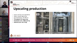
Will copper nanoparticle inks finally come of age to disrupt the dominance of silver in the conductive paste business? Cost of production has been a major barrier despite the fact that Cu raw material prices are far lower than Ag. This is because this large raw material cost difference does not often get translated into equally large nanoparticle dispersion or ink costs. To overcome this issue, Zachary James Davis et al at Teknologisk Institut have scaled up copper nanoparticle production with particle sizes between 30-300nm. As can be seen below, they have already achieved the following: 1) 10+ Kg per day - here the main bottleneck is the heating and mixing of the green ingredients 2) 300 Euros per Kg cost of production which is comparable to cost of production of Ag nanoparticles. This level of production cost- coupled with much lower raw material cost @36.7 Euro/Kg - can translate into a much lower product cost 3) Inkjet printable inks with DGME based solvents able to lay down 0.5-1um thick layers in a single pass achieving 60mOhm per sqr 4) screen printable versions (in development) targeting 50 mOhm/sqr The scale up of Cu nanoparticle production with automated workflows is an important step towards making Cu ink and paste technology a commercially viable alternative to the dominant Ag inks and pastes #printedelectronics #copper #conductiveinks #nanoparticle TechBlick Torsten Lund-Olesen Anna Krzyzanowska Kasper Vestentoft Christian Rein
- Stable RoHS-compliant Cd-free QDs for microLEDs?
This technology is required to simplify the manufacturing of microLEDs- this way one need not transfer R G B uLEDs but can only transfer the already efficient blue uLEDs and achieve RGB color via red and green QD color conversation. There are of course multiple material challenges including achieving Cd-free RoHS-compliant green and red QDs with (1) high enough thermal and light stability for direct integration into microLED chips/dies, (2) high blue absorbance even at low thicknesses to prevent blue color leakage, (3) narrow FWHM and high QY, (4) low self excitation, etc QustomDot -spin off from Zeger Hens group at Ghent University- is making excellent progress in this field. They have a novel high-controlled synthesis process for InP based QDs. Last year, at TechBlick they shared some interesting stability data for QD integration in macro and thin film LEDs. These results are shown in the slides below. They show a clear pathway towards development of QDs for direct on-uLED integration The 500um thick QD level integrated on a macro LED shows >>300hours stability even under 1W/cm2, and a 100-150um QD thin film under 130mW/cm2 also shows >>1500 hours photostability in insert conditions These are results from last year. To hear the latest developments from QustomDot on QD-on-microLED please join TechBlick's microLED and QD event. Check the world-class agenda at www.TechBlick.com/microLEDs #microLED#miniLED#quantumdot#LED#displays#displaytechnology#RoHS#
- What are micro-, mini-, and traditional LEDs?
Eric Virey - super analyst in the field Yole Group - prepared the below chart, showing the difference between each. Traditional LEDs come in SMD or through-hole packages and the dies are typically 1mm or larger. This well-established application finds use in general lighting, automotive lighting, and LCD backlights. Min-LEDs are typically smaller than 200um in die size but larger than 50um, and come in SMD or CoB (chip-on-board) packages. They are currently commercial and find applications in LCD and keyboard backlights, narrow-pixel pitch LED direct view LEDs, and other sectors. In the LCD sector, they are suited to provide local dimining to imrpove contrast, making LCDs more like OLEDs on this feature. and micro-LEDs are very small, typically smaller than 50um. The size of the microLEDs is expected to shrink furter as the technology progress to reduce LED cost (more LEDs per wafer) and transfer cost/time (more LEDs transfered within the same stamp). Evidently each class of LEDs is very different in every sense from growth techniques to performance to application. Join TechBlick's microLED event to hear Eric and 30 other top-class speakers covering every aspects of microLED industry www.TechBlick.com/microLEDs
- What are the latest status of QD-LED technology and Cd-free QD materials?
Fraunhofer-Institut für Angewandte Polymerforschung IAP is a leading research group in the field, always pushing forward the performance boundries of QD technology. As shown below, Armin Wedel shares some updates in his May 2021 TechBlick presentation. Here are some key points: 1) Cd-free QD materials: slide one shows optimized results for QY, FWHM, and PL of blue, green, and red QDs based on Cd-free chemistries. The B, G, and R QDs consist of ZnTeSe/ZnSe/ZnS, InZnP, GaP/ZnSe/ZnS, and InZnP/ZnSe/ZnS core-shell structures, enabling one to approach BT.2020 standards in a non-emissive display. These are very innovative chemistries and core-shell structures: The Te doping in ZnSe core enables very saturated blue colors with high QY (92%); the GaP shell and controlled heating enables the narrowing of the usually wide FWHM of InP-based QDs to 41nm; and the application sodium oleate during core synthesis of R QDs enables even narrower FWHM 2) QDs as color conversation in microLEDs: Slide two shows that CdSe and InP QDs can be used as color converters in microLEDs, whilst slide three shows QDs can be stable in a matrix system for uLEDs. QD color conversion is very promising for 3) Emissive QD-LEDs: OLED max luminance and EQE still beat that of emissive QD-LEDs which are far less mature. CdSe have improved over the years, offering excellent performance, but Cd toxicity is a concern. The performance of InP QD-LEDs lags far behind in terms of Cd/m2, EQE, and lifetime. This is an exciting development area. Indeed, there is already a roadmap from RGB OLED or WOLED to full inkjet printed (IJP) QD-OLED via the development and scale up of Blue OLED + IJP (R,G) QD Conversation technology. To learn more join the world's first ever microLED and QD event online www.TechBlick.com/microLEDs Yohan Kim Manuel Gensler #oled #QD #inkjetprinting #inkjet #QuantumDot #QDOLED #microled #miniled
- Why can microLED technology can help narrow the energy gap in electronic devices?
Why can microLED technology can help narrow the energy gap in electronic devices? @Khaled Ahmed from Intel Corporation offered a data-rich unique assessment at TechBlick's display event in 2021. The first slide shows the battery gap- Ahmed has collected data by year showing that power demand of phones far exceeds the power supply level of batteries, creating a "battery gap" which widens each year as more power-hungry features are added whilst battery technologies imporves only incrementally. Some 70% of power consumption of a mobile phone or tablet is by the display, showing its outsize importance in shrinking this gap. The second slide shows the improvements in the efficiency (lm/W) of 'released' OLED devices per year. The OLED efficiency has clearly plateaued in produced or released products. The backdot represents the projected potential of microLEDs, showing how the microLED technology can be a game changer. The third slide shows that there is a gap between EQE of laboratory OLEDs and that of released products. The origins are not clear but likely involve trade-offs neccessary in production and trade-offs between lifetime stability and EQE. The four side compares the efficiency of GaNw LEDs at various wavelenghts vs organic LEDs (from previous slides). It shows that GaN LEDs offer dramatically higher EQE levels compared to OLEDs at all wavelenghts except red. Indeed, there is a red efficiency gap in GaN microLED technology, the filling of which is the subject of intense global R&D This charts clearly demonstrate that while OLED technology seems to have plateaued and thus will not likely ever overcome the Battery Gap, the emerging microLED technology offers high promise to do us. Of course development and manufacturing of microLEDs involves other challenges such as rapid transfer as well as high-yield production which we will disucss elsewhere To learn more about microLED technologies, join the world's first ever specialist technology on the topic. Check out the world-class agenda at www.TechBlick.com/microLEDs #microled #miniled #qd #quantumdot #displaytechnology #displays #oled #GaN #led
- Morphotonics | Cost-effective Large-area Roll-to-Plate Imprinting
Author: Erhan Ercan | erhan.ercan@morphotonics.com | Jan Matthijs ter Meulen | Kidong Lee Cost-effective mass manufacturing of nano/micron textures is needed to make life-enhancing products commonplace and affordable for consumers. Incorporating such structures via nanoimprinting in higher value-added products like sunlight-readable smartphones, immersive augmented reality glasses, and autonomous-driving-enabling LIDAR sensors will significantly improve our daily lives. Morphotonics, a Dutch nanotechnology company, develops and sells Roll-to-Plate (R2P) imprint technology & equipment. Our market-proven R2P imprint technology enables the mass-manufacturing of such nano/micron-size surface structures over extremely large areas. This leads to unprecedented cost advantages and radically improved products for our customers in the display, sensing, solar, and other deep technology sectors, where such manufacturing precision with cost-competitiveness is the prerequisite for mass-market entry. Morphotonics’ R2P imprint equipment can imprint on substrates with a width of up to 1100 mm (GEN5-size, 1100 x 1300mm2, as shown with Portis 1100 in Figure 1). The process of this R2P imprinting technique is schematically represented in Figure 2. The large area imprint capability enables the manufacturing of a larger number of smaller products in a single imprint step (‘product tiling’). The R2P process can imprint 5 to 20 times more products in comparison to the traditional wafer-scale Nanoimprint Lithography (NIL) systems. Consequently, the cost per product will be significantly lower when using R2P imprinting. At the TechBlick show in Eindhoven, Morphotonics will be offering a guided tour of this technology and its facilities. To learn more about how to join the tour click here. Since the origination of textures is usually limited to wafer scale, upscaling is needed to fabricate the large-area stamps. Morphotonics has developed a proprietary master-upscaling method that enables the upscaling of textures from wafer-scale to beyond 1m2 (an example is shown in Figure 3 related to an SPIE paper published with partners). Next to the master-upscaling method, Morphotonics has also developed large-area flexible working stamps that can last well over 500 imprint cycles, proven in production of commercially available products. This flexible stamp enables a reproducible nanoimprint process. Figure 3. Master-upscaling method example for Augmented Reality (AR) Waveguides Besides offering an unprecedented manufacturing scalability advantage through large-area imprinting, our R2P imprint technology is also quite precise and versatile. Some of the disruptive highlights of the R2P imprint technology are as follows: Accurate: Precise structures with feature sizes from 500 µm to 50 nm, with typical aspect ratios of 1:2-1:3 in micron-scale and up to 1:5 in nano-scale Fast: Imprint cycle times of below 2 minutes in mass production Cost effective: Working stamp ‘Flexible Stamp’ can be reused over 500x, as publicly disclosed by our customers. Minimal resin waste (no spin coating) due to unique resin dispensing method. Versatile: Rigid & flexible substrate (glass, foil, metal) with thickness range of 0.5 – 10 mm Many resin choices - in-house developed, solvent-free resins from 1.4-1.62 refractive index (see Table 1) and co-developed higher refractive index resins from 1.65-1.89 Durable & cost-effective Flexible Stamp choices to match the dimensional stability demands of different product imprints Any nanostructures shape, (see Figure 4) from period gratings of different kinds (blazed, binary, slanted), to microlens arrays, fresnel lenses to nanopillars, and more… Table 1: Morphotonics in-house developed solvent-free UV curable resin choices Figure 4. Several examples of structures that were imprinted using R2P Given many advantages in terms of scaling, replication quality, and versatility that R2P imprint technology can offer, many applications and products can greatly benefit from and become commercially viable using R2P imprint technology. At Morphotonics, we focus on some segments of our addressable market such as displays with high potential that we consider to be our ‘focus’ markets (as shown in Figure 5), while other markets like the high-end lighting could be addressed using R2P imprint technology yet are niche opportunities. Figure 5. Products and applications that can benefit from R2P technology Products such as AR glasses could only become feasible as a consumer products if their relatively large optical eyepieces are manufactured at scale and reasonable costs. Many similar products with the necessary built-in nano/micron textures are beyond the capability of incumbent manufacturing methods, in terms of scale or precision, or both. As such, Morphotonics’ R2P imprint offers an unprecedented alternative to take such products from lab to fab and make them viable consumer-grade products that can improve our daily lives. Morphotonics will be exhibiting at TechBlick on 12-13 OCT 2022 and hosting a live tour of facilities.
- Ynvisible | How to Power Ynvisible's E-Paper Displays with NFC Energy Harvesting
Author: Philip Holgersson (Head of Product) - philip.holgersson@ynvisible.com Ynvisible’s printed E-Paper displays enable a new range of battery-less products. Why? Ynvisible’s E-Paper displays are extremely low power. Low enough to harvest energy from wireless communication interfaces such as NFC. In this article, we’ll provide a practical implementation guide on how NFC can be used to power Ynvisible’s E-Paper displays. Quick Facts About Ynvisible's E-Paper Displays As already mentioned, Ynvisible's printed e-paper displays are ultra-low power. The recommended driving voltage is ±1.5V and one square centimeter active display area requires approximately 1 mJ to activate. This translates to roughly 1-2 µW/cm2 for an always-on display. The displays also have an image memory (or image retention), which is an important parameter for battery-less applications. Ynvisible's standard displays have an image retention time of approximately 5 minutes to 15 minutes. After this period the contrast start to fade and, depending on the use case, a small refresh pulse is required to maintain full contrast. The displays are manufactured using roll-to-roll screen-printing and lamination processes. They are non-toxic, ITO-free, and mainly comprised of PET plastic. The plastic substrate and roll-to-roll production means thin, flexible, scalable, and highly cost-effective displays. Get started using Ynvisible's e-paper display kit. What is NFC? NFC (an acronym for Near Field Communications) a communication protocol for short-distance data exchange between electronic devices. The communication is based on an inductive couple between two antennas. Compared to many other communication interfaces NFC does not need to have built-in power in one of the two communicating devices. Instead, power is harvested from the transmitted signal sent by the NFC reader/writer (such as a smartphone). The most common use-case for NFC is contactless payments. What is required to power Ynvisible E-Paper display with NFC? Fundamentally, an antenna and a diode to rectify the current is all that is required to drive the Ynvisible displays with an NFC signal. Inductive coupling between the transceiver and the antenna will transfer the power from the antenna to the display. The signal must be rectified with, for instance, a rectyfing diode since the display needs DC (direct current) to turn ON. The rectifying diode can be placed in parallel with the display if the display content is designed to fade out shortly after activation. However, an NFC chip would be required if the application requires communication, such as reading an identification code (RFID) or writing data to the device. There are many different versions and manufacturers of these chips, and they have different capabilities. They can be divided into three distinct categories: NFC data storage chips, the transceiver can read and/or write data to the chip. NFC data storage ICs with I2C communication and power output (energy harvesting). These chips can be used to power and/or communicate with an MCU over NFC. NFC chips with embedded processor. These chips can be seen as MCUs with NFC capability, meaning that they have typical MCU capabilities but with the possibility to be powered and/or communicated with through NFC. Examples of these ICs are summarized in the table below: Each IC category requires different implementations of the display. These different implementation methods are presented below: APPROACH 1: CONNECT IN PARALLEL WITH NFC CHIP In this case the display is connected in parallel with the NFC chip. There is no direct interaction between the IC and the display. Both the chip and the display are powered by the NFC signal. In this case, the display will be turned on, independent of the transmitted data. APPROACH 2: POWER OUTPUT OF THE NFC CHIP If the chip is of category 2 the display can be connected to the power output of the chip. As in approach 2 the display will be turned on, independent of the transmitted data. APPROACH 3: MCU IN BETWEEN THE NFC CHIP AND THE DISPLAY Another implementation with chip category 2 is to use a host controller (MCU) in between the chip and the MCU. This enables the MCU to read the data in the NFC chip in turn enabling conditional display driving. This could be useful when the display should be turned on, only if the user has the authority to read the label. APPROACH 4: USE BUILT IN GPIOS TO CONTROL THE DISPLAY Approach 4 is the same as approach 3 but since the MCU capabilities are built into the NFC chips of category 3, no in-between host controller is required. Why NFC-Powered Displays? NFC as a power source is replacing batteries. Batteries are typically limiting the adoption of electronics and printed intelligence in new applications from a cost, sustainability, and recyclability perspective. Ynvisible together with partners and clients are targeting markets including medical technology, smart packaging, smart cards, and brand protection and security devices. The NFC+Display concept is a platform on which sensors and other printed electronics can be added to help shape the future of intelligent objects. Please do not hesitate to contact us if there are any questions. You should also check out our online store to get started.
- Tailor-made REALSi for high-performance Li-ion batteries
Speaker: Chiva Adireddy | Company: Advano | Date: 9-10 Feb 2022 | Full Presentation Today, battery performance is limited by active materials. Graphite storage ability is one of the bottlenecks we can solve using Silicon (Si). Our nanoSi and microSi are based on elemental Si; we call our materials REALSiTM, which is not an oxide, nor produced by Silane gas. Advano converts metallurgical Si, including scrap, into battery-grade REALSiTM using proprietary material science technology. REALSiTM offers tailor-made solutions to both solid-state and liquid-electrolyte batteries. We are open to partnerships to accelerate the commercialization of real Si. The next major evolution in batteries is real Si; our team envisions having REALSiTM in every battery. Join TechBlick on an annual pass to join all live online conference or online version of onsite conference access library of on-demand talks (600 talks + PDFs) portfolio of expert led masterclass year-round platform https://www.techblick.com/ Our next battery-related event will take place on 15-16 FEB 2023, covering 1) Solid-State Batteries: Innovations, Promising Start-Ups, & Future Roadmap 2) Battery Materials: Next-Generation & Beyond Lithium Ion The speakers include: General Motors, Graphenix Development, Brookhaven National Laboratory, Fraunhofer IKTS, RWTH Aachen University, Lawrence Livermore National Laboratories, Meta Materials Inc, Skeleton Technologies, Solid State Battery Inc, Argonne National Laboratories, OneD Battery Sciences, VTT, Leyden Jar Technologies B.V., b-Science, Rho Motion, Wevo-Chemie, LiNA Energy, CNM Technologies, Ionblox, Empa, Zinc8 Energy Solutions, Avicenne Energy, Echiontech, South8 Technologies, Basquevolt, NanoXplore, Chasm, Li Metal, Sila Nanotechnologies, Quantumscape (tentative), Fraunhofer ISI, etc https://www.techblick.com/
- Molecular inks for extreme shapes | Narrowband inkjettable phosphors | R2R sheets of GaNs...
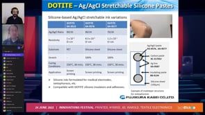
Molecular inks for extreme shapes | Narrowband inkjettable phosphors | R2R sheets of GaNs| Silicone-based AgCl inks| Art of screen making | EMI Sheild House Keeping Note I: TechBlick is now putting together its agenda for its Innovation Showcase Day on 6 June 2022. Email khasha@TechBlick.com if you wish to present. In our last event we had nearly 600 live participants over a 4 hour period! Topics: In this edition, we will cover the following technologies: Molecular inks for extreme shapes | Narrowband inkjet printable phosphor color converters | R2R large area growth of GaN microLEDs | Conformal package-level EMI shielding | Silicone-based stretchable AgCl pastes | Advances in screen printing towards <20um features Molecular particle free inks enable extreme formability and stretchability Molecular particle free inks can offer extreme formability and stretchability, allowing the design and production of 3D shaped and/or in-mold electronics parts with extreme curvatures and complex shapes. Arnold Kell and Julie Ferrigno showcased some unique properties of these inks- together with unique IME possibilities- at a TechBlick conference in May 2021. Some unique feetures are: UV sintering: you can see in the slide below how the transparent clear molecular inks can be UV sintered (x5 times faster than thermal cure). At first, the clear inks absorb very little UV light. However, as Ag particles begin to percipitate out, the absorption grows. The higher absorption in turn raise the temperature, accelerating the sintering and resulting in higher UV absorption. This process continues until the ink is fully sintered and then self stops because then the particles reflect the light back like a mirror. Partial sintering compatible with InMold Electronics: as part of the IME process, a thermoforming step is required. In this step, the substrate temperature is raised in a controlled fashion to soften the material, allowing it to be 3D formed. In the proposed scheme, the printed molecular inks are first only partially cured by UV light. The full sintering then takes place in-situ by the elevated temperature of the 3D thermoforming process. This is an interesting approach because it enables faster curing and also allows one to sinter molecular inks on low-T substrates like PC. Extreme formability: The 3rd slide belows shows comparision of these molecular inks with other standard inks. It shows that these inks can be stretched upto 50% with comparatively little change in resistance. This can be because these printed lines are very thin, and are thus able to follow the contours of the stretched substrate far better than a thicker particle-filled ink/paste Unique shaped: The shapes enabled by IME are often limited by the formability of the inks. These inks can liberate the designer from such limitation, allowing the design and production of complex shapes with extreme curvatures. Here, an award-winning example is showcased by Julie, showing steep curves (see the controlled knob) Phosphors or QDs for color conversion in LCD and microLED ? Which will win? This is an interesting and evolving technology space to watch. James E. Murphy et al from GE Research have developed best-in class narrowband red and green phosphors, and are now evolving the technology towards microLEDs and on-chip integration. The red KSF phosphor is an excellent narrow band color converter for wide color gamut displays. It emits 5 peaks, each of which exhibits an ultra narrow 5-nm FWHM. The main peak is centred around 631nm. It is a stable material under high light flux and high temperature conditions. Indeed, it can be on-chip integrated as a direct replacement for existing yellow phosphors. It is a major commercial success with >19 licensees and >40 BILLION (and growing) KFS-containing LEDs sold worldwide into the display industry. As the slide below, presented at TechBlick July 2021, shows, the KFS technology is evolving. At first in 2014, the average particle size was a 25-30um. It is now down to 3-9um and evolving towards sub-micron and even nano-sized particles, enabling direct integration with microLEDs of today and tomorrow! This is an important technology trend because it brings the QD vs phosphor competition even to the microLED space (previously QDs were the only game in town due to their small size) Furthermore, GE's KSF can now be formulated into air-stable inks based on encapsulant-free phosphors suitable for inkjet printing without nozzle clogging. It means that it can be even printed as a color converter atop microLED, in particular allowing one to use efficient blue microLEDs to create red color and/or only transfer a blue microLED color. James E. Murphy offers also an interesting comparison of Cd-free InP QDs vs KSF for microLEDs. It argues that at very thin films (<10um), QDs are more efficient. However, as the layer is thickened, perhaps to prevent blue color leakage, self-abosrption effects can kick-in, reducing the EQE. Thus, it is argued that KSF clearly wins at >20um thickness given that it has no self absorption. Finally, here is lack of ultra narrowband green phosphors leaving the space open to QDs. In particular, green perovskite QDs are very strong in this field. However, GE is advancing the development of its narrow-band GREEN phosphors. As shown below, these materials enable 100% DCI-P3. The performance is comparable to Beta Sialon but without cross talk with a KSF red emittesr. Furthermore, it offers 100% HTHH stability, enabling direct on-chip integration. Finally, it apepars to have QE levels approach >90%. Of course, just like KFS, it has a slow PL decay time on the order of 90-450um (QD is ns). To learn more about QDs and microLEDs join TechBlick's event on 30NOV-1Dec: www.TechBlick.com/microLEDs R2R grown GaN LEDs and perhaps even GaN/AlGaN HEMT transistors on metal foils instead of expensive small-area sapphire substrates? This could be a breakthrough technology, bringing the robust and efficient inorganic LED technology to large-areas. In microLED displays, it could mean monolithic integration, leading to mobile-sized and large displays manufactured without a wafer-to-substrate transfer step. As shown below, iBeam Materials is developing such technology. It first planarizes a rough metal foil and then uses an ion beam to form a nm-thick layer with aligned grains. This 'template' then acts as the growth substrate in lieu of, say, a sapphire wafer. As seen below, this technology has already been used to demonstrate a functional GaN LED as well as a GaN/AlGaN HEMT. In July 2021 (when the results were presented at TechBlick) the PL was upto 70% of normal LEDs. However, a direct comparison is not yet fair as the standard approach benefits from decades and decades of accumulated know-how and production expertise. Currently, the LEDs are still not done in a R2R fashion, although the 'template' can be R2R manufactured on 20"-wide substrate. The next step of development will involve demonstrating a R2R MOCVD GaN growth. The R2R production of the template is not the bottleneck, but the growth of a thick (5um or so) GaN LED.. Finally, Vladimir Matias argues that this technology has the potential to lower cost of production by a factor x25. A detailed cost analysis is shown below, demonstrating the technical milestones which need to be achieved to enable this cost roadmap. To learn more about this talk and about microLED join TechBlick first-ever specialist event on microLEDs: www.TechBlick.com/microLEDs Particle Free Inks for Conformal EMI Shielding? Conformal EMI shielding is a megatrend on its way to become ubiquitous in electronics. The incumbent process is based on sputtering a tri-layer structure consisting of SUS (stainless steel)- Cu-SUS (total stack is 3-6um typically) on the EMC (epoxy molding compound) of the package. Hikaru Uno from Merck & Melbs LeMieux from Electroninks Incorporated show an alternative based on non-vacuum spray coating of particle-free Ag inks. In these slides, you can see performance analysis and detailed cost analysis/projections. The incumbent (sputtering) is a well established technique with many market reference from the likes of Apple and Samsung. However, it is a vacuum process requiring substantial CapEx investments with a large production footprint. The sputtering deposition rate will also be low given the required film quality. Sputtering is poor at side wall and deep trench coverage, resulting in large thickness variations between the top and side walls. Spraying the EMI shielding can address some issues: it is a non vacuum process with a low Capex and a high unit-per-hour (UPH) throughput and is able to offer uniform side and top wall coverage. The spraying can be used with Ag or Cu nanoparticles. Both nanoparticle techniques though suffer from expensive materials, potential for nozzle clogging and thus production downtime, and even relatively thick required coatings. To overcome these shortcomings, particle-free silver inks can be sprayed. Is this technique effective? The below slides show shielding effective upto 40GHz with 1.2 and 3um coatings. This seems to meet the requirements. Is it reliable? In the slides below you can reliability data showing no measured change in sheet resistance of the package-level coated when subjected to a prolonged duration of harsh conditions Is it cost effective? Sputtering has a high capex cost as well as relatively high labour costs. However, spraying has higher ongoing material consumption costs.The slides below shows that spraying can be a very cost competitive approach Already commercial? It is still in sampling. The main stumbling back is the ever underestimate power of incumbency and already sunk CapEx investments in sputtering lines On the process, as shown below, the package is first pre-treated with plasma. The particle-free ink is then sprayed whilst the packages on the chuck are held at 160-200C. The elevated temperature results in rapid particle formation during the spray. Finally, after spraying, the inks are then cured for 20min@140-160C. There are relatively low curing temperature compared with other particle-free inks on the market. With the first successful market reference using spraying, the market gates will open, lifting all ink-based techniques and making this a part of fast-growing electronic packaging industry Stretchable silicone-based medical devices with AgCl fillers? In general, silicone-basedsheets conductive pastes are rare and the versions with AgCl fillers- needed for many medical wearable applications- are even rarer! David Dewey from FUJIKURA KASEI Co Ltd unveiled this paste for the first time in June at TechBlick. The pastes can offer 1-10 E-4 ohm/sqr when cured at 150C for 30min or so on substrates such as PET or silicone sheet. These inks are compatible with other silicone-based (insulator, adhesive, etc) out of Fujikura's portfolio, enabling one to print complex multi-layer medical wearable devices on stretchable substrates like silicone! To learn more visit www.TechBlick.com or join the industry in Eindhoven on 12-13 OCT 2022 Pushing screen printing below 20um linewidths The progress of screen printing towards fine line printing has been incredible going from 100 µm features before 2010 to 70 µm to 2015 to 40 µm in 2018 and now pushing - in development- towards 20 µm and less. In parallel, the wet thickness of the printed line have gone down from 12um or so in 2018 to now just 4um. In the slides below, Jeffrey Campbell from Sefar Inc. shared examples of screens for fine line printing and showcased fine (<20um) printed features. This slides were presented at TechBlick in March 2022. Advances in all elements of screen making technology have been crucial in driving this development forward. In his presentation at TechBlick Jeff also explained the key technological steps required in enabling and sustaining this trend. These include fine mesh: this is a must as a finer mesh enables higher openings and thinner lines even at high mesh counts. This is shown below. In this slide, you can examples of printed features using 11um stainless steel meshes from Asada Mesh. Narrowing the diameter of the mesh may sound easy, but shaving each micron meter requires three years of intense development!! mesh calendarig: flattening of mesh with rollers improves tensile strenght of the mesh and provides dimensional stability. This enables better control and print-to-print consistency even in fine feature printing emulsion flatting: Reduces the surface roughness of the screen’s surface and reates a more consistent corridor for the paste to travel through. Furthermore, it improves the edge definition of the final print In the slides below you can see many examples of various screens (mesh + emulsion + additional processing like calendering) suited to fineline printing (20um or less). Do NOT forget to secure your ticket to the most important upcoming event on Printed Electronics
- Stretchable silicone-based medical devices with AgCl fillers?
In general, silicone based conductive pastes are rare and the versions with AgCl fillers- needed for many medical wearable applications- are even rarer! David Dewey from FUJIKURA KASEI Co Ltd unveiled this paste for the first time in June at TechBlick. The pastes can offer 1-10 E-4 ohm/sqr when cured at 150C for 30min or so on substrates such as PET or silicone sheet. These inks are compatible with other silicone-based (insulator, adhesive, etc) out of Fujikura's portfolio, enabling one to print complex multi-layer medical wearable devices on stretchable substrates like silicone! To learn more visit www.TechBlick.com or join the industry in Eindhoven on 12-13 OCT 2022 https://www.techblick.com/electronicsreshaped #silicone #stretchable #wearable #skinpatch #printedelectronics
- Screen making technology supporting roadmap to sub-20um feature sizes
The progress of screen printing towards fine line printing has been incredible going from 100 µm features before 2010 to 70 µm to 2015 to 40 µm in 2018 and now pushing - in development- towards 20 µm and less. In parallel, the wet thickness of the printed line have gone down from 12um or so in 2018 to now just 4um. In the slides below, Jeffrey Campbell from Sefar Inc. shared examples of screens for fine line printing and showcases fine (<20um) printed features. Advances in all elements of screen making technology have been crucial in driving this development forward. In his presentation at TechBlick Jeff also explained the key technological steps required in enabling and sustaining this trend. These include 1- fine mesh: this is a must as a finer mesh enables higher openings and thinner lines even at high mesh counts. This is shown below. In this slide, you can examples of printed features using 11um stainless steel meshes from Asada Mesh. Narrowing the diameter of the mesh may sound easy, but shaving each micron meter requires three years of intense development!! 2- mesh calendarig: flattening of mesh with rollers improves tensile strenght of the mesh and provides dimensional stability. This enables better control and print-to-print consistency even in fine feature printing 3- emulsion flatting: Reduces the surface roughness of the screen’s surface and reates a more consistent corridor for the paste to travel through. Furthermore, it improves the edge definition of the final print In the slides below you can see many examples of various screens (mesh + emulsion + additional processing like calendering) suited to fineline printing (20um or less) To learn more visit www.TechBlick.com Dan Gilsdorf #printedelectronics #fineline #screenprinting