Search Results
1063 results found with an empty search
- MicroLED & AR/VR Connect: Full Program
The show will take place next week on 24 & 25 Sept 2025 at the High Tech Campus, Eindhoven, Netherlands. Explore the program here The exhibition spots are all sold out and the registrations have long exceeded the 2024 levels. We hope you will join us and we look forward to seeing you all there. In this article, we introduce the talks that are to be given onsite at the show. Google – Bernard Kress discusses the evolution of light engine technologies for smart eyewear , highlighting design tradeoffs and innovations needed to enable all-day wearable AR glasses . Avegant – Edward Tang contrasts LCoS and MicroLED display engines for AR glasses, examining their respective strengths and tradeoffs as the industry moves toward mainstream adoption. VueReal – Reza Chaji outlines the manufacturing benchmarks microLEDs must achieve —from yield and cost to scalability—to enable transition from niche deployments to broad consumer and industrial adoption . ITEC – Joep Stokkermans introduces XG-Alpha , a flexible lab tool for microLED development that combines laser-based droplet dispensing and die transfer with in-line metrology, dynamic gap control, and optical inspection—aiming for high-yield, cost-effective assembly and paving the way toward next-gen industrial platforms. Aledia – Xavier Hugon presents nanoLED arrays grown on silicon , where GaN nanorods form photonic-crystal structures with intrinsic directive emission and tunable RGB capability, enabling >6000 ppi ultra-compact microdisplays with high brightness and power efficiency for AR glasses. Jade Bird Display – Wei Sin Tan details progress toward monolithic microLED panels , combining stacked InGaN blue/green and phosphide red emitters with wafer bonding and microlens optimization, pushing toward native full-color AR microdisplays. Mojo Vision – Nikhil Balram introduces a wafer-scale microLED platform uniting 300 mm silicon, GaN-on-Si emitters, quantum dots, and micro-lens arrays—scaling across applications and poised to drive the next wave of AI-enabled microLED products . ASML – Henri van Helleputte highlights how TWINSCAN lithography systems enable both advanced and mainstream semiconductor nodes, offering flexibility in wafer handling, size, and thickness. By addressing diverse application needs, ASML demonstrates how its platforms unlock new opportunities and drive growth across the rapidly evolving semiconductor market. Coherent Corp – Ralph Aschenbach presents a breakthrough in industrial microLED laser mass transfer . The new turnkey system integrates high-speed donor/receiver handling, diagnostics, and software to boost throughput, precision, and yield in microLED assembly. By addressing small-pixel handling and wafer inhomogeneities, the solution advances mass transfer from pilot lines toward scalable industrial microLED display manufacturing. Holst Centre – Akchheta Karki presents laser-assisted die-to-wafer assembly for microLEDs and photonics . A proprietary release stack enables rapid, selective transfer of microcomponents with submicron precision and >99.9% yield, demonstrated on 10,000+ microLEDs. The approach supports adaptive pitch, die-on-demand release, and transfer of thin InP photonic components with <0.5 µm accuracy, offering scalability for advanced display and integrated photonic applications. Advanced View Technology Inc – Jaekyun Kim presents electrofluidic assembly of nano-LEDs for AR/VR displays . The method enables ultrahigh-density, high-accuracy placement of InGaN blue nano-LEDs on silicon, addressing key limitations of OLEDoS and LEDoS technologies. This approach advances scalable integration for next-generation AR/VR display systems. Smartkem – Simon Ogier presents high-yield electrical connections to micro-LEDs via chip-first OTFT backplane process . By reversing the conventional flow—placing micro-LEDs first and forming via-patterned polymer planarization layers—ohmic contacts are achieved through sputtered metallization. This approach eliminates eutectic bonding challenges, delivering high light-on yields. Combined with low-temperature OTFT backplanes (<150 °C), the process enables scalable, reliable micro-LED display manufacturing. CREAL – Tomas Sluka presents vision care at the core of AR . Using ultra-fast sequential light field displays with ferroelectric LCOS modulators and holographic optical element combiners, CREAL delivers AR glasses with natural depth cues, prescription correction, high transparency, and motion clarity—ensuring uncompromised vision alongside immersive AR functionality. Vizon Tech – Nikhil Sharma presents what it will take to make AR glasses a mass-adopted reality . Drawing on pilots across birdbaths, prisms, waveguides, and MicroOLED/MicroLED displays, the talk highlights the trade-offs between wide FOV, brightness, efficiency, and manufacturability. Prisms with RGB MicroOLEDs emerge as the most practical near-term path to cost-effective, full-color AR. Beyond optics, the discussion covers intuitive interactions—hand/eye tracking, AI voice, neural interfaces—and the role of open-source hardware/software in enabling XR glasses to replace today’s 2D devices. Lusovu – Ivo Vieira presents a transparent display concept for next-generation AR . The talk addresses key requirements such as high brightness, optical transparency, and compact form factors, while discussing integration challenges and performance metrics critical for scalable, cost-effective production within the microLED ecosystem. Aegis Rider – Simon Hecker presents Component to Cockpit: High-Performance AR Helmets for Riders & Racers . Aegis Rider develops motorcycle helmets with integrated AR head-up displays, combining sensor fusion, computer vision, and connectivity to deliver real-time navigation, hazard warnings, and rider assistance. The system focuses on safety, ergonomics, and high-performance visualization, bringing AR directly into the cockpit for motorsport and road applications. QNA Technology – Artur Podhorodecki presents heavy metal–free blue-emitting quantum dots (PureBlue.dots) for UV microLED color conversion and emissive display applications. These UV-curable inks enable efficient conversion to high-quality 455 nm emission, eliminating blue light leakage and improving red/green QD absorption. Recent results from electroluminescent devices using PureBlue.dots highlight their potential for scalable, environmentally sustainable microLED displays. Raysolve Optoelectronics – Eddie Chong presents a 0.18 cc single-chip full-color microLED light engine enabled by quantum-dot photolithography (QDPR). The 0.13-inch display delivers 320×240 resolution (effective 640×480), peak brightness of 500,000 nits, and >100% DCI-P3 color gamut, all at low power. This wafer-level approach overcomes GaN growth and integration limits, offering scalable, compact light engines with MIPI/QSPI interfaces tailored for AR/XR systems. Panasonic Production Engineering – Hidehiro Yoshida introduces a high-resolution inkjet system for QD color converters on microLEDs , featuring a redesigned printhead for high-viscosity inks, active circulation to suppress aggregation, and multi-restrictor architecture to stabilize flow. With drive-per-nozzle waveform control, the process achieves 0.8 pL droplets (±1.8%) and 1 µm placement accuracy, enabling fabrication of uniform color-converter microLED panels. Hummink – Julien Vitiello presents High Precision Capillary Printing (HPCaP) for microLED manufacturing and repair. Using capillary forces and mechanical resonance, HPCaP deposits inks with micron to sub-micron resolution, enabling non-destructive repair of high-resolution defects. The method combines precision, versatility, and ease of integration to address critical bottlenecks in scalable microLED production. AddOptics – Lucas Klamer introduces Direct Finished Lens Casting Technology for AR glasses, enabling thin, lightweight prescription lenses with integrated waveguide displays. The process supports complex freeform surfaces, eliminates edging and polishing, and allows embedding of electronic components—paving the way for fully integrated, prescription-corrected AR eyewear. Westlake University / Mold Nano – Min Qiu presents breakthroughs in SiC nanophotonics , including a 4H-SiC metalens with superior thermal stability for high-power laser processing, inverse-designed achromatic high-NA metalenses, and an ultra-thin SiC AR waveguide. The latter achieves single-layer full-color display with wide FoV while suppressing rainbow artifacts, advancing compact, high-performance AR optics. Lynx Mixed Reality – Stan Larroque reviews display and optical technologies for mixed reality, emphasizing the trade-offs between optical see-through and digital passthrough. The talk highlights how practicality and cost constraints shape design choices for scalable, compelling immersive devices. KGOnTech – Karl Guttag analyzes the tradeoffs in optical architectures for AR displays , comparing MicroLED, Micro-OLED, LCOS, DLP, and laser beam scanning. The talk highlights the pros and cons of leading display–optics combinations, offering a critical perspective on performance, efficiency, and system integration challenges. Bühler Leybold Optics – Daniel de Sá Pereira presents advanced optical coating and trimming technologies —from TiO₂ sputtering to long-throw evaporation and ion beam trimming—that enable low-loss waveguides, beam splitters, and gratings for high-performance AR optics . SCIL Nanoimprint Solutions – Marc Verschuuren demonstrates direct nanoimprinting of optical elements in high-index materials , optimizing light coupling and extraction for compact, high-efficiency microLED AR smart glasses . Nanoscribe – Joerg Smolenski highlights additively manufactured 3D micro-optics and microlens arrays using highly transparent resins, with scalable transition to NIL, accelerating AR/VR optical component development from prototype to mass production . Hongshi Intelligent Technology – Yi Liu presents the Hybrid Stack Structure (HSS) platform for monolithic full-color microLED microdisplays, combining dual wafer bonding with QD conversion to achieve higher efficiency, smaller pixels, and simplified processing. Polar Light Technologies – Chih-Wei Hsu demonstrates pyramidal GaN/InGaN microLEDs delivering native RGB emission without phosphors or QDs, enabling ultra-compact, energy-efficient microdisplays with narrow emission profiles for AR glasses and wearables. Unipress (Institute of High Pressure Physics) – Henryk Turski introduces Dualtronics , a double-sided epitaxial approach on GaN substrates, integrating LEDs and HEMTs on opposite polarities of the same wafer—unlocking multifunctional III-nitride device architectures. Fraunhofer IZM – Morten Brink discusses advances in bumping and bonding solutions for high-resolution LED and microLED assembly. He demonstrates AuSn for high-temp stability, indium for sensitive materials, and nanoporous gold for compensating high topographies at pixel pitches below 15 µm. Adeia – Seung Kang outlines a semiconductor system co-optimization strategy for AR microLEDs, combining monolithic GaN RGB diode growth on 300 mm Si wafers with advanced wafer-to-wafer/die-to-wafer bonding. This 3D integration approach reduces cost and improves scalability for smart glasses. Delo – Sven Hujo highlights functional polymer adhesives for electrical and mechanical interconnection of mini- and microLEDs. Fine-pitch test boards reveal optimization pathways for die-shear strength and connection resistance, supporting next-gen lightweight assemblies in EVs and AR wearables. AIST – Xue-Lun Wang d emonstrates fabrication of high-efficiency submicron GaN micro-LED s using neutral beam etching, which suppresses sidewall nonradiative recombination common in ICP-etched devices. This ultralow-damage method enabled 3.5 µm² blue µLEDs and was extended to diameters down to 200 nm, advancing scalable approaches for AR microdisplays . Instrument Systems GmbH – Tobias Steinel presents advanced optical metrology strategies for microLED displays and wafers . By applying DUT-specific, real-time calibration of imaging light measurement devices (ILMDs), the approach addresses µLEDs’ narrow spectral bandwidths and variability, achieving traceable, high-accuracy chromaticity and luminance measurements that surpass conventional calibration methods Semilab – Adam Virovecz introduces a high-throughput photoluminescence inspection system for GaN/InGaN microLED wafers . With 0.5 µm spatial resolution, <2 nm wavelength accuracy, and full-wafer device mapping, the system enables precise yield management by measuring intensity and spectral peak of every microLED—supporting scalable, cost-effective manufacturing of next-generation displays. Chong Wei Gong Zuo Shi – Zhenye Okimoto examines AR market trends with Japanese companies driving AI–AR glasses. While free-form optics with microOLED dominate today, the shift to microLED + waveguide integration is emerging despite efficiency and reproducibility challenges. TrendForce – Eric Chiou reviews microLED opportunities across large displays, wearables, automotive, and silicon-based products. Focus areas include chip size reduction, diverse mass transfer solutions, display–sensor integration, transparent displays, and new bonding and Panel Discussion - We will host a panel of investors active in display and deep tech investment. The investor panel will feature Haylo | Claire Valoti Lam Research | Bedwyr Humphreys PhotonVentures | Pieter Klinkert Display Training Center – Radu Reit presents a f irst-principles cost analysis of microLED consumer displays, dissecting material, equipment, and process contributions for high-volume production. The masterclass highlights yield, technology choices, and pricing realities compared with incumbent LCD and OLED technologies. TrendForce – Eric Chiou provides an o verview of VR/AR head-mounted displays, covering optics and display engines from OLEDoS, LEDoS, LCoS, and LCD to waveguides. The session examines trade-offs in brightness, efficiency, size, and cost as AI and optics shape the next generation of near-eye devices. Labbet Advice – Alexander Mityashin analyzes the competitive landscape of AR displays, comparing microLED, LCOS, and laser beam scanning . With each technology facing unique technical and commercial challenges, the session explores whether one approach will dominate or multiple solutions will coexist in smart glasses. R&D to ROI Consulting – Zahir Alpaslan discusses the full microLED value chain, from fabrication to system integration and content optimization. The masterclass emphasizes how technical constraints, human visual factors, and business considerations converge to shape user experience and profitability in next-gen display systems. imec – Matthew C. Traub examines p atterning technologies for AR waveguides, showing how semiconductor nanofabrication methods can be adapted to achieve the complex features and material requirements needed for efficient, compact AR display optics. III-V Consulting – Stephan Lutgen outlines microLED display architectures for AR glasses, comparing monochrome and monolithic RGB approaches. By addressing challenges in red emitters, light extraction, and CMOS integration, the session highlights pathways to ultra-fine-pitch, full-color AR microdisplays. Profactor – Michael Mühlberger introduces nanoimprinting and nanoimprint lithography, covering fundamentals, challenges, and use cases. Special focus is given to optical applications such as microlenses and AR components. Beneq – Tatiana Ivanova and John Rönn detail how atomic layer deposition (ALD) underpins scalable microLED and AR display manufacturing . Topics include ALD for device fabrication, high-index contrast coatings, and encapsulation solutions critical to waveguide optics and display reliability. What to expect at the MicroLED Connect & AR/VR Connect event in Eindhoven on 24-25 September 2025? To learn more about MicroLED and AR/VR displays, please join the show in Eindhoven on 24 and 25 Sept 2025. Download Conference Handout
- BrightSpot Automation | Customized defect imaging solutions for Perovskite and Tandem cell/panel architectures
#PerovskiteSolarCells #TandemSolar #Photovoltaics #SolarInnovation #DefectImaging #Electroluminescence #Photoluminescence #UVFluorescence #PVManufacturing #QualityControl #SolarTech #RenewableEnergy Author: Andrew Gabor, BrightSpot Automation LLC, gabor@brightspotautomation.com Perovskite PV technology faces severe challenges in scaling to the GW deployment level in terms of panel stability, conversion efficiency, and manufacturing yields. To help solve these challenges, BrightSpot Automation serves the entire Perovskite PV value chain with a suite of metrology tools implemented from R&D to product development to manufacturing to field testing. Our systems help identify defects, improve quality, reduce investment risk, and extend the performance of PV technology throughout its lifecycle. BrightSpot supplies customized Photoluminescence (PL) and Electroluminescence (EL) imaging tools which assess device spatial uniformity and resolve defects such as pinholes between the Perovskite film and carrier transport layers. Such pinholes may cause shunts that reduce fill factor and increase sensitivity to reverse bias damage. BrightSpot also supplies UV Fluorescence (UVF) tools which reveal the effects of moisture ingress due to incomplete sealing. The table above shows which of these tools are applicable at different stages during manufacturing, accelerated testing, and field exposure. EL involves injecting current into the device with a power supply such that the device glows like a large LED in the near infrared (NIR), and then imaging the emission with an NIR sensitive camera. Any dark areas represent problems, and the overall strength of the emission is correlated to device quality. Prior to the metallization step, current cannot be injected electrically, but a non-contact PL image can still be captured instead by shining short-wavelength light on the partially processed devices and injecting carriers optically . The PL images are similar to EL images, but generally do not include the effects of series resistance problems (e.g. – contact resistance, metallization and TCO problems, wire problems). The cropped PL image here displays defects < 0.5mm in size even though the field of view of the camera was above 1m, showing the potential of the technique even for large-area manufacturing. We are Exhibiting in Berlin. Visit our booth at the TechBlick Perovskite Connect event c o-located with the Future of Electronics RESHAPED on 22-23 October 2025 in Berlin . Contact us for your special discount coupon to attend Detecting the bandgap of the Perovskite films is especially important to do immediately after deposition, and this can be accomplished by measuring the PL emission spectrum with a spectrometer over a small spot. The shape and intensity of PL (and EL) spectra can reveal more detailed defect information, though with a more limited spatial resolution than imaging techniques. CIGS UVF UVF involves stimulating fluorescence in encapsulant layers, revealing the presence of moisture and oxygen ingress following long field exposure or environmental chamber exposure. 2-terminal devices with Perovskite films deposited on silicon wafer cells incorporate encapsulant layers between the cells and the glass frontsheet and between the cells and the glass backsheet. Superstrate configuration devices that do not use silicon cells typically will only have an encapsulant layer in front of the glass backsheet. Frequently, encapsulant layers incorporate UV absorbing fluorophores to protect the panels from UV degradation, and with exposure to heat and/or UV radiation over the equivalent of months, the encapsulant layer will fluoresce when later illuminated by UV light. However, the UVF signal can be quenched by oxygen activity, and this feature enables the use of UVF to detect the location of sealing problems by the edges or junction boxes as can be seen here in the UVF images from the rear side a glass/glass silicon panel and the front side of a CIGS thin film panel (dark spots). In addition, the CIGS panel shows an interesting diffusion of oxygen down the length of the scribe lines, and this mechanism could be relevant to monolithically integrated Perovskite panels as well. The UVF technique is particularly valuable to implement during product development after any environmental chamber testing, and strongly fluorescing encapsulants could be used to strengthen the signal for such tests. BrightSpot supplies both standardized and customized EL, PL, and UVF solutions for different size scales and for different applications. For R&D applications the CellSpot TM tool incorporates a lightproof enclosure and can be used for both cells and minimodules, whether on silicon wafers or glass. For applications that don’t fit within the enclosure, customized R&D EL/PL solutions can be built for tabletop use, and the PanEL-Spot TM tool can be used for any size EL application. For manufacturing, in-line systems can be supplied for silicon tandem cell applications and for minimodules and modules of any size. For outdoor testing, standardized EL (TravEL-Spot TM ) and UVF (UVF-Spot TM ) tripod or pole-mounted camera systems in Pelican travel cases can be supplied. The table below describes the various customization options available for the EL and PL systems. Software is a key part of BrightSpot systems. BrightSpot’s IMPEL TM software talks to all system components – cameras, lenses, filter wheels, power supplies, relays, valves, motors, sensors, PLC’s, barcode readers, and other computers – whether in R&D enclosures, outdoor EL test kits, or integrated production line systems. Autofocus routines can ensure perfect focus every time. Captured images can be automatically enhanced through manipulations such as lens distortion corrections, perspective distortion corrections, contrast/brightness enhancement, autocropping of areas around the cells/panels, image colorization across several palette choices, and background noise (sunlight) removal. These enhancements can be applied as images are captured or later through manual post-processing, as well as individually or in a batch mode to an entire dataset. When required, multi-camera images of large panels can be automatically stitched together into a single composite image. All critical device control and image enhancement parameters are saved in Recipes for easy recall. While the EL/PL images are valuable in their own right, quantification of the images is preferred for implementation in statistical process control of factory lines and in Design of Experiments. IMPEL includes many recipes which use linear/high bit-depth image formats to spatially resolve figures of merit related to familiar photovoltaic performance parameters. For example, a series of PL images at different calibrated intensities produces a map of the cell’s optical diode ideality factor as is shown here, revealing the specific characteristics of active recombination mechanisms across the film. A series of electrically-biased PL images can be captured to produce additional figure of merit plots such as series resistance, implied open-circuit voltage, and power conversion efficiency. Custom multi-step recipes can also be defined, for example to automate a series of images over time to examine various degradation mechanisms as stressors are applied. For closer manual inspection, the average and standard deviation of pixel intensity can be computed within a user defined region. Finally, defect types and grading can be defined to allow BrightSpot to create a customized AI inference model to automatically detect various defects and grade the resulting images. We are Exhibiting in Berlin. Visit our booth at the TechBlick Perovskite Connect event co-located with the Future of Electronics RESHAPED on 22-23 October 2025 in Berlin . Contact us for your special discount coupon to attend
- Introducing the Program - Roll-to-roll electronic and photovoltaic manufacturing
Why Should You Join TechBlick's The Future of Electronics RESHAPED? The Future of Electronics RESHAPED conference and exhibition (22 & 23 OCT 2025, Berlin) is set to be the most important event of the year focused on additive, hybrid, 3D, sustainable, wearable, soft and textile electronics. This year the program features a world-class agenda with over 100 superb invited talks from around the world, 12 industry- or expert-led masterclasses, 4 tours, and over 95 onsite exhibitors. In this article, we discuss and highlight various innovative talks at the event around the theme of R2R and reel-to-reel manufacturing of electronics and photovoltaics. In future articles, we will cover further technologies including smart surfaces, sustainable electronics, printed medical electronics, novel materials and beyond. Explore the full agenda now and join the global industry in Berlin on 22 & 23 OCT 2025. Let us RESHAPE the Future of Electronics together, making it Additive, Hybrid, 3D, R2R, Soft, Flexible, Wearable, Textile and Sustainable. Explore the Full Agenda and Register before 10 October 2025 for the best rates Wiliot – Eylon Gersten presents scaling ambient IoT with battery-free Bluetooth tags . Produced via reel-to-reel manufacturing, these ultra-low-cost inlays integrate printed sensors for temperature, humidity, light, and proximity. The talk highlights Wiliot’s novel communication method and the role of printed electronics in enabling sustainable, large-scale deployment of billions of connected devices. Fraunhofer EMFT – Alaa Abdellah presents endless electronics via roll-to-roll digital lithography . A direct-write UV system combined with semi-additive processing enables ultra-long, high-resolution metal patterns with seamless digital stitching. Applications include tamper-protection foils, superconducting interconnects, and high-density flexible cables, with integration of packaged or bare dies through advanced bonding for scalable continuous electronics manufacturing. SALD B.V. – Hindrik de Vries presents a paradigm shift in roll-to-roll spatial atomic layer deposition (s-ALD) for perovskite solar cells . Operating at atmospheric pressure with parallel precursor exposure, the new R2R s-ALD tool achieves deposition speeds 100× faster than conventional ALD while maintaining high film quality. Applications include passivation, charge transport, and moisture barrier layers critical for efficient, stable PSCs. 👉 Intellivation LLC – Josephson Liz presents a flexible roll-to-roll sputtering platform delivering lightweight barrier and transparent conductor coatings for perovskite solar cells. By combining PET substrates with sputtered thin films, the technology enhances environmental stability, optical transmission, and current collection , addressing key challenges of scalability and durability in flexible PSC manufacturing. 👉 Eastman Kodak – Carolyn Ellinger highlights how roll-to-roll flexography can complement and surpass screen printing for high-resolution, high-volume printed electronics. The talk outlines benefits and challenges of scaling flexo, with lab-to-production data showing its potential for cost-effective, precise circuit replication. Explore the Full Agenda and Register before 10 October 2025 for the best rates Halocell Energy – Tom Fontaine presents the commercialization path for roll-to-roll flexible perovskite solar modules . A scalable printing process enables lightweight modules with high power density and extended lifetimes under low-light conditions, particularly suited for IoT and autonomous applications. The talk addresses key challenges in scaling deposition techniques and minimizing material waste. TNO | Solliance – Anuja Vijayan discusses advancing roll-to-roll slot die coating for scalable perovskite solar cells . Using green solvents and ambient processing, R2R-coated flexible substrates achieved efficiencies of up to 13%, with sheet-to-sheet devices on metal foils exceeding 15% and maintaining stability over 3000 hours. The work highlights process optimization, reproducibility, and modular mass-customization approaches for commercial viability. Heliatek – Martin Hermenau presents certified lightweight flexible PV modules at commercial scale . Heliatek introduces the first IEC 61215-certified OPV module and explores incorporating perovskite stacks into existing R2R pilot lines. Drawing on expertise in organic multilayer vacuum deposition and encapsulation, the talk highlights pathways and challenges for large-scale flexible perovskite-based PV production. OET Energy Technologies / Coatema present scaling printed photovoltaics from 3rd-gen innovation to Giga Fab industrialization . Through the Flex2Energy initiative, the first Giga Fab for printed PVs integrates roll-to-roll printing, automated assembly, in-line metrology, and AI-driven analytics. The talk highlights scalable OPV solutions for building-, vehicle-, and agriculture-integrated photovoltaics, enabling lightweight, flexible, and sustainable solar modules to support the global clean energy transition. SparkNano – Alexander Bouman presents roll-to-roll spatial ALD for scalable perovskite solar manufacturing. By separating precursor exposures, the Omega system achieves >100× higher deposition rates than conventional ALD, supporting web speeds up to 80 m/min and widths of 1.5 m. Demonstrated for SnO₂ electron transport layers, the approach enables uniform, high-quality films at 50–150 °C, advancing PSCs from lab-scale to gigawatt-scale production. Explore the Full Agenda and Register before 10 October 2025 for the best rates SATO Global – Stefan Linz presents how RFID-driven digital twins enable real-time manufacturing intelligence, integrating with SAP and 3D visualization to boost efficiency and predictive maintenance. Looking ahead, sensor-enabled RFID tags promise richer data capture and sustainability gains, reshaping Industry 4.0 beyond tracking toward smarter, adaptive operations. TracXon – Ashok Sridhar p resents a patented high-speed, roll-to-roll (R2R) compatible process for vertical interconnect access (VIA) fabrication, addressing one of the biggest bottlenecks in printed electronics. By enabling robust, double-sided, and high-density circuitry, TracXon’s approach positions printed electronics as a sustainable and scalable alternative to traditional subtractive PCBs, unlocking new opportunities for IoT, wearables, smart buildings, and structural health monitoring. Sunray Scientific – John Yundt presents UV-cured anisotropic conductive epoxy (ZTACH® ACE) for electronic assemblies . This pressure-less interconnect cures in seconds under UV light, avoiding thermal damage to sensitive components and substrates. Using ferromagnetic particle alignment, it enables fine-pitch, low-resistivity vertical connections while providing underfill in a single step. The approach supports scalable, high-throughput SMT and roll-to-roll manufacturing for miniaturized, low-cost electronics. Explore the Full Agenda and Register before 10 October 2025 for the best rates
- High Accuracy Optical Metrology for MicroLED Displays and Wafers
Author: Tobias Steinel , Steinel@instrumentsystems.com , Instrument Systems GmbH, Munich, Germany Background MicroLED (µLED) displays promise high contrast, fast response, wide color gamut, and long lifetime. However, production faces critical challenges: Massive parallelization of testing: Millions of tiny µLEDs must be characterized quickly. Metrology limitations: Narrow emission bandwidth and strong wavelength variability (≈5 nm) demand both speed and spectral accuracy. Hardware requirements : In order to rapidly test and measure millions of µm sized µLEDs high resolution optics and cameras as well as precise detection algorithms are needed to avoid image artefacts due to low oversampling ratios (Rs). Fig. 1 : Detail of a highly resolved image of a microLED microdisplay, white test pattern Traditional LIV measurements with integrating sphere methods are too slow (hours per wafer). To address this, the authors developed a spectrally enhanced imaging light measurement device (ILMD) – the LumiTop system – which combines a high-resolution camera with a traceable spectroradiometer. Fig. 2 : Comparison of LIV and imaging photoluminescence measurement setup Methodology Color Calibration: Live calibration is performed for every image, using the spectroradiometer to adapt to spectral variations from manufacturing tolerances or drive conditions. [1,2] Experimental Setup: [3] Photoluminescence (wafer test): µLED 6”wafer with 17M µLEDs; 165 stitched images captured ≈100,000 µLEDs per frame. Total test time: ~5 min. Electroluminescence (microdisplay): RGBW microdisplay (1.7M emitters, 5 µm pixel size, 11 µm pitch) tested in single shots (few seconds) using a 150MP camera for imaging microscopy. Single Pixel/Emitter Evaluation (SPE) Algorithm: [3] Provides per-µLED parameters – dominant wavelength, luminance, chromaticity, tristimulus values (X,Y,Z), emitter size/location, and purity. Optimized Stepped Kernel Filters: [4] Introducing a new method for adjusting kernel weights so that the filter notch frequency aligns exactly with the sampling ratio 1/Rs. This ensures accurate suppression of pixel-grid periodicity even between Rs = 2 to 5. Fig. 3 : Validation of 1 color point accuracy by spectrometer and ILMD measurements on a microLED microdisplay. ILMD Live calibration is very close to the CAS spectrometer measurement, while the static calibration shows systematic deviations. We are Exhibiting! Visit our booth at the MicroLED Connect & AR/VR Connect in Eindhoven on 24-25 September 2025 Results Speed: Entire wafers with millions of µLEDs can be tested in minutes rather than hours. Analysis scales linearly with emitter count. Accuracy: Chromaticity values derived from camera + live spectroradiometer calibration match spectroradiometer only measurements within one color point. Flexibility: SPE can be tailored (e.g., defect detection only) to further increase speed by up to an order of magnitude. Relevance for Displays: Results directly support per-pixel calibration and correction (demura) for microdisplays, ensuring uniform brightness and color. Optimized Stepped Kernel Filters: A new method for adjusting kernel weights so that the filter notch frequency aligns exactly with 1/Rs. This ensures accurate suppression of pixel-grid periodicity even between Rs = 2 to 5. Fig. 4 : Sampling artefacts can be removed by optimized Stepped Kernel Filtering Impact The combination of an ILMD and spectrometer system enables fast, accurate, and traceable wafer- and display-level testing of µLEDs , balancing speed (imaging cameras) with spectral precision (spectroradiometers). This approach: Makes wafer-scale optical testing economically viable. Provides full spectral, spatial, and colorimetric analysis per emitter. Supports yield improvement and uniformity correction in µLED display mass production. I am speaking! Register to hear my presentation at the MicroLED Connect & AR/VR Connect in Eindhoven on 24-25 September 2025 Conclusion By combining high-resolution cameras, spectroradiometers, and live calibration, the proposed method dramatically reduces testing time. In the case of µLED wafers testing times go down from hours to few minutes while maintaining high accuracy. It is a powerful solution for industrial µLED metrology, essential for scaling µLEDs into mass production of displays. Calibration choice critically affects chromaticity accuracy for LED-based displays. The Live Calibration method , leveraging real-time spectrometer referencing and DUT-specific calibration, offers the most reliable results across diverse display technologies. It significantly reduces error budgets compared to traditional methods, supporting precise, traceable colorimetric measurements in both R&D and mass production. The optimized stepped-kernel MWA (Moving Window Average) filter provides a practical, mathematically sound solution to aliasing and averaging challenges at low sampling ratios. It ensures precise suppression of display pixel matrix modulations, reducing the need for oversampling and improving both cost efficiency and measurement reliability in display characterization. References [1] Schanz, R., Fischer, F. and Steinel, T. (2024), 58-3: Impact of Calibration Sources on Accuracy of Chromaticity Measurements of LED based Displays. SID Symposium Digest of Technical Papers, 55: 801-804. https://doi.org/10.1002/sdtp.17649 [2] Steinel, T. and Wolf, M. (2021), 58-3: Invited Paper: Color Uniformity of μLED Displays: New Color Calibration Concept for Fast and Accurate Optical Testing. SID Symposium Digest of Technical Papers, 52: 822-825. https://doi.org/10.1002/sdtp.14809 [3] Tobias Steinel, Habib Gahbiche, Pooja Baisoya, Roland Schanz, (2023), Invited Paper: Rapid Testing of µLEDs and Microdisplays on Wafer. ICDT China, Session 24.3. [4] Becker, M.E. and Steinel, T. (2025), 30-3: Matched Moving-Window Averaging Filter. SID Symposium Digest of Technical Papers, 56: 397-400. https://doi.org/10.1002/sdtp.18176 Fig. 5 : Solutions for mass production microLED wafer and display testing To learn more about MicroLED and AR/VR displays please join the show in Eindhoven on 24 and 25 Sept 2025. Learn more [ here ] Download Conference Handout
- Choosing the Right Inkjet Printhead for Printed Electronics
Author: Kyle Pucci, kyle@imagexpert.com , ImageXpert The ImageXpert Perspective Inkjet printing has been around for decades, but in the world of printed electronics it is still an emerging technology — one that is opening doors to applications that traditional coating and deposition methods cannot reach. At ImageXpert, we have had a front row seat to this evolution. For more than 30 years, we’ve helped engineers and researchers understand, test, and optimize inkjet systems. Our equipment is found in hundreds of labs worldwide, giving us the chance to see firsthand what works, what doesn’t, and what separates a laboratory experiment from a production-ready process. Unlike print shops or graphic arts applications where speed and cost are the primary drivers, printed electronics demand precision and adaptability. The fluids are often unconventional: nanoparticle dispersions, high-viscosity coatings, or conductive inks. The layers can be extremely thin, sometimes just a few hundred nanometers, or conversely quite thick, exceeding one hundred microns. In every case, the choice of printhead determines whether the process succeeds or fails. We are Exhibiting! Visit our booth at the MicroLED Connect & AR/VR Connect in Eindhoven on 24-25 September 2025 Over the years, we’ve worked with companies who are brand new to inkjet, guiding them through early ink trials, waveform optimization, and eventually into pilot production. We’ve also partnered with seasoned electronics manufacturers who are exploring inkjet for the first time as an alternative to films, sprays, or vacuum processes. In all cases, we’ve seen one constant: there is no “best” printhead. There is only the printhead that is best for a specific application. To understand why, it’s useful to think not application-by-application, but rather in terms of the common printhead selection factors that matter most. Each factor — drop size, viscosity tolerance, durability, waveform control, and speed — plays a different role depending on whether you are coating a battery, encapsulating an OLED, printing a conductive trace, or jetting adhesives. Drop Size and Resolution One of the most important parameters in printhead selection is drop size. The size of each droplet directly translates to the thickness and resolution of the deposited layer. In printed electronics, this is often the deciding factor for whether a process is viable. Take thin film encapsulation for example. This process involves depositing a protective barrier layer that isolates sensitive electronics from oxygen, moisture, or other contaminants. Because the target thickness is on the order of 100 to 300 nanometers, only extremely small droplets — typically in the range of 1 to 3 picoliters — are suitable. Larger drops simply deposit too much material, creating rough or uneven films that compromise performance. Nanoimprint lithography, which is used to create nanoscale features for waveguides in AR/VR displays, has very similar requirements. Here again, uniform layers of resist material must be deposited with precision, and small drops are essential. Contrast that with battery coatings, where the goal is to create an insulative protective layer. These coatings can be 100 microns thick or more — hundreds of times thicker than an encapsulation film. In this case, the printhead does not need to produce the smallest possible drops. Instead, it must deliver larger droplets consistently, covering wide areas quickly without sacrificing uniformity. Adhesives used for assembly or protective layering fall into a similar category. What matters is not the ultimate resolution, but the ability to jet reliably and consistently with fluids designed for mechanical performance rather than fine features. The lesson is clear: the “right” drop size is entirely application-dependent. For submicron films, smaller is always better. For thicker coatings and adhesives, larger drops are not only acceptable but often required. We are Speaking in Berlin Register now to hear our presentation at the TechBlick event on 22-23 October 2025 in Berlin . Contact us for your special discount coupon to attend. Register now to hear our presentation at the TechBlick event on 22-23 October 2025 in Berlin . Contact us for your special discount coupon to attend. Viscosity and Particle Handling Perhaps the biggest challenge in printed electronics is the diversity of fluids. Inks can range from water-like dispersions with nanoscale particles to thick, particle-loaded coatings that push the boundaries of what any printhead can jet. In most other industries, dozens of different printheads might technically “work,” and the choice comes down to cost, speed, or convenience. Printed electronics is different. The margin for error is tiny, the pool of viable options is much smaller, and the needs are completely different from one application to the next. For thin film encapsulation and nanoimprint lithography, the inks are usually low in viscosity and contain finely dispersed nanoparticles. Jetting them is not especially difficult, but the demand for thin, uniform layers calls for ultra-small drops — often in the 1–3 pL range — and ultra-high consistency. Even small deviations can cause defects that compromise the barrier or feature quality. At the opposite extreme are applications like battery coatings and adhesives. These fluids are thick, often requiring careful formulation to bring viscosity below the threshold that industrial heads can handle. This threshold is around 80-90cP at jetting temperature, with more printhead options available if you can make it as low as 40-50cP. They may also include particles in the one to three micron range, which dramatically increases the risk of clogging. For these processes, the challenge is not achieving fine resolution, but simply maintaining stable jetting without constant cleaning or downtime. Not every printhead is built for this. Recirculating designs are often preferred because they keep particles moving across the nozzle plate, reducing the chance of sedimentation and blockage. Heads with more robust nozzle materials are also advantageous, since abrasive or viscous inks can accelerate wear. By contrast, MEMS-based printheads — excellent for producing extremely fine features — may not be durable enough for these kinds of demanding fluids or environments. Between these two extremes are conductive inks used for printed traces and sensors. They tend to be less viscous than adhesives but contain high loadings of metal nanoparticles. The printhead must be tolerant of these particle-rich dispersions to maintain performance over time. A similar story applies to solar cell and organic electronic inks, which may rely on unusual solvents or binders that interact differently with nozzle materials. In these cases, chemical compatibility becomes just as important as viscosity or particle size. In short, viscosity and particle handling are where printed electronics often stretch printheads beyond their comfort zones. Success depends not just on whether a head can eject the fluid once, but whether it can do so consistently, cleanly, and reliably over the long run. Durability and Operating Environment The operating environment for printed electronics is often very different from that of commercial printing. Some electronics printing may be operated in controlled cleanrooms, but some processes are much more industrial that are far from dust-free. This makes durability a key consideration. For battery coatings and adhesives, durability is especially critical. These processes often occur in manufacturing spaces where dust and debris are present, and where fluids may be chemically aggressive. A robust printhead that can withstand contamination, be cleaned easily, and continue operating reliably over long runs is worth far more than one that offers the finest resolution but clogs at the first sign of dust. Thin film encapsulation and nanoimprint are usually performed in more controlled environments, often alongside semiconductor or display processes. Even so, the consequences of contamination are severe. A single particle or dried droplet on a nozzle plate can ruin the uniformity of a nanoscale film. For these applications, durability translates to cleanability and stability, ensuring that the head can operate consistently over long print runs without unexpected failure. Waveform Tuning Perhaps the most overlooked factor in printhead selection (until you’ve gotten started) is the ability to finetune it to the needs of your unique process. With inkjet printing, this comes in the form of tuning the waveforms used to eject the drops. Some printheads use easy to interpret waveforms with full editing ability, some use complex waveforms that require training, some don’t let you edit the waveforms at all. Fluids used for printed electronics rarely behave like the water-based inks printheads are designed around. Achieving stable jetting often requires customized voltage pulses, dialed-in with your exact fluid. For thin films and nanoimprint, where drop sizes are at the picoliter level, even a small deviation in waveform can result in satellites or inconsistent drop volume. Developers in these fields grow to depend on finetuning waveforms on demand, adjusting parameters quickly during ink development. For viscous battery coatings or adhesives, waveform tuning is equally important but for different reasons. These inks may require longer, more forceful drive signals to overcome viscosity and surface tension. Without tuning, drops may form inconsistently or not at all. Conductive inks add another layer of complexity: nanoparticle dispersions can behave unpredictably under electrical stress, and waveform adjustments are often necessary to maintain consistent performance over time. The bottom line is that waveform flexibility should be a core criteria in printhead selection. The best head in the world is of little use if you cannot adapt it to your fluid. Printed electronics is a space where custom waveforms are not optional — they are the rule. Print Speed? In most printing industries, speed is one of the first factors considered. In printed electronics, it is often the least important. Almost every industrial printhead on the market today can operate faster than the process itself requires. For these applications, the limiting factors tend to be substrate preparation and post-processing (such as curing or sintering), not the maximum speed of the head. For most developers, the assurance that “any head is fast enough” is a relief, allowing focus to remain on the parameters that truly matter: drop size, fluid compatibility, durability, and waveform control. Conclusion When choosing a printhead for printed electronics, it is tempting to search for a single “best” option. In reality, printed electronics is not about finding the fastest printhead or the one with the highest resolution on paper. It is about matching the head to the demands of the ink, the layer, and the environment. A class of applications demands heads capable of producing ultra-small, highly uniform drops. Others require durability and viscosity tolerance, even at the expense of fine resolution. Others demand compatibility with nanoparticle dispersions and other unique materials. The decision comes down to understanding the selection factors that matter most — such as drop size, fluid handling, durability, waveform control — and aligning them with your application. ImageXpert is Exhibiting in Berlin. Visit our booth at the TechBlick event on 22-23 October 2025 in Berlin. To learn more about the Future of Electronics RESHAPED event, please join the show in Berlin on 22-23 October 2025. Learn more [ here ] Download Conference Handout We are Exhibiting in Berlin. Visit our booth at the TechBlick event on 22-23 October 2025 in Berlin . Contact us for your special discount coupon to attend Who is ImageXpert? At ImageXpert, we don’t sell printheads. We test them, push them to their limits, and help developers understand which ones will work for their process. That neutrality is what allows us to provide objective advice. With decades of experience and equipment installed in labs around the world, we’ve seen the evolution of printhead technology from early piezo designs to today’s recirculating architectures. We know which heads thrive in particle-loaded environments, which excel in submicron precision, and which offer the flexibility needed for waveform development. More importantly, we’ve walked alongside companies through every stage of adoption. We’ve helped researchers run their first ink trials. We’ve assisted startups in scaling from prototypes to pilot production. And we’ve supported large manufacturers exploring inkjet as a cost-effective alternative to traditional films or spray coating. This broad experience gives us a perspective that few others can offer: not only what works on paper, but what works in practice, in real-world labs and factories. We look forward to helping you select the right equipment for your application! What to expect at the MicroLED Connect & AR/VR Connect event in Eindhoven on 24-25 September 2025? To learn more about MicroLED and AR/VR displays please join the show in Eindhoven on 24 and 25 Sept 2025. Learn more [ here ] Download Conference Handout
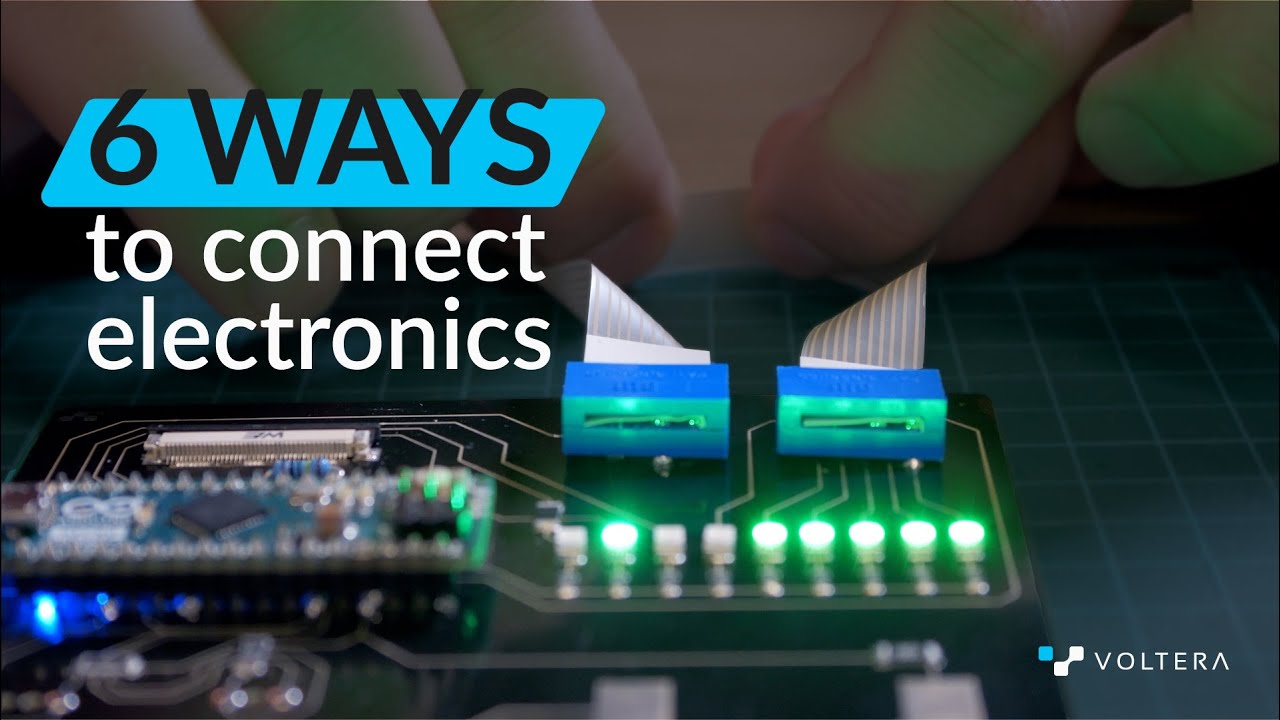
- Voltera: Connecting Flexible and Stretchable Substrates to Printed Circuit Boards
Connecting flexible circuits to traditional printed circuit boards (PCBs) is commonly called flexible-to-rigid interconnections. They enable flexible sensors, displays, wearables, and other flexible electronics to communicate with microcontrollers, power management systems, and external devices. MATERIALS USED NovaCentrix HPS-U11 silver nanoparticle ink ACI FS0142 flexible silver ink ACI SS1109 stretchable silver ink ACI SC1502 stretchable carbon ink ACI FC3203 flexible carbon ink VFP ECV003 UV-curable dielectric ink T4 Solder paste SUBSTRATES USED Polyethylene terephthalate (PET) Thermoplastic polyurethane (TPU) Polyimide (Kapton) 3" × 4" FR1 board TOOLS AND ACCESSORIES V-One PCB printer NOVA materials dispensing system Würth Elektronik 687140149022 FFC connector TE Connectivity AMP Connectors 487923-1 contact crimp pin connector Amphenol ICC (FCI) 66226-004LF 4 position FFC connector header CW Industries CWR-142-10-0203 IDC connector 3M electrically conductive adhesive transfer tape 9703 TLKKUE B0B1B33TZJ 10 mm snap connectors Guangshunle B0CXLL458K 15 mm snap connectors Arduino Micro controller We are Exhibiting in Berlin. Visit our booth at the TechBlick event on 22-23 October 2025 in Berlin . Contact us for your special discount coupon to attend Project overview Purpose The goal of this project was to validate five different ways of making reliable, accessible interconnections between flexible and rigid circuits — a common use case for a lot of our customers and essential to making flexible prototypes compatible with standard test equipment, breadboards, or rigid control systems. Design The project consisted of three parts: Printing the flexible circuits Capacitive touch sensor Force sensitive resistor (FSR) Flex sensor Strain gauge Ribbon cable Printing the rigid circuit Connecting flexible circuits to the rigid PCB using six types of commercially available connectors Zero insertion force (ZIF) connector Crimp connector Flexible flat cable (FFC) connector Snap connector Insulation displacement contact (IDC) connector Z-axis conductive tape Table 1 Connector Connected to Type Würth Elektronik 687140149022 FFC connector Capacitive touch sensor Rigid PCB ZIF Amphenol ICC (FCI) 66226-004LF 4 position FFC connector header Flex sensor Rigid PCB FFC TE Connectivity AMP Connectors 487923-1 contact crimp pin connector FSR Rigid PCB Crimp TLKKUE B0B1B33TZJ 10 mm snap connectors ECG electrodes Snap Guangshunle B0CXLL458K 15 mm snap connectors Heated mitten Snap CW Industries CWR-142-10-0203 IDC connector Ribbon cables Rigid PCB IDC 3M electrically conductive adhesive transfer tape 9703 Strain gauge Ribbon cable Rigid PCB Z-axis conductive tape Desired outcome Once the interconnections have been established, they should exhibit both mechanical fit and electrical integrity. To achieve that, each connector should fit snugly with no slippage or misalignment under normal handling and usage. In addition, the contact resistance should be low, effectively near-zero. Although we didn’t set metrics for measurements for the printed sensors, as a general rule, they should respond accurately to their respective physical inputs (pressure, strain, bending, capacitive touch) and maintain reliable electrical connections through repeated flexing or stretching. Functionality While all the methods we showcased are feasible for making interconnections, each of them offers different durability, reusability, and suits different applications. Table 2 Method Flexibility Reusability Notes ZIF Moderate Moderate to high Contact resistance ~25 mΩ-40 mΩ , durable up to 10k-20k insertion cycles Crimp Low High Reliable, rigid connection; ideal for bench setups FFC Moderate Moderate Used for flat, flexible cables; requires compatible locking connector Snap Moderate Moderate to high Good for removable modules; common in wearables IDC Low High Quick connections for ribbon/stretch cables Z-axis tape High Low to moderate Flexible; adhesive may degrade with repeated use. Many are single use only. The rigid PCB successfully helped us test the result of our interconnections, with total series resistance across each interconnection well below 1Ω, providing negligible signal loss. This aligns with common connector specifications and makes the connectors suitable for sensor interfacing. Printing the flexible circuits The flexible sensors were printed using the NOVA materials dispensing system with varying print settings. Printing the capacitive touch sensor This circuit consists of a touch electrode (large square pad at the top), and a trace leading down (and the small contact region at the bottom). Once printed and cured, the circuit was covered with Kapton tape to insulate and stabilize the touch interface. When a finger or conductive object approaches the pad, it increases the capacitance of that electrode relative to ground. Figure 1: Circuit design for the capacitive touch sensor Table 3 Ink ACI FS0142 flexible silver ink Substrate PET Print time 6 minutes 6 seconds Cure time and temperature 150°C for 15 minutes Figure 2: Printed capacitive touch sensor Printing the force sensitive resistor (FSR) This circuit consists of a piezoresistive element (red) as well as fine mottled traces (blue) that serve as interdigitated electrodes. When pressure is applied, the carbon film compresses and resistance drops between the interdigitated silver electrodes. Figure 3: Circuit design for the FSR Table 4 Ink ACI SS1109 stretchable silver ink (blue) ACI FC3203 flexible carbon ink (red) Substrate PET Print time 1 minutes 57 seconds (blue) 1 minutes 54 seconds (red) Cure time and temperature 135°C for 5 minutes (blue) 120°C for 15 minutes (red) Figure 4: Printed FSR sensor Printing the flex sensor This circuit consists of traces that form an electrically resistive sensing element (blue) as well as traces that form conductive interconnects (red). When the sensor bends, the carbon trace deforms, increasing its resistance. This resistance change is measured via the silver interconnect and used to quantify the degree of flex or curvature. Figure 5: Circuit design for the flex sensor Table 5 Ink ACI SS1109 stretchable silver ink (red) ACI SC1502 stretchable carbon ink (blue) Substrate PET Print time 1 minutes 51 seconds (red) 3 minutes (blue) Cure time and temperature 135°C for 5 minutes (red) 120°C for 15 minutes (blue) Figure 6: Printed flex sensor Printing the strain gauge and the ribbon cable The strain gauge and its interconnect were printed as two separate circuits: A serpentine resistive strain gauge (in red) A thin custom ribbon cable (in blue) acting as its signal extension The gauge’s silver pads were aligned with the ribbon cable’s contact pads and bonded using 3M anisotropic Z-axis conductive tape to ensure a solderless electrical connection. Figure 7: Circuit design for the strain gauge and ribbon cable Table 6 Ink ACI SC1502 stretchable carbon ink (red) ACI SS1109 stretchable silver ink (blue) Substrate TPU (red) Polyimide/Kapton (blue) Print time 19 minutes 19 seconds (red) 5 minutes 21 seconds (blue) Cure time and temperature 120°C for 15 minutes (red) 135°C for 5 minutes (blue) Figure 8: Printed strain gauge and ribbon cable Printing the ribbon cable The ribbon cable is a custom multi-conductor flat cable with parallel conducting traces evenly spaced, each one acting as an individual wire in the cable. The circular pads at each end are for electrical connection to the rigid circuit board with the IDC connectors. Figure 9: Circuit design for the ribbon cable Table 7 Ink ACI SS1109 stretchable silver ink Substrate TPU Print time ~ 13 minutes 28 seconds Cure time and temperature 135°C for 5 minutes Figure 10: Printed ribbon cables ECG sensors and heated mitten These flexible circuits were printed in previous applications and showcase the use case for snap connectors, which are ideal for wearable and textile-based electronics. Snap connectors are small, lightweight, and durable, making them perfect for applications that require repeated attachment and detachment, such as medical sensors and smart garments. They also provide a secure mechanical bond while maintaining user comfort and are easy to integrate into fabric or soft substrates. Check out the following white papers for details: Printing ECG Electrodes with Biocompatible Gold Ink on TPU Printing Silver Conductive Ink on Cotton Fabric Printing the rigid circuit This circuit was designed for integrating and testing flexible sensors and connectors. We first drilled through holes for the connectors. We then printed the circuit using the V-One PCB printer. The board routes signals from multiple connectors to a central microcontroller (Arduino Micro). Each sensor’s signal path includes passive components (e.g. resistors, capacitors), then branches to I/O pins and visual feedback via LEDs. Figure 11: Circuit design for the rigid PCB Table 8 Ink NovaCentrix HPS-U11 silver nanoparticle ink Substrate FR1 Nozzle type Voltera plastic nozzle Probe pitch 5 mm Print time 9 minutes 30 seconds Cure time and temperature 150°C for 30 minutes After curing the ink, we inserted copper rivets into the holes to provide robust physical anchoring. We then dispensed solder paste, placed the components onto the board, and ran a reflow cycle. Connecting flexible circuits to the PCB Figure 12: Printed sensors connected to the rigid board with different connectors Connecting the capacitive touch sensor This sensor was connected to the rigid PCB using a ZIF connector. We inserted the tail of the PET face-down (for bottom-contact) into the ZIF connector on the rigid PCB. We then closed the latch of the ZIF connector, clamping the tail in place. The advantages of this method includes: Low-profile, great for slim interfaces Non-permanent, easy replacement during prototyping No soldering required Stable contact for repeated use Figure 13: Connecting the capacitive touch sensor to the rigid board with the ZIF connector Connecting the force-sensitive resistor The connection to the rigid PCB is made using a crimp connector. The TE Connectivity AMP crimp pins were mechanically forced through the PET substrate at the silver contact pads. The crimping arms of each pin were then folded over and flattened tightly against the substrate to create a secure connection. Figure 14: Connecting the force sensitive resistor to the rigid board with the crimp connector This offers several advantages: Robust electrical connection Low-profile Reusable, ideal for prototyping and testing Connecting the flex sensor The flexible tail with silver pads was inserted into an Amphenol "clincher" FFC connector located on a rigid PCB. This connector clamps onto the pads, creating a secure, solder-free contact that relies on mechanical pressure to maintain electrical connectivity. That makes it non-destructive and reusable, ideal for testing and prototyping flexible sensors. Figure 15: Connecting the flex sensor to the rigid board with the FFC connector Connecting the strain gauge The Z-axis adhesive electrically connects the sensor pads of the strain gauge to the extension circuit and subsequently to the rigid board through vertical conduction only, preventing lateral shorts while also providing a low-profile, solderless bond. This makes it especially advantageous for heat-sensitive substrates like TPU or PET, where soldering could cause damage. The adhesive also eliminates the need for bulky connectors or reflow processes, ideal for fast assembly and prototyping. Figure 16: Connecting the strain gauge (and its flexible extension) to the rigid board with the Z-axis conductive tape Connecting the ribbon cable The connector pierces the substrate and makes contact with the conductive traces, allowing secure mechanical and electrical attachment. Figure 17: Connecting the custom ribbon cable to the rigid board with the IDC connector This offers several advantages: Seamless integration with no soldering or assembly needed Ultra-thin and lightweight compared to bundled wires. Customized length and pitch Handles movement and flex without mechanical strain on individual conductors Challenges and advice Reliability of Z-axis conductive tape Initial experiments with Z-axis conductive tape for component mounting revealed unreliable connections, especially under conditions of strain or flex. This tape is best suited for static or semi-flex applications, and applying sufficient vertical pressure is crucial to maintain good electrical contact. For more robust and permanent connections, especially in industrial applications, thermoset anisotropic conductive films are commonly used. Material selection and curing conditions During our initial testing, printing sensors with silver ink on PET frequently resulted in cracking. Adjustments included optimizing print thickness, selecting alternative inks (ACI SS1109, SC1502), and introducing dielectric layers as buffers to improve durability and resistance range. Conclusion By optimizing material choices, print parameters, and connector integration, we demonstrated reliable pathways for sensor signals. The five practical techniques — ZIF, crimp, snap, IDC, and Z-axis tape — each offer unique advantages for wearables, medical devices, and flexible prototypes. These solutions empower designers to overcome integration hurdles while maintaining signal integrity across dynamic interfaces. If you’re interested in our other projects involving the interface of flexible and rigid circuits, take a look at: Printing a Flexible Membrane Keyboard with Conductive Silver Ink and Dielectric Ink on PET Printing Strain Gauges on TPU laminated on a Glove for Remote Hand Control Printing a Flexible PCB with Silver Ink on PET Working with printed electronics and need help making interconnections? Book a meeting to speak with one of our technical representatives. We are Exhibiting in Berlin. Visit our booth at the TechBlick event on 22-23 October 2025 in Berlin Contact us for your special discount coupon to attend Download Conference Handout
- How Femtosecond Lasers are Advancing the Consumer Electronics Field
Deividas Andriukaitis (Main Author) [1], Paulius Gečys[2], Tadas Kildušis[3] [1] Ekspla, Vilnius, Lithuania | [2] Center for Physical Sciences and Technology, Vilnius, Lithuania | [3] Akoneer, Vilnius, Lithuania Contact: d.andriukaitis@ekspla.com , Deividas Andriukaitis The consumer electronics field continues to evolve rapidly, driven by tighter tolerances, higher quality, faster processing speeds, and novel functionalities. As manufacturing demands increase, femtosecond lasers have become an essential technology, playing a critical role in enabling these advancements. In this article, we explore how femtosecond lasers are shaping the development of consumer electronics and powering emerging manufacturing technologies. Figure 1. Fan-out circuit on PI. Courtesy of Akoneer Lasers have long contributed to technological progress across various domains - from telecommunications and metrology to automotive, semiconductor, and medical sectors. Among the different laser types, femtosecond lasers stand out due to their extremely short pulse duration (on the order of 10⁻¹⁵ seconds). When tightly focused, they enable highly localized energy delivery in both time and space, vaporizing material with minimal thermal effects - a process known as „cold“ ablation. Figure 2. Schematic of material processing with long and ultrashort pulse lasers. Courtesy of Amada Miyachi America Inc. To learn more about MicroLED and AR/VR displays please join the show in Eindhoven on 24 and 25 Sept 2025. Learn more [ here ] Thanks to this ultrashort energy deposition, femtosecond lasers can ablate materials before heat spreads into surrounding areas. Compared to nanosecond lasers, this results in superior processing quality, minimal heat-affected zones, and the ability to machine brittle or thermally sensitive materials such as polymers, ceramics, and metals. In many cases, the resulting quality is so high that no post-processing is needed, simplifying the overall production chain. Figure 3. Femtosecond laser FemtoLux 50. At Ekspla, we’ve been designing and manufacturing laser systems for over 30 years, with the mission of delivering reliable solutions for both scientific research and industrial applications. Our FemtoLux series of femtosecond lasers is widely used in micromachining tasks where precision and surface quality are essential. Through regular collaboration with customers, we've gathered a wide range of successful use cases that demonstrate the advantages of femtosecond laser processing. Glass, being transparent, brittle, and hard, is a natural fit for femtosecond laser processing. Applications include cutting, drilling, milling, scribing, dicing, and etching. One process gaining momentum is the creation of through-glass vias (TGVs) - narrow, deep holes in glass substrates used in advanced semiconductor packaging. A single glass interposer can contain thousands of these features, demanding a process that’s both reliable and scalable. Figure 4. TGV fabrication. (left) Selective laser etching of TGV, courtesy of WOP. (right, bottom) Percussion drilling of TGV, courtesy of Akoneer. Our FemtoLux 30 has proven effective for both ablation-based and selective laser etching approaches to TGV production, across materials such as Eagle XG and Borofloat 33. Its broad parameter tunability makes it well-suited for handling the material variability seen in different glass types, making it a strong candidate for high-precision glass micromachining tasks. Polymers pose a different challenge. Many are highly sensitive to heat, making it difficult to process them without damage. Femtosecond lasers, due to their minimal heat-affected zone, are ideal for this task. While most femtosecond lasers operate at 1030 nm, switching to shorter wavelengths can further reduce thermal effects. In one case, a customer working with a thermally sensitive polymer was dissatisfied with a 23 µm heat-affected zone at 1030 nm. By switching to the second harmonic (515 nm), absorption improved significantly, reducing the heat-affected zone to just 8 µm - well within the required tolerances. Figure 5. Processing of polyimide with femtosecond laser operating at wavelength of 515 nm. Femtosecond lasers also excel in metal micromachining, offering burr-free edges and negligible heat-affected zones. This enables the production of intricate metal parts without the need for secondary operations. We’ve successfully demonstrated processing on stainless steel, aluminum, copper, brass, and nitinol, as well as multilayer foils used in battery and energy storage applications. Figure 6. Processing of stainless-steel with femtosecond laser. Beyond material removal, femtosecond lasers are unlocking new possibilities in additive manufacturing and electronics fabrication. One standout example is Selective Surface Activation Induced by Laser (SSAIL) - a laser-based metallization method to complement or replace traditional photolithography. While photolithography offers high resolution, it comes with significant cost and complexity. Meanwhile, additive methods like inkjet printing offer flexibility but are often limited in speed and scalability. SSAIL addresses this gap by enabling the creation of copper traces with resolutions down to 1 µm and throughput comparable to lithography - while maintaining the simplicity and digital control of additive approaches. The process begins with laser modification, where an ultrashort pulse laser selectively alters the substrate’s surface, introducing microscale structural and chemical changes. These modified regions are then subjected to catalytic activation by immersion in a metal precursor solution, which binds selectively to the laser-processed areas. Finally, an electroless plating process deposits a uniform copper layer only on the activated regions, resulting in precise and conductive traces. With its combination of resolution, speed, and simplicity, SSAIL presents a strong case as a next-generation technology for electronics manufacturing. Figure 7. SSAIL process steps for micro trace formation, courtesy of Akoneer. To learn more about MicroLED and AR/VR displays please join the show in Eindhoven on 24 and 25 Sept 2025. Learn more [ here ] Femtosecond lasers are already playing a crucial role in advancing the consumer electronics field by enabling high-precision, high-quality processing of a wide range of materials. As demand grows for tighter tolerances, smaller features, and more efficient production methods, the importance of ultrafast laser technologies will only increase. With ongoing improvements in performance and integration, femtosecond lasers are set to become an even more central tool in developing next-generation electronic devices. At Ekspla, our FemtoLux line of femtosecond lasers is well-positioned to support this progress - offering the flexibility, reliability, and precision needed to meet the challenges of tomorrow’s manufacturing. Figure 8. Fan-out circuit demo on glass material fabricated using SSAIL technology, courtesy of Akoneer.
- Introducing the Program - Smart surfaces and sensors
Why Should You Join TechBlick's The Future of Electronics RESHAPED? The Future of Electronics RESHAPED conference and exhibition (22 & 23 OCT 2025, Berlin) is set to be the most important event of the year focused on additive, hybrid, 3D, sustainable, wearable, soft and textile electronics. This year the program features a world-class agenda with over 100 superb invited talks from around the world, 12 industry- or expert-led masterclasses, 4 tours, and over 90 onsite exhibitors. In this article, we discuss and highlight various innovative talks at the event around the theme of smart surfaces and sensors. In future articles, we will cover further technologies including smart surfaces, sustainable electronics, printed medical electronics, novel materials and beyond. Explore the full agenda now and join the global industry in Berlin on 22 & 23 OCT 2025. Let us RESHAPE the Future of Electronics together, making it Additive, Hybrid, 3D, R2R, Soft, Flexible, Wearable, Textile and Sustainable. 🚨Register before 12 September to save 200 Euros on top of early bird discounts. This is a one-time offer. The coupon can be obtained here🚨 Toyota – Michael Rowe presents technology opportunities beyond automotive , showcasing cross-industry applications of actuator, sensor, and material innovations. Highlights include shape memory alloy (SMA) wire actuators delivering lightweight, translational motion with integrated feedback; near-IR reflective pigments enabling hidden data transfer for autonomous systems; and metamaterial-based vibration dampening for electronic housings. Auburn University – Pradeep Lall explores additively printed in-mold electronics (IME) circuits and sensors as a lightweight alternative to traditional wire harnesses in vehicles. Using direct-write and gravure offset printing on thermoformed substrates such as PETG, PC, and HIPS, Auburn demonstrates multilayer circuits with mounted components and electrodermal sensors. Applications include driver monitoring, ADAS integration, and signal processing, with results showing performance parity with conventional rigid circuits. Trusscore – Chad Smithson presents electrochromic wall panels for on-demand color change . Using multilayer printed films integrated onto rigid PVC, the panels shift color via a reversible redox reaction under <3 V bias, ensuring low power draw and safety. The talk covers scaling from lab to production, challenges in ink selection, device architecture, and compatibility of print sequences. 🚨Register before 12 September to save 200 Euros on top of early bird discounts. This is a one-time offer. The coupon can be obtained here🚨 Antolin – Stephan Horn discusses dynamic automotive interiors using electronic ink . In collaboration with E Ink, Antolin integrates Prism™ technology into interior trim, enabling surfaces that change color and patterns on demand or in response to alerts. The technology consumes energy only during transitions, enhancing efficiency and driving range. Automotive prototypes demonstrate validated performance under real-use conditions. ruhlamat – Michael Bruns explores embedded wire technologies for 3D-formed electronics and smart surfaces . Techniques such as in-mold wire embedding, additive manufacturing, and thermoforming-compatible conductive traces enable robust interconnections in curved geometries. Applications include automotive and consumer products, where 3D wiring enhances ergonomics, user interfaces, and sensor integration, pointing toward multifunctional smart skins and hybrid printed–wire electronics. Valeo – Martial Berry presents introducing printed and in-mold electronics into automotive products . The talk outlines Valeo’s structured approach to integrating new technologies under strict performance and quality demands, covering development timelines, resources, and specifications needed to bring printed and IME solutions into next-generation vehicles. Explore the Full Agenda and Register before 12 September 2025 for the best rates CurveSYS Sensors – Denis Guezelocak presents smart conformal pressure-sensitive sensors for security fields . Flexible sensor arrays with multi-zone architectures enable real-time impact detection and differentiation between low-force events and high-energy strikes or ballistic impacts. Coupled with data fusion and intelligent signal processing, the technology enhances situational awareness and response capabilities in security and defense applications. iGii – Michelle Ntola discusses 3D carbon nanomaterials (Gii™) for sensing and diagnostics . With high surface area, porosity, and biocompatibility, these nanocarbon frameworks enhance electrochemical signal transduction, multiplexed detection, and low non-specific adsorption. Roll-to-roll, low-temperature processes enable cost-effective point-of-care devices, with applications extending to catalysis, energy storage, and heating. Armor Smart Films – Fabien Resweber showcases functionalized surfaces using advanced coatings and electroactive polymers . Leveraging P(VDF-TrFE) piezoelectric materials, Armor enables scalable production of next-generation sensors, haptic interfaces, heating films, and medical devices. The focus is on flexible, efficient, and seamlessly integrated functional surfaces for industrial and healthcare applications. NGK Europe GmbH – Daniel Harden presents ultra-thin, semi-solid-state Li-ion batteries with ceramic electrodes for wearables and IoT. The design minimizes liquid electrolyte and eliminates binders, enhancing safety, thermal stability, and fast charging while enabling reliable integration with energy-harvesting systems for long-life autonomous devices. 🚨Register before 12 September to save 200 Euros on top of early bird discounts. This is a one-time offer. The coupon can be obtained here🚨
- Full Program: The Future of Electronics RESHAPED Berlin
22 & 24 October 2025 | ECC, Berlin | Conference & Exhibition This is the must-attend event of the year , focusing on additive, printed, 3D sustainable, wearable, flexible, hybrid, soft, stretchable, textile, structural and R2R electronics. This year the event will feature: ✅ 100+ speakers ✅ 90+ exhibitors showcasing all the key innovations ✅ 12 expert- and industry-led masterclasses ✅ 3 guided tours ✅ Networking with 600+ global participants ✅ Annual access to all TechBlick online events, on-demand version of all onsite events, as well as an on-demand library featuring over 1500 talks and masterclasses. 🚨Register before 12 September to save 200 Euros on top of early bird discounts. This is a one-time offer. The coupon can be obtained here🚨 Explore The Agenda See the most up-to-date conference agenda here 22 October | Conference Day 1 Track 1 09:00 | TechBlick | Welcome & Introduction 09:10 | Toyota | Technology Opportunities That Go Beyond Automotive 09:30 | Fuji Corporation | Additively manufactured multi-layer and stacked circuits with embedded electronics components 09:50 | Lockheed Martin | Flexible Hybrid Electronics in the Wild: How Copper Printing and Flexible RF Circuits Made it Out of the Lab and Into the Field 10:10 | NanoPrintek | Inkless Multimaterial Printing Directly from Raw Materials - Breaking the Barriers in Cost, Time, Pollution, and Supply Chain Networking Break 11:15 | University of Rome Tor Vergata | Scalable and Ambient-Air Processing of Printed Perovskite PV Modules 11:35 | CubicPV | Enabling Durable Perovskite Tandems with Scalable Architecture and Manufacturing Methods 11:55 | Solaires Entreprises Inc | From Lab to Fab: Navigating the Challenges and Lessons Learned in Scaling Perovskite PV Modules 12:15 | Institut Photovoltaïque d'Île-de-France (IPVF) | From Lab to Fab: Navigating the Challenges and Lessons Learned in Scaling Perovskite PV Modules Lunch & Exhibition Break 14:05 | SATO Global | How digital twins support Industry 4.0 and what comes next in RFID 14:25 | Wiliot | Scaling Ambient IoT: Wiliot’s Battery-Free Bluetooth Revolution with Printed Sensing and Reel-to-Reel Manufacturing Technology 14:45 | Sunray Scientific Inc | Ultraviolet Light-Cured Anisotropic Conductive Epoxy for Low Cost, High Throughput Electronic Assemblies 15:05 | University of Glasgow | Sustainable Wireless Battery-Free and Chip-Free Sensors and IDs Exhibition & Refreshment Break 16:10 | Essemtec | Jetting and SMT mounting technologies for additive and printed electronics on flexible and stretchable substrates 16:30 | VTT | Flexible hybrid multi-layer complex systems: Prototyping and Process Development 16:50 | Fraunhofer ENAS | Ultra-thin Parylene-based Printed Circuit Boards for the next generation of flexible electronics 17:10 | TracXon | Expanding the boundaries of printed electronics for volume manufacturing of PCB-replacements Drinks Reception Track 2 09:10 | Oxford PV | The world's first commercial tandem perovskite-silicon module 09:30 | Hangzhou Microquanta Semiconductor | Bridging the Gap: The Commercial Readiness of Perovskite PV 09:50 | Swift Solar | Unlocking the Potential of Perovskite-Silicon Tandem PV: Insights into the Journey from Lab to Fab 10:10 | Solar and Renewable Industry Leader | The Future of European and U.S. Solar Manufacturing: Niche Only or Mass Production? Exhibition & Refreshment Break 11:15 | Würth Elektronik GmbH & Co. KG | Towards Sustainable PCBs: Design, Process Efficiency and Material Innovation for a Greener Lifecycle 11:35 | Signify Research | Printed Electronics, an opportunity for lighting? 11:55 | Dresden Integrated Center for Applied Physics and Photonic Materials - TU Dresden | Leaftronics: novel devices based on leaf skeletons 12:15 | Holst Centre | Recyclability of In-Mold Electronics Lunch & Exhibition Break 14:05 | Q5D | 5 axis laser-assisted selective metallization of large 3D parts 14:25 | XTPL | Additive Manufacturing for Next-Generation Microelectronics 14:45 | AMAREA Technology | Ceramic-Based Printed Electronics Enabled by Multi-Material Additive Manufacturing 15:05 | Lithoz | Additive Manufacturing of Dielectric Ceramics and Ceramic–Metal Components Using Lithography-Based Ceramic Manufacturing Exhibition & Refreshment Break 16:10 | Henkel | High Performance Inks for Cost Efficient Manufacturing of Printed Electronics 16:30 | CondAlign | Novel conductive films – from launch to volume production 16:50 | University of Coimbra | Scalable, High-Resolution Microchip-Integrated Liquid Metal Circuits: Enabling the Next Generation of 3R Electronics 17:10 | The University of Manchester | Graphene and 2D materials printed electronics Drinks Reception Track 3 11:15 | CurveSYS Sensors | Smart Sensors for Security Fields 11:35 | Heraeus Electronics | Bridging the Gap Between Additive and Subtractive Technologies: the Solderable Polymer Revolution 11:55 | Blackleaf | Graphene-based Electric Heating: how graphene films are reinventing surface heating in the industry 12:15 | ELANTAS Europe GmbH | Printed Electronics in the fast lane: Paste technologies driving tomorrow’s mobility Lunch & Exhibition Break 14:05 | iGii | Revolutionising sensing and diagnostics with 3D carbon nanomaterials 14:25 | NGK Europe GmbH | [TBC] 14:45 | Armor Smart Films | Armor Smart Films: Empowering Scalable Innovation in Functional Surfaces 15:05 | RISE | Screen printed stretchable electronics including liquid metals Exhibition & Refreshment Break 16:30 | TNO partner in Solliance | Pioneering Perovskite Scalability: Advancing Roll-to-Roll Slot Die Coating for Stable and Efficient Flexible Solar Cells 16:50 | Heliatek | Certified, flexible and lightweight PV modules on a commercial scale 17:10 | OET Energy Technologies | Scaling Printed Photovoltaics: From 3rd Gen PV Innovation to Giga Fab Industrialization Drinks Reception Track 4 11:15 | National Research Council Canada | 3D electronics with volumetric additive manufacturing 11:35 | Notion Systems | New products for development and scale-up of functional inkjet processes to industrial production 11:55 | ImageXpert | Selecting the Right Inkjet Printhead for Advanced Electronics Applications 12:15 | Printed Electronics Limited | Drop-on-Demand Printing of Highly Viscous Inks Lunch & Exhibition Break 14:05 | Sofab Inks | Novel materials for next-generation perovskite solar panel production processes 14:25 | Karlsruhe Institute of Technology | New Materials for Metallization and Interconnection of Perovskite Reduced Silver Consumption 14:45 | Nano-C, Inc. | Innovative Interface Materials for Perovskite Photovoltaics 15:05 | DELO Industrial Adhesives | Pioneering the Future: DELO's Advanced Adhesives Enhance Perovskite Solar Cell Protection Exhibition & Refreshment Break 🚨Register before 13 September to save 200 Euros on top of early bird discount. This is a one-time offer. The coupon can be obtained here🚨 23 October | Conference Day 2 Track 1 09:10 | Valeo | Introducing new technologies into automotive products: Valeo’s path with Printed and In-Mold Electronics 09:30 | Auburn University | Additively Printed In-Mold Electronics Circuits and Sensors for Automotive 09:50 | GE Aerospace | Additive Electronics for Harsh Environment Applications in Aerospace 10:10 | NextFlex | Commercialization of Additively Manufactured Electronics Exhibition & Refreshment Break 11:15 | Fraunhofer ISE | Sustainable Fabrication of Perovskite Modules: Strategies for scalable devices with low material criticality 11:35 | SparkNano | On a Roll: Spatial ALD Advances Scalable Perovskite Solar Manufacturing 11:55 | AeroSolar | Aerosol treatment of perovskite solar cells for improved efficiency, stability and manufacturing yield Lunch & Exhibition Break 13:15 | HighLine Technologies | Scalable Solutions, from Microextrusion to Coating 13:35 | Ceradrop - MGI Digital Technology | [Title TBC] 13:55 | Sonojet | SAW-Based Aerosol Printing for the Future of Electronics 14:15 | Enjet | Redefining Functional Printing: Innovations in EHD Inkjet Multi-Nozzle Technology Exhibition & Refreshment Break 15:05 | X-Fab | Micro-Transfer Printing: Integrate ultra-thin ASICs to enable sophisticated Applications 15:25 | Mesoline | Microchannel particle deposition for MEMS & Sensors Applications 15:45 | Prio Optics GmbH | Precision Through Additive Manufacturing: Inkjet-Printed Optical Coatings Track 2 09:10 | Caelux Corporation | Meeting Future Energy Needs With High Density Solar 09:30 | Helmholtz-Zentrum Berlin | [Title TBC] 09:50 | Perovskia Solar | Charged by Light – Designed for Life 10:10 | CEA | Challenges for upscaling Perovskite/Silicon tandem solar cells Exhibition & Refreshment Break 11:15 | Fraunhofer EMFT | Endless electronics by R2R processing 11:35 | Eastman Kodak | Flexo for High-Resolution Roll-to-Roll Manufacturing 11:55 | LightnTec | [Title TBC]. Lunch & Exhibition Break 13:15 | Fraunhofer ILT | Optimizing Local Conductivity in Printed Electronics: A Laser-Controlled Approach 13:35 | Hamamatsu | Leveraging Laser Processing for Sustainable Printed Electronics – Laser Sintering, Encapsulation & Soldering 14:05 | Akoneer | Making of multilayer glass HDI PCB 14:15 | DR Utilight Corp | Laser Pattern Transfer Printing for High-Viscosity Pastes Exhibition & Refreshment Break 15:05 | Smartkem | OTFT circuit developments enabling low-voltage flexible processors 15:25 | Canatu | ADAS camera heaters, advancing autonomous driving in any weather 15:45 | INKTIO | From Ink to Impact: Digital Manufacturing of Flexible Photocatalytic Electronics Track 3 11:15 | Hummink | HPCaP (High Precision Capillary Printing): A Technology for Next-Generation Manufacturing 11:35 | Suss MicroTec | Pushing the Limits of Inkjet Printing: A Flexible Platform for Micro- and Multi-Material Deposition 11:55 | Myrias Optics + UMass Amherst | Printed Metaoptics for AR/VR and Photonics Lunch & Exhibition Break 13:15 | INO d.o.o. | From R&D to high volume production and importance of modular equipment 13:35 | Conductive Technologies | Engineering Functionality: Material Strategies for Modern Sensors 14:15 | Panasonic | Multifunctional Shock Absorb Film Material, Toughtelon Exhibition & Refreshment Break 15:05 | SOLRA-PV | The Industrialization of Perovskite-Based Indoor Photovoltaics 15:25 | P3C Technology and Solutions Pvt Ltd | Scaling Perovskite Solar Module Technology in India: Field Deployment and Commercialization Roadmap Track 4 11:15 | Antolin | Automotive interiors dynamic decoration with electronic ink 11:35 | Trusscore | Changing your wall colour on demand using electrochromics 11:55 | ruhlamat GmbH | Embedded wires for 3D formed electronics and smart surfaces Lunch & Exhibition Break 13:15 | SOLRA-PV | The Industrialization of Perovskite-Based Indoor Photovoltaics 13:35 | SALD B.V. | A Paradigm Shift in Roll-to-Roll Spatial Atomic Layer Deposition for Perovskite Solar Cell Manufacture 14:15 | Panacol-Elosol GmbH | Advanced Bonding Technologies for Flexible Substrates and Electronic Devices 14:35 | Intellivation LLC | R2R Laser Processing of Multi-Layer Vacuum deposited coatings on flexible substrates for 2D Functional Devices 🚨Register before 12 September to save 200 Euros on top of early bird discount. This is a one-time offer. The coupon can be obtained here Masterclasses and Tours Explore our masterclass and tour program here. Masterclasses | Track 1 (21 OCT 2025) 09:00 | Nagase ChemteX | Selecting Conductive Inks: A Property-Driven Approach for Printed Electronics Applications 10:00 | Heraeus Electronics | Printable Thick Film Heaters: Essentials for Design, Material Selection, and Printing 11:00 | Fraunhofer IFAM | Screen Printing Technology For Printed Electronics Manufacturing 12:00 | 3E Smart Solutions / ZSK | Driving Reliability and Scalability in E-Textiles and Wearables via Embroidery Technologies | Chip Interconnections for Flexible Printed Electronics. Masterclasses | Track 2 (21 OCT 2025) 09:00 | Hahn-Schickard | Multi-material Additive Manufacturing of 3D Electronics 10:00 | Voltera | Advancements in Printed Electronics Prototyping: Direct Ink Write Technology for Printed Multi-Layer Flexible Electronics 11:00 | Silicon Austria Labs GmbH | Life Cycle Assessment of Printed Electronics: Challenges, Insights and Opportunities 12:00 | CEA | Advancing PCB Technology Through Additive Manufacturing: Process, Sustainability, and Reliability Masterclasses | Track 3 (21 OCT 2025) 09:00 | imec | Stable and efficient architectures for perovskite solar modules and tandems 10:00 | Swansea University | Printing Perovskite Solar Modules using S2S and R2R processes 11:00 | Coatema | Slot Die Coating: Principles and Practice Towards Mass Production 12:00 | Fraunhofer IAP | Towards Non-Toxic and Sustainable Materials in Perovskite Photovoltaics Tours to: Fraunhofer IAP, Fraunhofer IZM, Helmholz Zentrum Berlin/PVcomB 🚨Register before 12 September to save 200 Euro on top of early bird discounts. This is a one-time offer. The coupon can be obtained here Exhibition Explore the exhibition floor here 🚨Register before 12 September to save 200 Euro on top of early bird discounts. This is a one-time offer. The coupon can be obtained here🚨 Gold Exhibitors Dimension Division Heraeus Electronics Henkel Nagase ChemteX Notion Systems Silver and Standard Exhibitors ACI Materials Akoneer Ames Goldsmith Armor Smart Films Blackleaf Ceradrop - MGI Digital Technology Coatema CondAlign Conductive Technologies Creative Materials Inc. Delo Eastman Kodak Company ELANTAS Europe GmbH Ercon Fuji Corporation Hamamatsu HighLine Technology Holst Centre Hummink ImageXpert INO, d.o.o., Žiri Integrated Graphene (iGii) Intellivation LLC Kimoto Linxens Nano-C NanoPrintek NGK Europe GmbH NovaCentrix OET Energy Technologies & Coatema Panacol Panasonic Electronic Materials Policrom Printed Electronics Limited Smartkem SparkNano SPGPrints Sun Chemical SunRay Scientific SUSS The University Of Manchester TracXon Voltera VTT XTPL ABeetle Corporation Agfa Ail Arian Alpha Precision Systems (APS) Arkema Beespenser BrightSpot Automation LLC Brilliant Matters CEA Chimet S.p.A Coveme Spa DoMicro BV droptical GmbH FOM Technologies Fraunhofer IAP Fraunhofer IFAM Grafisk Maskinfabrik A/S GraphEnergyTech IPVF Joanneum Research JP Kummer Semiconductor Technology GmbH National Research Council Canada Noctiluca Normandy Coating nsm Norbert Schläfli AG PINA CREATION Polytec GmbH PrintUp Institute PROFACTOR GmbH PROTEX INTERNATIONAL RK Siebdrucktechnik RISE ruhlamat Silicon Austria Labs GmbH Sofab Inks Inc. Solaveni Technic, Inc. THIEME Toray Research Center, Inc. VFP Ink Technologies 🚨Register before 12 September to save 200 Euro on top of early bird . This is a one-time offer. The coupon can be obtained here🚨
- Introducing the Program - Additive and 3D Electronics Manufacturing Process Innovation
Why Should You Join TechBlick's The Future of Electronics RESHAPED? The Future of Electronics RESHAPED conference and exhibition (22 & 23 OCT 2025, Berlin) is set to be the most important event of the year focused on additive, hybrid, 3D, sustainable, wearable, soft and textile electronics. This year the program features a world-class agenda with over 100 superb invited talks from around the world, 12 industry- or expert-led masterclasses, 4 tours, and over 90 onsite exhibitors. In this article, we discuss and highlight various innovative talks at the event around the theme of Additive and 3D Electronics Manufacturing Process Innovation. In future articles, we will cover further technologies including smart surfaces, sustainable electronics, printed medical electronics, novel materials and beyond. In previous articles we introduced other innovations in Additive and 3D electronics (see here ) and also key material related innovations which will be showcased at the show (see here ) Explore the full agenda now and join the global industry in Berlin on 22 & 23 OCT 2025. Let us RESHAPE the Future of Electronics together, making it Additive, Hybrid, 3D, R2R, Soft, Flexible, Wearable, Textile and Sustainable. Explore the Full Agenda and Register before 12 September 2025 for the best rates GE Aerospace – Felippe Pavinatto presents additive electronics for aerospace applications in harsh environments . Examples include direct-write 3D printed passive RF sensors operating up to 1000 °C and fully additive embedded die packaging. Both demonstrate how additive methods enable non-planar, embedded devices beyond the limits of conventional semiconductor manufacturing. Mesoline – Thomas Russell presents microchannel particle deposition (MPD) for MEMS and sensor applications . This wafer-scale technology enables micron-precision material deposition on 6- and 8-inch wafers. Demonstrated use cases include uniform low-power gas sensors, high-resolution glass frit bonding lines (~20 µm), and high-aspect-ratio hydrogen getters on CMOS wafers, advancing device miniaturization and performance. Prio Optics – Dr. Qihao Jin presents inkjet-printed optical coatings for precision photonics . Functional inks are deposited with nanoscale accuracy to tune layer thickness, refractive index, and patterns for applications such as anti-reflective layers, spectral filters, and optical intensity control. Compared to vacuum deposition, the additive process reduces waste, accelerates prototyping, and scales from small to large-area optics for imaging, displays, sensors, and solar control. X-Fab – Tino Jaeger presents micro-transfer printing for integrating ultra-thin ASICs . The technology enables precise, high-throughput transfer of free-standing chiplets from CMOS and III-V wafers onto flexible foils and other substrates. The talk covers CMOS post-processing flows, tether/anchor structures, and heterogeneous integration approaches, highlighting applications where ultra-thin chiplets unlock advanced functionality. Explore the Full Agenda and Register before 12 September 2025 for the best rates Enjet – Doyoung Byun presents innovations in electrohydrodynamic (EHD) inkjet multi-nozzle printing . The talk outlines advances that overcome electrical crosstalk and interference, enabling stable, high-throughput jetting of viscous functional materials with micron precision. This scalable architecture positions EHD printing as a key technology for next-generation semiconductors, displays, and bioelectronics. Sonojet – Mehrzad Roudini presents SAW-based aerosol printing for next-generation electronics . Using surface acoustic waves on piezoelectric chips, this solid-state, nozzle-free approach enables low-power, tunable droplet generation from submicron to tens of microns. Integrated with on-chip microfluidics, the compact printheads are clog-free, compatible with a wide range of inks, and offer precise, energy-efficient deposition for high-resolution, multi-material additive manufacturing. HighLine Technologies – Maximilian Pospischil presents scalable deposition solutions from microextrusion to coating . The company’s high-speed dispensing achieves homogeneous fine lines below 20 µm at >500 mm/s, with expanded capabilities for cathode layer coating and other applications. Modular nozzle kits, multi-head systems, and AI-driven process optimization enable flexible, automated solutions for PV metallization and large-scale manufacturing. Explore the Full Agenda and Register before 12 September 2025 for the best rates Fraunhofer ILT – Adam El-Sarout presents laser-controlled optimization of local conductivity in printed electronics . The approach uses selective laser sintering to correct printing-induced conductivity variations in thin silver layers, achieving resistance fluctuations below 1 Ω. This two-step process enhances the performance and reliability of digitally printed strain gage sensors, offering a cost-efficient alternative to conventional lithography. NanoPrintek – Masoud Mahjouri-Samani presents inkless multimaterial printing directly from raw materials . This dry-printing process bypasses costly ink formulation and post-processing, generating pure nanoparticles in situ and sintering them with lasers onto diverse substrates. Capable of printing metals, semiconductors, insulators, and composites, the approach reduces cost, pollution, and supply-chain dependence while enabling hybrid, multifunctional structures for electronics, energy, healthcare, and aerospace applications. Akoneer – Tadas Kildušis presents multilayer glass HDI PCBs enabled by laser processing . Glass substrates offer advantages for electronics and semiconductor packaging, and Akoneer demonstrates methods for creating high-density interconnections in multilayer glass PCBs using advanced laser technologies. Hamamatsu – Alexander Görk presents laser processing for sustainable printed electronics . The talk highlights energy-efficient laser sintering, encapsulation, and soldering of NIR-absorbing materials, demonstrating how laser thermal processing supports greener materials and sustainable manufacturing through collaborations with material suppliers, institutes, and integrators. Explore the Full Agenda and Register before 12 September 2025 for the best rates Myrias Optics & University of Massachusetts Amherst – James Watkins present printed metaoptics for AR/VR and photonics . Using additive nanoimprint lithography with nanoparticle inks, wafer-scale fabrication of inorganic metalenses, metasurfaces, and AR/VR waveguides is demonstrated, achieving >80% efficiency and excellent uniformity. The process enables high-index, stable, and low-cost optical devices, paving the way for scalable integration of metaoptics on glass and silicon platforms. Hummink – Elisa Duquet presents High Precision Capillary Printing (HPCaP) for next-generation manufacturing . Inspired by AFM, HPCaP uses capillary forces and resonant micropipettes to achieve resolutions from 50 µm down to 100 nm without external energy input. Capable of depositing polymers, conductive inks, and biomaterials—including high-viscosity formulations—it enables high-aspect-ratio structures and fine interconnects for applications in semiconductor packaging, display repair, biosensors, and precision devices. Fuji Corporation – Ryojiro Tominaga presents additively manufactured multilayer and stacked circuits with embedded components . Using inkjet-printed silver nano-inks on UV-curable resin substrates combined with ultra-low temperature SMT, Fuji demonstrates 3D encapsulated devices with novel geometries. This approach highlights the potential of additive manufacturing to transform electronic device design and production. Explore the Full Agenda and Register before 12 September 2025 for the best rates
- MicroLED & AR/VR Display Innovations: Mass Transfer, Wafer Metrology, Red GaN, Perovskite QDs, Smart Glasses, and Scalable Manufacturing
We cover these points by sharing short (1min or so) handpicked snippets from their live recent talks at TechBlick and MicroLED Connect conferences and exhibitions In this newsletter we cover the following MicroLED Wafer Metrology and Calibration Strategies Assessing the Practicality of MicroLED Displays for Mass Production Stamp-Based Imprinting for AR Waveguide Manufacturing Advances in Mass Transfer Processes for MicroLED Chip Integration VR vs. AR: Market Outlook and Growth Limitations Perovskite Quantum Dots for High-Density Color Conversion Challenges and Advances in Native Red MicroLED Efficiency Etching and Deposition Solutions for MicroLED Materials Progress Toward Emissive Quantum Dot–EL Displays Cubic GaN as a Novel Platform for Scalable MicroLEDs Wafer-to-Wafer Integration for MicroLED Microdisplays MicroLED Smart Glasses and Market Update for AR Applications Integrated Production Platforms for Scalable MicroLED Manufacturing Join the MicroLED Connect + AR/VR Connect 2025 on 24 & 25 Sept 2025 at the High Tech Campus in Eindhoven (Netherlands). Explore full agenda here and register before 12 Sept when the FINAL early bird rates expire https://www.microledconnect.com/ https://www.microledconnect.com Manufacturing Processes & Integration Advances in Mass Transfer Processes for MicroLED Chip Integration Mass transfer remains one of the biggest hurdles for cost-effective microLED displays. At MicroLED-Connect 2024, Toray Engineering presented a new transfer method combining microLED chips with a panel-level package. Stamp-Based Imprinting for AR Waveguide Manufacturing Waveguides are key for AR devices, but must balance cost and performance. At Display Innovation Day (Dec 2024), SCIL presented its stamp-based system for waveguide imprinting as a scalable solution. Wafer-to-Wafer Integration for MicroLED Microdisplays Wafer-to-wafer processes are emerging as the path to mass production of microLED microdisplays. At MicroLED-Connect 2024, MICLEDI (imec spin-out) detailed its 300 mm CMOS integration flow and why wafer-level integration is critical. Integrated Production Platforms for Scalable MicroLED Manufacturing At MicroLED-Connect 2024, VueReal presented its platform for scalable microLED display production, addressing key challenges in cost, yield, and throughput. Materials Innovations Challenges and Advances in Native Red MicroLED Efficiency Native red microLEDs remain a bottleneck for performance. At MicroLED-Connect 2024, UCSB’s Prof. DenBaars presented the latest advances in tunnel-junction technology and efficiency gains versus OLED benchmarks. Etching and Deposition Solutions for MicroLED Materials Oxford Instruments shared processing solutions for GaN and InGaAlP materials, including AlInGaP etching and ALD-based passivation. Perovskite Quantum Dots for High-Density Color Conversion CEA-Leti’s Prof. François Templier presented research on perovskite quantum dots achieving sub-micron densities for color conversion in microLED displays. Progress Toward Emissive Quantum Dot–EL Displays QNA Technology updated on progress towards QD-EL displays, sharing the latest status of emissive quantum dot research and scalability. Cubic GaN as a Novel Platform for Scalable MicroLEDs Kubos Semiconductors detailed its cubic GaN material system, showing how it can enable efficient, scalable microLED manufacturing. https://www.microledconnect.com Metrology, Testing & Inspection MicroLED Wafer Metrology and Calibration Strategies MicroLED displays remain at an early stage, making precise optical measurement and wafer inspection critical for success. In our Display Innovation Webinar (Dec 2024), Tobias Steinel (Instrument Systems) introduced PL and EL test strategies, and highlighted how calibration reduces errors and improves performance in mass production. https://www.microledconnect.com Applications & Market Outlook Assessing the Practicality of MicroLED Displays for Mass Production Mikro Mesa presented key considerations around microLED driving, power consumption, and production readiness at MicroLED-Connect 2024. VR vs. AR: Market Outlook and Growth Limitations Yole Group’s Raphaël Mermet-Lyaudoz explained why VR may face a growth ceiling while AR has stronger market potential. MicroLED Smart Glasses and Market Update for AR Applications Omdia provided a market update on microLED adoption in AR smart glasses, highlighting recent product launches with full-color microLED solutions.
- Scalable Metal Oxide Nano Inks for High-Performance Organic, Perovskite, and Thin Film Photovoltaics and OLEDs
#PerovskiteSolarCells #OLED #OrganicPV #PrintedElectronics #NanoInks #ElectronTransportLayer #FlexibleElectronics #Optoelectronics #RollToRoll #SmartMaterials #EnergyTech #SolarInnovation #DisplayTechnology #NextGenMaterials #SustainableElectronics Author: Maryam Bari & Ashwani Jain PINA CREATION Unlocking printable, low-temperature charge transport layers for next-generation optoelectronics As next-generation optoelectronic technologies—such as Perovskite solar cells (PSCs), OLED displays, and Organic photovoltaics (OPVs) —move from lab to large-scale manufacturing, the pressure is on to find materials that are not only high-performing, but scalable, stable, and compatible with printed device architectures . A critical bottleneck remains the Electron Transport Layer (ETL) and Hole Transport Layer (HTL) . For technologies relying on delicate or flexible substrates, traditional materials such as Organic Semiconductors and traditional metal oxide inks pose serious limitations. High-temperature processing, moisture sensitivity, high cost, and limited lifetime all threaten the viability of commercial deployment. At PINA Creation , we’ve developed a line of ready-to-use SnO₂, NiO and ZnO nano inks that overcome these barriers and unlock practical, large-area fabrication for flexible and rigid optoelectronics. We are Exhibiting in Berlin. Visit our booth at the TechBlick Perovskite Connect event co-located with the Future of Electronics RESHAPED on 22-23 October 2025 in Berlin . Contact us for your special discount coupon to attend The ETL & HTL Processability The ETL & HTL are responsible for: Extracting electrons (ETL) and hole (HTL) from the photoactive layer Blocking either holes or electrons to prevent recombination Providing a stable interface with the electrode Traditionally, organic semiconductors such as PCBM or PEDOT:PSS has been used in organic and perovskite devices due to its low-temperature processability, but it comes with drawbacks: Short device lifetime due to degradation Expensive material cost Dependency on toxic organic solvents Incompatibility with scalable coating methods Traditional metal oxide inks such as TiO₂ , while effective, requires >400°C annealing , eliminating its use in flexible substrates like PET or PEN. Another example of the traditional materials is the solution-processed SnO₂ inks (typically from sol-gel precursors like SnCl₂) often demand complex multi-step processing, low performance, and still show limited uniformity and reproducibility when printed at scale. PINA’s Nano Ink Advantage To address these limitations, PINA has developed stable, printable dispersions of metal oxide nanoparticles , engineered specifically for printed electronics and scalable photovoltaic manufacturing . PINA SnO₂, ZnO, and NiO nano inks are: Ready-to-use ETL & HTL materials — no precursor conversion needed Alcohol-based or water-based , non-toxic formulations Solar Cell Efficiency Improvement: +20% increase in efficiency compared to current ETLs, as reported by PINA customers. Compatible with perovskites, PEDOT:PSS, P3HT, and common OLED stacks Cost-effective – up to 50% less than current alternatives Low-temperature processed (<150°C) – enabling compatibility with plastic substrates , - lower energy consumption , and reduced manufacturing costs Example: Cutting annealing from 450°C to 150°C reduces energy use by ~70% , saving $0.02–$0.05 per watt of solar panel manufacturing cost. Shelf-stable – with 12+ months of shelf life, eliminating waste and supply disruptions Eco-friendly – made with water and alcohol , improving safety and reducing compliance costs Equipment-compatible – works with existing coating and printing lines Impact: Replacing current ETL/HTL materials with PINA’s inks can reduce material and processing costs by up to 30% per watt . For example: For a high-growth flexible solar manufacturer with ~$200M in annual production, this translates to $40–60M in recovered margin per year—a major competitive advantage. In addition to water-based formulations, PINA recently launched alcohol-based SnO₂ nano inks represent a critical advancement for manufacturers working with moisture-sensitive materials such as perovskites or PEDOT:PSS. Traditional water-based inks often introduce interfacial degradation or layer instability, particularly in multi-layer printed devices. Alcohol-based inks, on the other hand, offer lower surface tension, faster drying, and greater compatibility with hydrophobic or organic layers, enabling defect-free film formation on flexible substrates. This makes them especially valuable in roll-to-roll printing environments, where consistent wetting and drying behavior is essential for yield and throughput. Beyond SnO₂, ZnO, and NiO, PINA is expanding its material platform to include TiO₂ and ITO nano inks as transparent conductive layers — both tailored for low-temperature, printable electronics. These upcoming materials are being engineered with the same core principles: stability, scalability, and compatibility with next-generation device architectures. Technical Highlights Durability : PINA’s SnO₂ and ZnO films have passed IEC standard environmental stress tests:(85°C / 85% RH for 1000 hours) with no performance degradation Energy Alignment : Suitable for both n-i-p and inverted p-i-n architectures Film Uniformity : Smooth, dense coatings reduce recombination losses, small surface roughness <5nm Mobility & Conductivity : Enables faster charge extraction and higher efficiency ZnO Film coated by Slot-Die Coater SAED Pattern (left) and TEM Image (right) Dynamic light scattering (DLS) analysis of PINA zinc oxide (ZnO) nanoparticles are uniformly dispersed in isopropanol with a narrow size distribution centered around ~7–8 nm. Use Cases Across Devices Solar Cells Stable ETL and HTL for Perovskite Solar Cells stack Stable ETL and HTL for Indoor & Outdoor Organic Photovoltaics (OPV) modules for IoT & smart sensors OLEDs Printable ETL and HTL layers for flexible and transparent display structures Compatible with hybrid organic-inorganic architectures Printed Sensors & Thin-Film Transistors (TFTs) High uniformity ETL or active layers for large-area printable electronics From Lab to Pilot to Production What sets PINA’s nano ink technology apart is its scalability . We design every formulation with the production line in mind — from the rheology and viscosity suited for precision coating , to the ink stability required for batch manufacturing , to the form factor flexibility needed for integration into existing platforms. Conclusion As Perovskite and OLED technologies edge closer to commercial viability, the materials used in their architecture must evolve. Tin Oxide, Zinc Oxide, and NiO Nano Inks represent a critical enabler — offering stability, scalability, and performance in one printable package. Whether you're building the next high-efficiency solar module or pioneering flexible OLED displays, PINA’s Nano Ink platform is ready to support your roadmap. For datasheets, compatibility trials, or free samples, visit: www.pinacreation.com or email us at info@pinacreation.com We are Exhibiting in Berlin. Visit our booth at the TechBlick Perovskite Connect event co-located with the Future of Electronics RESHAPED on 22-23 October 2025 in Berlin . Contact us for your special discount coupon to attend Download Conference Handout https://www.techblick.com/perovskiteconnect