Search Results
Search this site
1084 results found with an empty search
- Particle-Free Ag, Au & Pt Inks
For printed electronics with digital additive printing Advanced Metallization with Highly Conductive Ag, Au, and Pt Metal Complex Inks Problem: As the world of electronics continues to change shape - literally - and products become wearable, flexible, foldable and capable of processing data at the same time, the demand for the tiny circuitry making it all possible has hit a tipping point creating a need for new solutions. In addition, the drive for innovation and a secure supply chain in semiconductor packaging and biomedical devices is of core importance today. One of the most fundamental components and an emerging lever for innovation in additive manufacturing is conductive inks. Currently metal inks, such as silver (Ag), copper (Cu), nickel (Ni), platinum (Pt) and gold (Au), are widely used for circuits, gas, thermal and biological sensors due to their high electrical conductivity, catalytic activity and high corrosion resistance. However, traditional metallic inks are based on metal nanoparticles (NPs): these inks contain colloidal NPs suspension captured by ligands to prevent agglomeration. Performance of these inks is degraded by their high electrical resistivity and short shelf life. Additionally, making NPs based Ag, Pt and Au inks is expensive and not environmentally friendly. Solution: Particle-free Cu, Ni, Ag, Au and Pt conductive inks from Electroninks, Inc (Austin TX). Electroninks has developed particle-free metallo-organic -based inks that have several performance and reliability benefits over nanoparticle-based inks. Particle-free inks consisting of metal-organic precursors typically have better performance because they reduce metal films more cleanly, often at lower temperature. Because the final films do not have organic surfactants, etc., they tend to survive stress/ adhesion tests, and reliability to MSL and aerospace standards. II. BACKGROUND Never has there been greater pressure to pack more electronics - in all shapes, sizes and levels of power - into a wider range of consumer and industrial products than there is today. From foldable displays in new 5G flip phones to medical sensors in athletic wear to RFID tags on every item in every container entering every port around the world, powerful tiny circuitry is making it possible. While Moore’s Law is a major enabler in fueling this trend, equally critical is advances in additive manufacturing. These advancements are creating a wealth of possibilities for low cost and highly functional microelectronics. One of the most fundamental components and an emerging lever for innovation in additive manufacturing is conductive inks. This white paper details new formulations for advanced, high- performance conductive metal inks that Electroninks is developing to expand its proprietary line of particle-free conductive inks. Currently, silver inks are being effectively used to make electrodes. However, due to electromigration at relatively high temperatures and humidity conditions, silver inks cannot be used for all applications. Other noble metal inks, such as those based on platinum (Pt) and gold (Au), are widely used for protective circuits, gas, thermal and biological sensors due to their catalytic activity and high corrosion resistance. But the More Conventional Approaches to Metallization – technique of coating metal on the surface of objects – have limitations. These traditional approaches that have been used for years do not perform as well at certain temperatures, can be highly toxic, have low viscosity and have other tooling issues making them impractical for high volume manufacturing. For example, traditional gold and platinum inks are based on metal nanoparticles (NPs): these inks contain colloidal NPs suspension captured by ligands to prevent agglomeration. Performance of these inks is degraded by their high electrical resistivity and short shelf life. Additionally, making NPs based Pt and Au inks is expensive and not environmentally friendly. Customer Benefits: ● Multi-hour printing with fine features can be attained with particle-free inks ● Higher performance using less precious metals allows for more sustainable, cost effective products Enter New Gold (Au) Particle-Free Inks From Electroninks: Now, there’s another way: metallo- organic precursors. This useful material is gaining attention for preparing particle-free conductive ink formulations. But what are they? Metallo-organic precursors are a chemical compound with a metal atom and one or more organic ligands that are connected to the metal atom through various functional groups. Metallo-organic compounds can be designed to decompose at various temperature ranges by changing the strength of the complex consisting of the metal and organic compound. Still, gold inks have been used for printing conductive features. Most of them use conventional nanoparticle-based formulations. Electroninks has developed particle-free metallo- organic based precursors that have several benefits over nanoparticle-based inks. Particle-free inks consisting of metal-organic precursors decompose more cleanly and often at lower temperature. Multi-hour printing with fine features can be attained with particle-free inks. Metallo-organic inks also have higher shelf life than nanoparticle-based inks. In this white paper, we describe how gold(I)amine-based particle-free ink formulations are being used to produce highly conductive fine gold lines by aerosol jet printing technology. New Platinum (Pt) Particle-Free INks From Electroninks: Also gaining attention is the deposition of metallic platinum thin film. It is being used in a wide range of applications in electronics, including forming contacts in microelectronic devices, high temperature electrochemical, and catalytic applications. Compared to more common noble metals such as gold and silver, application of platinum is challenging and related reports are sparse. The common deposition method of platinum includes gas-phase deposition, electrochemical, and electroless deposition methods. These conventional processes are often impractical and difficult for large scale production. Table 1: Comparison of NPs based Ag, Au and Pt inks with Electroninks particle-free Ag, Au and Pt inks III.AEROSOL JET PRINTING PROCESS Aerosol jet printing is one of the non-contact deposition methods. The schematic of this printing process involves jetting out an ink mist produced by ultrasonic or pneumatic atomization. Electroninks Au and Pt inks are specifically designed for ultrasonic atomization which can attain higher printing resolution compared with the pneumatic atomization process. The process of printing circuits, sensors, or interconnects with an aerosol jet printer (OPTOMEC system or IDS nanojet system) using Electroninks particle- free Au or Pt ink is mostly decided by customers and substrates. However, a typical process is described below: Preparation – substrate preparation and cleaning are influential for less defects and good adhesion of the printed patterns to the substrate surface. Take a flat surface without any surface mounted substrate as an example: the substrates will be cleaned with a common solvent to remove any residues or dust from the surface. The substrate will thengothroughadehydrationbakesteptoevaporatethesolvent. Other cleaning or preparations can also be applied in this step such as UV ozone and plasma. Mapping Out and Size Correction – the substrate will be placed on the printer platen. The alignment camera in the printer will precisely measure the surface dimension which will be used to map out the surface through AutoCAD®. The customer usually has the CAD design of the substrates, but this step is still necessary to align the CAD design and the real substrate size. Size modification/ correction is necessary if offset is detected from the CAD file and real measurement. Design – The patterns will be designed based on the mapped out/ modified surface in AutoCAD. The pads can be printed by both serpentine and perimeter fill. Printing – Electroninks particle-free Au/Pt inks are aerosol jetted through the ultrasonic atomizer. Due to the novel ink formulation design the volatile solvent will evaporate through the journey from atomizer to the printing heads and the chemical reaction creates a thin Au/Pt precursor film on the substrate surface. The Au/Pt precursor film is tacky and gel-like, so the printing can achieve a good printing quality even at a RT platen. The ink stream width can be controlled by a combination of printing tip, sheath gas, carrier gas, and printing speed. Multiple layers are applied to achieve the desired film thickness/OPS without any wait time between layers. Electroninks Pt ink can be UV cured and achieve comparable or better electrical properties. IV. IDS AEROSOL JET SYSTEM Integrated Deposition Solution (IDS) has developed the next generation aerosol jetting print head technology. An image of the desktop printer and the NanoJet print head are shown in Figure 1. This jetting process, trademarked NanoJet, relies on both hydrodynamic and aerodynamic focusing to be able to collimate and focus a broad aerosol droplet size distribution resulting in printed lines with exceptional printed edge quality. The NanoJet technology relies on the use of multiple aerodynamic lenses to be able to focus the finer aerosol droplets in an aerosol stream that would have historically led to overspray at the printed line edges. Some examples of NanoJet aerosol printed lines using the Electroninks inks will be presented in part V. Figure 1: Photograph showing (a) the NanoJet desktop printer and the next generation (b) Nanojet aerosol print head developed at IOS. V. AEROSOL JET PRINTED GOLD AND SILVER STRUCTURES Gold printing through an IDS aerosol jet system: Electroninks particle-free Au ink has around 4-10 wt.% solid fraction, but the mass output is competitive with NPs based inks. The ink is concentrated in the atomization and high vapor pressure solvents will be removed though the journey from the ultrasonic atomizer to the printing head to ensure a decent mass output. The deposited ink is visually translucent and tacky on the substrate as shown in Figure 2(a). Due to this novel ink formulation design, Electroninks particle-free Au ink can be printed at a room temperature platen with a relatively high mass output. This property is critical when printing on conformal surfaces. Figure 2(b) shows a 4-point resistivity structure printed by Electroninks particle-free Au ink through the aerosol jet system. The printed structure is thermal cured at 300° C for 1 hour to achieve the best electrical conductivity. The SEM of above gold samples are shown in Figure 3. Although necking formation and fusing gold clusters are observed from the top side SEM in Figure 3(a), the average particle size is estimated at 100nm. The cured gold film is packed densely from the cross-section SEM in Figure 3(b), final thickness is measured at 900nm. Figure 2: Au ink printing on glass (a) before thermal curing; (b) after curing at 300C for 1h Figure 3: (a) Top side; (b) cross section SEM images of Au sample per conditions in chart Overspray and satellite spots are inevitable in aerosol jet printing. The overspray and satellite spots are caused by less weight droplets with insufficient inertia to be focused by the centra sheath gas and deposited along the edge of designed lines. Electroninks particle-free Au ink has excellent atomization and exhibits limited overspray and satellite spots in fine features printing by IDS system. Figure 4 shows an optical image of fine-line printed through an IDS NanoJet system with approximately 60μm linewidth. This improved line edge definition and overall line quality makes Electroninks particle-free Au ink suitable for dense interconnects printing in compact electronics. Figure 4: Fine feature printed by Electroninks Au ink through an IDS system, cured per conditions in chart Silver printing through an IDS aerosol jet system: Electroninks particle free silver ink has 14% silver loading, and it has the same ink formulation mechanism as Electroninks gold ink to ensure a high-mass output. Most of the existing silver inks in the markets require to print at the elevated temperature to prevent spreading during printing. This limits the printing on the conformal surfaces or printing on 3D substrates. One of the highlights of Electroninks silver ink is able to print high aspect ratio structures without heated platen. Figure 5(a) shows a fine features printing processed by Electroninks silver ink at a room temperature platen. The printed features have minimized overspray and satellites spot, line width is measured at 15μm with approximate 2μm thickness as shown in Figure 5(b). Figure 5: (a) Fine feature printed by Electroninks Ag ink; (b) profile of printed fine features Early efforts in developing the aerosol jetting technologies were focused on printing of very fine-line features with a linewidth as small as 10μm, which is shown in Figure 5. While this capability is very useful for a variety of applications, some more recent efforts have focused on increasing the material output rate from IDS NanoJet to meet the demands of higher throughput, production applications. An example of a structure printed for RF applications is shown in Figure 6(a). These structures were printed with the Electroninks silver ink using a bed temperature of 120°C. Profilometry measurements for these printed structures are shown in Figure 6(b). For these particular structures, multiple printing passes were used to achieve the printed layer thickness. As the profilometry data shows, the printed layer thickness varies somewhat and further optimization is needed to improve feature uniformity; however, these features are useful for the proof-of-concept work requested. The average height of the printed structure is 20μm and the maximum height is 40μm. These types of printed structures are proving useful for a variety of applications. One device under development includes a flexible, implantable stimulator where thicker printed coils provide high power coupling efficiency to implanted device at a range up to 5 cm from the power source. Figure 6: (a) NanoJet printed structures for RF performance evaluation, (b) Profilometry showing measured height of the NanoJet printed structures Another important advantage of aerosol jet printing is the extended working distance between the print nozzle exit face and the print substrate surface. Since the IDS NanoJet aerosol stream is collimated, clean prints can be made with the spacing between the nozzle face and the print substrate ranging from 1 – 5 mm or more. This ability can be particularly useful for printing features onto non-traditional substrates. An example of such a print is shown in Figure 7. The substrate is a 3D printed plastic dome and the Electroninks silver ink was used by an IDS system to print full-bridge, strain gauge circuit onto the dome. This demonstration was used to showcase recent advancements in the printed electronics space. By combining the next generation aerosol printing technology from IDS NanoJet with particle-free inks from Electroninks, it was able to demonstrate the ability to print an electronic circuit onto a complex shaped surface in a continuous fashion using an ink that was able to be cured in-situ during printing on a low melting temperature substrate. This demonstrator circuit was part of a larger proof-of-concept project to show the ability to embed sensors in a structure where the sensors are inactive until the sensors are interrogated using remote telemetry for powering and communicating with the sensor to intermittently measure changes in the response of the sensor. Figure 7: Aerosol printed full-bridge strain gauge circuit on low temperature 3D printed thermoplastic substrate VI. CONCLUSION Advances in additive manufacturing are literally affecting the shape, size and even purpose of new products yet to be created by consumer and industrial companies. This paper presents a novel fabrication of sensors and circuits on a variety surfaces by using Electroninks particle-free metal inks along with the next generation of NanoJet provided by IDS system. The combination of Electroninks particle-free inks and IDS NanoJet provides a higher output, better printing quality, and lower cost to fabricate electronics compared with other traditional digital printing technologies. Electroninks Ag and Au inks can be processed at room temperature which are excellent candidates for printing on complex surfaces. Electroninks Ag ink provides 5-7 uohm-cm resistivity while Au can provide 6 uohm-cm resistivity, low resistivity requires fewer printing passes and saves time and efforts compared with other inks in the market. Pilot testing has shown the IDS’s next generation aerosol jetting technology using Electroninks particle-free inks can print feature size range from 20μm wide by 2μm tall to mm wide by 20μm tall on even conformal surfaces, the printed features showed improved edge quality with less satellites spots and overspray. AUTHORS Yuan Gu, senior scientist, Electroninks Ayan Maity, senior scientist, Electroninks Steven Brett Walker, CEO, Electroninks Dr. Marcelino Essien, president, IDS Dr. Yun Li, IDS Jacob Chavez, IDS David Keicher, vice president, IDS COMMUNICATION AUTHOR: Melbs LeMieux, president, Electroninks
- Networking Break - Meet The Speakers & Drinks Reception
Company: Networking Break - Meet Speakers | Date: 9-10 Feb 2022 | Full Presentation Join TechBlick on an annual pass to join all live online conference or online version of onsite conference access library of on-demand talks (600 talks + PDFs) portfolio of expert led masterclass year-round platform https://www.techblick.com/ Our next battery-related event will take place on 15-16 FEB 2023, covering 1) Solid-State Batteries: Innovations, Promising Start-Ups, & Future Roadmap 2) Battery Materials: Next-Generation & Beyond Lithium Ion The speakers include: General Motors, Graphenix Development, Brookhaven National Laboratory, Fraunhofer IKTS, RWTH Aachen University, Lawrence Livermore National Laboratories, Meta Materials Inc, Skeleton Technologies, Solid State Battery Inc, Argonne National Laboratories, OneD Battery Sciences, VTT, Leyden Jar Technologies B.V., b-Science, Rho Motion, Wevo-Chemie, LiNA Energy, CNM Technologies, Ionblox, Empa, Zinc8 Energy Solutions, Avicenne Energy, Echiontech, South8 Technologies, Basquevolt, NanoXplore, Chasm, Li Metal, Sila Nanotechnologies, Quantumscape (tentative), Fraunhofer ISI, etc https://www.techblick.com/
- An energy-harvesting wearable device made from recycled waste
Wearable devices could soon be entirely made of recycled waste materials – and powered by human movement, thanks to a new energy-harvesting device developed at the University of Surrey. The research was published in ACS Applied Materials & Interfaces. Scientists have unveiled a wrist device made from discarded paper wipes and plastic cups that runs on energy harvested by the wearer's movements. The prototype device can transmit Morse code, and the team is now focusing on plans to use this technology in smartwatches. Dr. Bhaskar Dudem, project lead and Research Fellow at the University of Surrey's Advanced Technology Institute (ATI), said: "It won't be long until we have to ask ourselves which of the items we own are not connected to the internet. However, the current internet-of-things (IoT) revolution highlights the simple fact that our planet doesn't have the raw resources to continue to make these devices which are in such high demand. "Our research demonstrates that there is a path to creating sustainable technology that runs on electricity powered by us, the users of that technology." Surrey's device is 'self-powered' thanks to materials that become electrically charged after they come into contact with one another. These materials (also known as Triboelectric Nanogenerators (TENGs)) use static charge to harvest energy from movement through a process called electrostatic induction. The developers believe their energy-harvesting wearable device could be a future game-changer for the consumer, medical and security sectors. Professor Ravi Silva, Director of ATI at the University of Surrey, said: "The core mission of the Advanced Technology Institute is to help build a world where clean energy is available to all. Our energy-harvesting technology embodies this key mission, and we stand ready to work with industry to ensure this technology reaches its full potential." For more information, visit: https://www.surrey.ac.uk/news/surrey-unveils-energy-harvesting-wearable-device-made-recycled-waste
- Hybrid Electronics: Expanding manufacturing options for electronic assembly and packaging
Speaker: Eric Forsythe | Company: U.S. Army Combat Capabilities Development Command| Date: 11-12 May 2021 | Full Presentation Bio Eric W. Forsythe, Ph.D is the Team Leader for Flexible Electronics at the US Army Research Laboratory, Adelphi, MD. His responsibilities include; the Program Manager for the Flexible Hybrid Electronics Manufacturing Innovation Institute. Recently, Dr Forsythe was the Deputy Program Manager for the U.S. Army’s Flexible Display Center that demonstrated the World’s Largest flexible organic ligtht emitting diode displays and most recently the World’s Largest flexible digital x-ray imagers for DOD Explosive Ordnance Disposal. Additional responsibilities include the co-PI with the human performancde team for the ARL initiaitive “Continuous, Real-Time Assessment of Soldiers:The Foundation for Future Individualized and Adaptive Technologies” and the ARL Directors Initiative entitle “Ultrafast Electron Spectrocopy” for unique materials science exploration. Prior to joining ARL in 2001, Dr Forsythe was a Research Associate at the University of Rochester where he worked on electronic interfaces in organic light emitting diodes (OLEDs) with Eastman Kodak, the inventors of the commercial OLED display technology. In 1996, Dr Forsythe received his Ph.D in Engineering Physics at Stevens Institute of Technology. He has spent time working at small businesses on SBIR-projects in wide range of technologies and at Kearfott Guidance and Navigation on the Trident Missile stellar inertial guidance system, in the mid-1980’s. Dr Forsythe has more than 60 publications (2000 citations, H-index 19), and 5 patents filed or issued. Join TechBlick on an annual pass to join all live online conference or online version of onsite conference access library of on-demand talks (600 talks + PDFs) portfolio of expert led masterclass year-round platform https://www.techblick.com/ And do NOT miss our flagship event in Berlin on 17-18 OCT 2023 focused on Reshaping the Future of Electronics. This event attracts 550-600 participants from all the world and offers a superb ambience and dynamic exhibition floor. To learn more visit https://www.techblick.com/electronicsreshaped To see feedback about previous event see https://www.techblick.com/events-agenda
- Printed, Hybrid, InMold, and 3D Electronics
Agenda | 9-10 March 2022 TechBlick is delighted to announce the world-class agenda for its 2-day conference and exhibition on Printed, Hybrid, InMold, and 3D Electronics. This 2-day event will take place LIVE (online) on 9-10 March 2022 in our very engaging and interactive 'in-person virtual' space, making virtual interaction real and bringing together leading OEMs, manufacturers, material suppliers, and innovators. Themes include: Printed | Flexible | Additive | Hybrid | 3D | Structural | R2R | InMold | Textiles | Stretchable | Conformal | Wearable | Package Level Electronics | Conductive, Dielectric and Adhesives Inks | LIFT | Inkjet | Advanced Screen Print | Electrohydrodynamic | Aerosol | Nanoimprint | HMI | Smart Skin Patches | Perovskite and Organic Photovoltaics| Flexible Substrates and Barriers | Printed Sensors and Actuators | Printed Displays | Low Temperature Attachment | Heat- and Photo-sintering Leading Global Speakers Include The world-class speaker line-up brings together end-users and OEMs, manufacturers, as well as innovative start-ups from around the world. See the latest agenda here Furthermore, a LIVE exhibition will take place in parallel to the conference tracks, enabling you to meet the exhibitors live, network with other participants, and connect with OEMs and end-users. This will be truly a global gathering, bringing the entire printed, hybrid, in-mould, and 3D electronics community together. Click here to see how our buzzing virtual exhibition space works. Exhibiting companies will include all the key players in the field including Kodak, Panasonic, NovaCentrix, Optomec, VTT, Nippon Kayaku, Quad Industries, Holst Centre, Agfa, Applied Materials, Asada Mesh, Brilliant Matters, DuPont, DuPont Teijin Films, Eastprint, CPI, Henkel, Hamamatsu, E2IP, Elantis, Sun Chemical, Seriestampa, Kimoto, IDS, NanoDimension, Keiron, Karl Mayer, IDS, Evonik, Copprint, and many others. See full list of TechBlick exhibitors herehttps://www.techblick.com/exhibitors Buy yourAnnual Pass (virtual) now to join more than 1200 TechBlick members. With your Annual Pass (virtual) you can participate in all TechBlick (online) events, join all networking sessions, watch all industry-led masterclasses, and catch up with content from all our previous presentations across a range of exciting emerging technology fields. You will also get 50% discount on access to our in-person physical event in the Netherlands on 12-13 October 2022, covering the themes of Future of Electronics RESHAPED Here is some feedback from our previous participants Siemens Healthcare: Many thanks for inviting me to give a presentation at your amazing event! It was really a good experience! I enjoyed the platform a lot and how it is designed Roche Diabetes Care Inc: Very good. Your virtual conference platform is top notch! Panasonic Electronic Materials: Excellent speakers presenting compelling content combined with terrific networking opportunities Swarovski: The TechBlick event on Printed Electronics has been a true success. One of the best virtual events - that I have ever attended. Great talks and networking opportunities LG Electronics: The on-line networking/exhibition session was very similar to off-line networking/exhibition. Eastprint: Great work and the networking is awesome Kundisch GmbH: Techblick is the only online event in the field of printed and hybrid electronics which gives the feeling of real live events so far. E2ip: I loved the Techblick online experience. It was really immersive and compared to other digital events it had a real trade show feel Innovation Lab: Great platform, great speakers, great conversations. Lamar Advertising: The conference was very intriguing and I look forward to the next month! JX Nippon Mining & Metals Corporation: The networking session last week was very interesting! The virtual venue made me feel like having real conversation, it accelerated interactive communication with people. I really hope to join again next time Nano OPS, Inc: One of the best virtual exhibit platforms I have seen so far. Evonik: TechBlick makes virtual interaction real IMEC: The networking lounge functionality is fantastic! For me, the best I've seen so far in virtual events, the closest you can get to a real feeling
- Networking Break - Meet The Speakers
Company: Break | Date: 9-10 Feb 2022 | Full Presentation Join TechBlick on an annual pass to join all live online conference or online version of onsite conference access library of on-demand talks (600 talks + PDFs) portfolio of expert led masterclass year-round platform https://www.techblick.com/ Our next battery-related event will take place on 15-16 FEB 2023, covering 1) Solid-State Batteries: Innovations, Promising Start-Ups, & Future Roadmap 2) Battery Materials: Next-Generation & Beyond Lithium Ion The speakers include: General Motors, Graphenix Development, Brookhaven National Laboratory, Fraunhofer IKTS, RWTH Aachen University, Lawrence Livermore National Laboratories, Meta Materials Inc, Skeleton Technologies, Solid State Battery Inc, Argonne National Laboratories, OneD Battery Sciences, VTT, Leyden Jar Technologies B.V., b-Science, Rho Motion, Wevo-Chemie, LiNA Energy, CNM Technologies, Ionblox, Empa, Zinc8 Energy Solutions, Avicenne Energy, Echiontech, South8 Technologies, Basquevolt, NanoXplore, Chasm, Li Metal, Sila Nanotechnologies, Quantumscape (tentative), Fraunhofer ISI, etc https://www.techblick.com/
- YNVISIBLE's the lowest energy-consuming printed e=paper display on the market
Ynvisible InteractiveInc. (the "Company" or"Ynvisible") (TSX-V: YNV, FSE: 1XNA, OTCQB: YNVYF), on 15th March 2022, plans on releasing an updated version of their display, positioning it as the lowest energy-consuming printed e-paper display on the market. The upgraded ultra-low-power display now consumes 50% less energy per switch than its predecessor and can last 10 times longer when switched on and off, positioning the technology as the lowest energy-consuming display in the e-paper industry. Other upgrades include boosted performance, particularly at lower temperatures, faster processing speeds, and a higher quality print, display. Ynvisible's new e-paper displays are also the thinnest displays on the market and are capable of fitting in the card holder of your wallet, providing incredible benefits when creating products in the emerging smart label and packaging market. These upgrades, along with the highly customizable screen-printing production processes, are set to position Ynvisible’s e-paper display as a compelling contender in the printed display space. Carolos Pinheiro, CTO at Ynvisible, said: “We are continuously collecting market feedback to prioritize our development efforts and technology roadmap. With this new generation display release, we know that we are responding to our customers’ needs whilst expanding the use of our printed display technology in a wider range of e-paper devices” “This latest upgrade will significantly benefit specific industries such digital signage, smart monitoring labels, authenticity & security, and retail.” Ynvisible showcasing the new product at a live online event Ynvisible will be showcasing the upgraded display at an online event, where Carlos Pinheiro Baptista (CTO), Jani-Mikael Kuusisto (Senior VP of Ventures), and Keith Morton (VP of Sales) will be introducing the new technology and answering live questions. The live webinar takes place at 4.30-5.30 PM CET / 7.30-8.30 AM PST on March 15, 2022. If you would like to attend the live event, you can sign up here. About Ynvisible Ynvisible is a leading company in the emerging e-paper display market. They have the experience, know-how, and intellectual property in electrochromic materials, inks, and systems. Ynvisible's interactive printed graphics solutions solve the need for ultra-low power, mass deployable, and easy-to-use electronic displays and indicators for everyday smart objects, IoT devices, and ambient intelligence (intelligent surfaces). Ynvisible offers a mix of services, materials, and technology to brand owners developing smart objects and IoT products. Additional information on Ynvisible is available at www.ynvisible.com. On behalf of the board of directors: Ramin Heydarpour Executive Chairman & CEO Ynvisible Interactive Inc. For further information, please contact: Investor Relations +1 778-683-4324 ir@ynvisible.com Source:Ynvisible
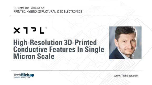
- High-Resolution 3D-Printed Conductive Features In Single Micron Scale
Speaker: Filip Granek | Company: XTPL | Date: 11-12 May 2021 | Full Presentation We introduce the ultra-precise deposition (UPD) technology for rapid prototyping of microelectronic devices. UPD allows maskless deposition of high-viscosity metallic and non-metallic inks with the printed feature size as small as 1 μm. XTPL technology answers some of the key challenges in the fabrication of high-density microelectronics, including the ability to print on complex 3D substrates and obtain structures with arbitrary shapes, including lines, dots, crosses, and meshes. Join TechBlick on an annual pass to join all live online conference or online version of onsite conference access library of on-demand talks (600 talks + PDFs) portfolio of expert led masterclass year-round platform https://www.techblick.com/ And do NOT miss our flagship event in Berlin on 17-18 OCT 2023 focused on Reshaping the Future of Electronics. This event attracts 550-600 participants from all the world and offers a superb ambience and dynamic exhibition floor. To learn more visit https://www.techblick.com/electronicsreshaped To see feedback about previous event see https://www.techblick.com/events-agenda
- Pulseforge | Use of Photonic Soldering to Enable High Quality Connections on T-Sensitive Substrates
This is auto-transcriped from the presentation without human control You are probably familiar with no Novacentric as as our kind of parent company and we have over the past of. Few months have migrated to to establish a new division within the company called Pulse Launch. So we bring the same innovative team to this foray, and we were working to solve a lot of the problems that that people are having with various processing challenges that they're facing. We're based in Austin, Texas. Then we always love to host you guys. So if you're ever in the Texas area of the United States, come visit us. So we're in the business of delivering light and we use that light to heat up or do some work on a different material. And the key that we bring to the table is that we can deliver this this energy in a very digital manner, in a non non-contact digital format, whereby we can really target what material we're heating up and we heat it up. Whereas the lead precisely and and repeated. So this heating can be done above the thermal equilibrium thermal damage threshold of most materials, enabling us to really get into creating value for our customers. This can be attributed. This type of pulsing can be attributed to processing a wide range of different materials. So that allows us to really get Spring Valley to a lot of different applications. So these are just some sample applications that we have. But for today's discussion, I want to talk about soldering and the ability for us to place components on substrates that have conductive pathways with few flashes of light actually solder. And the video you see on the left is a normalization of what that's happening. But on the right is actually a live video of how this happens within a two second timescale where the solder melt and the component moves it. We have a lot of advantages. One of the advantages that's very easily represented on the video is the ability to alter on a non flat surface, which is very unique because we don't actually have moving air. This also this ability also allows us to really process with low amounts of thermal input so we get a very good improvement and energy efficiency of the process as well as the tools are inherently smaller than the floor. And so we get a lot of space savings as well for our customers. Here's to to really be able to do solder components onto temperature sensitive substrates like PET, we need this delta. So this is a video of how the soldering is happening as measured by a thermal camera. And we can have a very, very high ramp rate of the of the component without really damaging the without really heating up the underlying substrate. So underlying so that this allows us to really process materials in a wide range of different substrates and different kind of conductive conductors. Enabling us to get. Performance comparable if not better than what we get in the reflow. So these are some chip components. These are showing the entire metallic chip components and how they behave. So these are line of sight exposure. We do work with components that don't have line of sight. So these are some examples of phones that don't have line of sight exposure and you're able to cure them. So we get really good attachment to it to a similar degree that we would achieve in a conventional reflow. But we can do this on temperature sensitive substrates like. So the tools that we have in the field that are able to deliver this performance are our kind of our small scale pilot line or our small production scale on the left, as you call the bag system. And underwriters are kind of in-line system that's more controlled for the process. There are a lot of advantages for this material. Of all the big advances in one minute, yes, we can take advantage of a lot of a lot of properties that are built into solder paste. So here's an example of these components being misplaced intentionally. And then using the sorting process, we can actually realign them and make it work. Another thing that we talk about, there's no inherent movement to the system, so we actually get better performance with smaller components. So we don't necessarily have the same limitations as heating up as you would have in a reflow process. With that, I would like to thank you for coming here and just give you an example of what we call the leaf design, which is a set of LEDs on top of a substrate that we get we give out a trade show. So if you run into any of my colleagues in near future trade shows, ask him for one. Thank you very much. Thank you very much for the excellent presentation. Very.
- Dupont MCM | Demonstration of high frequency 5G modules using LTCC | June 2022
This is an auto transcriped version of the talk without human control All right. Thank you very much. I appreciate the invitation to come talk about our materials. So first, I want to go into an introduction of motivation and 5G. So in response to society's increasing appetite for more and more data, telecommunication networks are looking to increase wireless communication, bandwidth and connectivity. And a critical aspect of this is the hardware, the devices that will that will need to operate at higher frequencies, at frequencies known as millimeter wave or about 20 gigahertz. Unfortunately, current device designs use materials that will not deliver the efficiency in terms of power utilization or with practical economics. But if you could integrate the semiconductor chips in the same modules as the passives and the switches and the filters and the antenna structures, this will shorten wiring distances and increase electrical efficiency as well as miniaturizing devices which are all good things using materials that I only use that only not only allow for increased integration, but also have stable performance at high frequency and at a myriad of operating conditions are critical to realize the advanced designs that these higher frequencies that will give us more data, but they also will provide hard hardware that will give a robust build out and avoid things like field failures or unnecessary maintenance cost in the field. And so that's why we focused on 5G. And so what I really am here to talk today about today is our product line called DuPont Green Tape Ltsc. And if you're not familiar with this technology, we take cast a ceramic slurry of precursor particles. It's a flexible tape that can be have vias punched in it filled with metal paste, have screenprint advanced screen printing of x, y, traces of conductors and then layers stacked, laminated and co fired at what's a relatively low temperature for ceramic processing and what results from that. I put on a chart here in the middle, a traditional printed circuit board that's ubiquitous around the electronics industry are ceramic. LTC is a similar 3D layer to construction of a circuit where here now instead of the dielectric being something like f floor, which is pre break filled epoxy or plated copper, we have a very high quality, dense ceramic material with metallization pastes created conductor lines. In this case, I'm going to talk about silver today. And so this is takes advantage of all the great material properties of ceramic but in the same laminar kind of construction to make very complex circuits. And like PKD, like PCB, you can make chip packages, components, all kinds of things. So LTC is a relatively mature technology. It's been around for four decades. It's been used for antennas and components and even antennas, but you can use it as a chip package. To date, it has somewhat fallen out of favor and has a current perception, and I would say a misperception that it's fundamentally hard for prototype or expensive or a costly process. The PCB is ubiquitous, LTSC is a little bit lower installed base, and so I think that's just a transient state of the technology. But really what justifies the use in revisiting this material is the great material properties. So I show here one of our systems, the lost tangent on the left here is the lowest for any commercially available material in the millimeter wave frequency regime. And you can see over a wide range of frequencies the loss stays very low, the dielectric constant is stable. But not only is it a good dielectric material, it's stable under a host of conditions. So under a wide temperature regime, the loss and dielectric constant don't shift. It's impervious to moisture or hermetic. And so there's no fear like there is in FR for printed circuit board materials that humidity will address dielectric properties and change device design. And in addition, the thermal properties are superior to any organic solution. So in order of magnitude higher thermal conductivity that's matched to the semiconductor devices and a strong flexible strength. So ceramics are fragile, but these ceramics are tough and so they're strong, rigid substrates. And material properties are not the deciding factor in how to make an electronics device, and we recognize that. So we partnered with a research institute in Taiwan and made what I show here is a module. The basis is ltsc. And so this is a multilayer package with antennas on one side and the ability to assemble the chips and passes on the other side. I show a picture of it fully assembled and a schematic of what it looks like in cross section. This was put into an into a system that's represented by this block diagram where all the ltsc is the emitter. We can characterize all kinds of antenna properties of this phaser array beam steering beam formed system. But the real proof here is that we can build a system that transmits 4K video up to ten meters across a conference room. And this is a relatively simple design that was quickly prototyped and really had no hiccups in thermal design, which is unusual for a high power, high frequency device with multiple antennas. And so we think this kind of references on kind of proves the point that LTC is a superior material and easier to design. And so in conclusion, I think LTC has a lot of myths associated with it. But if you think of it from a total solution standpoint, these great material properties that we're quite proud of can be utilized in a design when you think about the total cost of the whole solution. And although there may be some differences in the value chain and the prices, I think if you think of the total solution, it justifies the Watts already occurring increase manufacturing base. And so we'd like to talk to whoever would be interested and work with them to try and make designs to sort of unlock the power of these materials in current designs. Thank you. Speaker 100:06:44Well done, Brian. Impressive work. I've seen thumbs up and applause coming up the whole time during the presentation. So people like to talk and that this went smoothly is really great.
- SOLAIRES raising USD $2.1 million for their solar energy revolution
Victoria, B.C. (February 2022): Solaires Entreprises Inc (Solaires), a Canadian cleantech startup based in Victoria BC, is raising USD 2.1 million in pre-seed funding at a pre-money valuation of USD 9 million. Investors and recognized angel groups in British Columbia, such as eFund, Cindicates, and Keiretsu forum members are participating in this round. “We have developed a solution that will enable innovative solar energy applications to revolutionize solar energy harvesting. We are currently in advanced discussions with key partners for this product as they are interested in Solaires’ vitally important work in accelerating our transition to a low-carbon economy”, said Chief Development Officer, Ernest Daddey. The proceeds from the pre-seed round will be directed towards purchasing materials and equipment to ramp up the production capabilities of the company and scale up their product sales of Solar Ink™. “We are very grateful for the continued support we receive from our partners, our communities, and our investors. Our progress in the pre-seed raise and product launch has demonstrated that we have an excellent team and proven technology. Now onwards, we will be ramping up production and delivery to start order fulfilment,” said CEO & Co-founder, Fabian de la Fuente. About Solaires Entreprises Inc.: Solaires Entreprises Inc. is a Canadian cleantech company located in Victoria, focused on developing the next generation of solar cells by replacing silicon with perovskite through an innovative and sustainable manufacturing process resulting in affordable solar photovoltaics with higher energy conversion efficiency and higher stability. Solaires’ business model includes the sale of their product, Solar Ink™, and the licensing of their perovskite solar cell technology manufacturing process to selected roll to roll coaters, solar cell manufacturers, and OEMs. Solaires focuses its team of scientists on developing new and innovative patents relevant to the photovoltaic industry. Contact: Dr. Sahar Sam +1 (888) 464-2532 sahar@solaires.net For more information about Solaires, visit www.solaires.net
- IDS | High Output Rate Aerosol Printing for High Conductivity Printed Electronics | June 2022
This is an auto transcriped version of the presentation without any human control. Speaker 200:00:04Yes, we can hear you. We can see you and your slides are perfect. So you have your 5 minutes now. Speaker 100:00:09Okay. Thank you very much. So today we're going to talk about high output, aerosol printing for high conductivity, printed electronic applications. The first thing we're going to talk about is sort of the sweet spot for aerosol printing, the traditional sweet spot. And then we'll talk a little bit about what we're doing to enhance the aerosol printing capability and expand it into other areas. So the slides here show the typical sweet spot for for aerosol printing is fine printing of fine lines. A lot of effort for aerosol printing has been focused, no pun intended, on printing of very fine features. So we can reliably print features down to 15 microns. And with our and a lot of our customers actually have printed features at ten microns or less. The image on the right shows gold printed conductors, they're 20 microns wide at 100 micron, and they have really good line edge quality. I can show you some better higher magnification images of the type of image quality you would expect for our aerosol printing. Another unique advantage that we have for the aerosol printing is that we have a large working distance between the nozzle and the substrate that we're printing on. This really makes aerosol printing unique or provides a unique advantage over a lot of the other digital printing technology used used in printing printed electronics. So the printing stand up distance can be anywhere from 2 to 5 millimeters typically. And customers even recently have demonstrated ten millimeter stand up distance with good with good print quality. And it's one of the misnomers that we have talked about focusing of the aerosol stream, but in fact, it's actually largely carbonated as opposed to focus. So the large stand of distance gives us the ability to print over features such as the one shown here on the left, on the right, the this is the 3D printed dome structure. And we printed a strain gauge on here for one of our projects. And we did this with 3D three axis motion control for motion control, sorry for all the pop ups. And then I'm going to step into what we're doing now to really enhance our output rate as we start to kind of move more towards production applications or being able to print larger features and how we're doing that. One application that we're looking at is replacing wire bonding with the formation of stud months with printed forms instead. This is particularly useful for people in the medical field where they're making medical devices or high performance electronic applications, where the volume of of a single design is small or the throughput is anyway high make, high mix, low volume applications and so on. The image on the ratio is one of the stud pumps that we printed recently, and this is still under development, but the features about 40 microns tall and 70 microns wide on the bottom. And we've developed a unique formulation that allows us to kind of print these features with minimal overspray and get really good definition. And none of these bumps would generally be printed on to the conductive or the circuit substrate, and then the integrated circuit would be flip flip chip bonded to using the bumps. Part of what we've done recently, we've actually looked at our ink formulations and we've been able to increase our output rate by a factor of about 17 times by modifying and working with the writings that are able to be pretty aerosolized with viscosity, but also be able to output our printing technology. And then we also are some of the things we're looking at are at the high flow rates is also some better focusing capabilities. The image on the right shows a line we recently printed using some some advances in our focusing capabilities. We were able to output these printed lines at five millimeters. Print speed is five millimeters per second, a single pass, and the line is about 15 microns tall and about 90 microns wide at the base. And we're able to demonstrate using this technique also to print features up to 200 microns. And this is a significant advancement and our output rate material for a volumetric material output rate, I think this was like 5 million, 5 million cubic microns per minute, I believe was the calculation. We're also continuing to make sure that the performance of the Printheads remain consistent. The data on the right shows the typical tests that we're using on our practice for qualification, and it shows that the average deal this shows for a 70. Micron private line. We have an average standard standard deviation of the printed line with about three 3% over the eight hour period. And the tolerance on that is about 5%. The lines in the upper ratio of the lines that were printed for this eight hour test, the unique design for a print head really avoids clogging. And what was typically known is satellites are largely eliminated with the printing technology. The images on the lower right show the printed types of printed line edge quality you expect with the nano aerosol printing technology. In contrast on the image on the right shows, aerosol printing on a different technology from a different company that was more traditional. It was original aerosol printing technology. So our technology, with the way we're focusing using multiple air than they. Speaker 200:05:53Have one minute just just an issue. Speaker 100:05:56All right. Thank you. Allows us to avoid overspray and provides consistent, reliable, long term printing performance. Because of the high output rate, we're able to print features like the one being shown on the video on the right. So we're able to print features that have substantial thickness at a high output rate. This is a coil that's being printed on an embedded medical device that's being used as a stimulator. And so the coils actually have 20 or 20 ohms. They take about 10 minutes to print and they're used for both power transfer and telemetry for the embedded device. So you basically can power remotely and read the signals back from a patient. So between the medical embedded device and the step bumping application, these are two applications that we're looking at for the higher output rate, the printing technology. Thank you very much. Speaker 200:06:48Thank you. Thank you for the presentation, David, and thank you for joining us. As always. It's really interesting to learn about the capabilities of aerosol printing and amazing how what kind of features we'll.