Search Results
1031 results found with an empty search
- Accelerating the development of new value added materials
Speaker: Aaike van Vugt | Company: VSParticle | Date: 11-12 May 2021 | Full Presentation Join TechBlick on an annual pass to join all live online conference or online version of onsite conference access library of on-demand talks (600 talks + PDFs) portfolio of expert led masterclass year-round platform https://www.techblick.com/ And do NOT miss our flagship event in Berlin on 17-18 OCT 2023 focused on Reshaping the Future of Electronics. This event attracts 550-600 participants from all the world and offers a superb ambience and dynamic exhibition floor. To learn more visit https://www.techblick.com/electronicsreshaped To see feedback about previous event see https://www.techblick.com/events-agenda
- 3D printed biodegradable battery with the potential to slash electronic waste
Researchers at the Swiss Federal Laboratories for Materials Science and Technology (EMPA) have used 3D printing to create a sustainable new class of supercapacitors. The fully-3D printed battery, composed of a flexible cellulose and glycerol substrate, patterned with conductive carbon and graphite-laden ink, is able to withstand thousands of charging cycles while maintaining its capacity. Thanks to its biodegradable base, the novel cell can also be composted once finished with, potentially making it an ideal tool for tackling the world’s electronic waste issues. According to the EMPA scientists, the recent boom in electronic wearables, packaging, and Internet of Things (IoT) applications, has seen the global number of these devices rise to 27 billion. However, given their short life cycle, and the fact they tend to be powered by non-renewable lithium-ion or alkaline cells, many such products will eventually be landfilled, worsening the global ‘e-waste’ problem. The researchers’ findings are detailed in their paper titled "Fully 3D Printed and Disposable Paper Supercapacitors". In an effort to develop more eco-friendly energy storage devices, scientists have therefore begun to experiment with electrical double-layer capacitors, or ‘EDLCs.’ These high-capacity, fast-charging supercapacitors can at least partially be manufactured from biodegradable materials, potentially making them an ideal replacement for normal batteries, which often require specialized disposal services. Although a significant amount of research has gone into EDLC R&D, their varying parts such as electrodes and current collectors can be difficult to produce via a single manufacturing process. What’s more, many prototype EDLCs are partially-3D printed at most, necessitating their time-consuming and expensive assembly or post-processing, which makes them unattractive as commercial ventures. To streamline EDLC production and create an eco-friendly battery of their own, the EMPA team turned to DIW 3D printing, which they used to manufacture two half cells before folding them together. In practice, this meant printing the unit’s substrate base first, then depositing its electrode and conductive graphite-infused electrolyte layers on top, in a process that after some tweaking, yielded a functional battery. “It sounds quite simple, but it wasn’t at all,” said Xavier Aeby of EMPA’s Cellulose & Wood Materials lab. “It took an extended series of tests until all the parameters were right until all the components flowed reliably from the printer and the capacitor worked.” He added, “As researchers, we don’t want to just fiddle about, we also want to understand what’s happening inside our materials.” Once their supercapacitor prototype was ready, the scientists sought to test its charge retention by charging it to 0.5 V, before measuring its open surface voltage. According to the researchers, their device still had 30% of its charge remaining after 150 hours, putting its performance “in line with that of state-of-the-art carbon-based supercapacitors.” Interestingly, the researchers found that the capacity of their supercapacitor also fluctuated for two weeks after fabrication then settled, while it later remained functional after eight months in storage, and when they had finished their experiments and attempted to compost it, they were able to dissolve around 50% of its mass over the course of nine weeks. During testing, the team’s device was ultimately capable of powering a 3V alarm clock under mechanical stress, as well as operating at wildly varying temperatures. As a result, with further R&D, they say it could be deployed on a wider scale, to sustainably power low-voltage smart devices such as those used within environmental monitoring, e-textiles, or healthcare applications. For more information: https://3dprintingindustry.com/news/scientists-3d-print-biodegradable-battery-with-the-potential-to-slash-electronic-waste-198196/
- Smart bandage shows promise for chronic wound monitoring
A research team led by Professor Lim Chwee Teck from the National University of Singapore’s (NUS) Department of Biomedical Engineering and Institute for Health Innovation & Technology (iHealthtech), in collaboration with clinical partners from Singapore General Hospital, has developed a smart wearable sensor that can conduct a real-time, point-of-care assessment of chronic wounds wirelessly via an app. A world’s first, the novel sensor technology can detect temperature, pH, bacteria type, and inflammatory factors specific to chronic wounds within 15 minutes, hence enabling fast and accurate wound assessment. The research was published in the journal Science Advances "A flexible multiplexed immunosensor for point-of-care in situ wound monitoring". With a rapidly aging population, healthcare providers are seeing more patients suffering from non-healing wounds such as diabetic foot and chronic venous leg ulcers. It has been estimated that about two percent of the world’s population suffers from chronic wounds. The healing processes for these chronic wounds are often interrupted due to reasons such as infection and repeated trauma, leading to severe stress, pain, and discomfort to afflicted patients. For patients with diabetic foot ulcers, this can lead to more severe outcomes such as foot amputation. Timely care and proper treatment of chronic wounds are needed to speed up wound recovery. However, this requires multiple clinical visits for lengthy wound assessment and treatment, which adds to the healthcare cost. The NUS team’s innovation can help mitigate these consequences and relieve patients with chronic wounds from unnecessary distress. Current clinical assessments of wounds rely on visual inspection, or collecting and sending wound fluid to a centralized lab to detect and analysanalyzee specific biomarkers. The whole process usually takes about one to two days and may impede proper, timely, and precise medical interventions. Although there are recent developments in flexible sensors designed for wound care, they can only probe a limited set of markers such as acidity, temperature, oxygen, uric acid, and impedance to diagnose wound inflammation. In response to these current limitations, the researchers developed VeCare, a point-of-care wound assessment platform consisting of an innovative wound-sensing bandage, an electronic chip, and a mobile app. The bandage comprises a wound contact layer, a breathable outer barrier, a microfluidic wound fluid collector, and a flexible immunosensor. VeCare is the first wound assessment platform that can detect bacteria type and probe inflammatory factors, in addition to measuring acidity and temperature, within a single 15-minute test. The immunosensing bandage enables rapid assessment of wound microenvironment, inflammation, and infection state by detecting multiple chronic wound-specific biomarkers from wound fluid using an electrochemical system. The microfluidic wound fluid collector attached to the sensor directs and boosts wound fluid delivery to the sensor by up to 180 percent. The design ensures reliable sensing performance regardless of the ulcer shape or size. In addition, a chip integrated with flexible electronics is connected to the sensor to transmit data wirelessly to an app for convenient, real-time wound assessment and analysis onsite. The chip component, powered with a rechargeable battery, can be reused for subsequent applications. For more information: https://healthcare-in-europe.com/en/news/smart-bandage-shows-promise-for-chronic-wound-monitoring.html
- Optical Simulation to Develop Curved OLED and LCD Displays
Curved and flexible displays have risen in popularity in recent years and will continue to do so with high demand coming from several sectors. This is most visible, of course, in smartphones and tablets, where there is a constant need for innovation in order to keep consumer interest. Further demand is also emerging at a rapid pace from the automotive and lighting sectors. Thus R&D into next-generation displays remains strong. All of these applications require dedicated features for the control of light-guiding and outcoupling due to the curved geometry. However, most microtextures for beam shaping are designed for flat devices, and their appropriateness for curved geometries needs to be evaluated. In this video tutorial, Dr. Urs Aeberhard demonstrates how to use the Optics module of Laoss to rapidly model a curved display backlight unit. Urs is using Fluxim’s 3D ray-tracing tool Laoss Optics to determine the impact of curved geometries on beam shaping. He is also demonstrating how to design suitable structures to control light outcoupling via microtextures in backlight units for LCD displays. More information: https://www.fluxim.com/news/22/10/curved-displays-mastering-light
- MicroLED tool that can optogenetically stimulate, control and observe neural activity in the brain
A research team in the Department of Electrical and Electronic Information Engineering at the Toyohashi University of Technology has developed a MicroLED neural probe for neuroscience. This MicroLED tool can optogenetically control and observe neural activity in the brain. The work "Development of a neural probe integrated with high-efficiency MicroLEDs for in vivo application" was published in the Japanese Journal of Applied Physics. An LED probe with 16 MicroLEDs was fabricated in one shank and it was reported to effectively activate neural activity in the depth direction in the cerebral cortex in vivo. This design allowed for the realization of complex neural activity manipulation; however, electrophysiological experiments require the use of neural recording electrodes to capture the manipulated neural activity. Because the LED probe and neural recording electrode probe are different, it is necessary to precisely control the position of each probe and insert both devices for observation. Thus, the development of an integrated MicroLED and neural recording electrode probe is essential. New optogenetic technology that enables the manipulation and recording of single neurons in the deep regions has been realized; however, there are a few reports of such integrated probes. Furthermore, among those that have been reported, they are not suitable for neuroscience research because the light output of MicroLEDs is as low as several μW because of their small size. Although an increase in the MicroLED size leads to an increase in light output, this size increase also lowers the spatial resolution and increases the amount of stimulation-induced heat, resulting in more heat damage. As such, it is necessary to optimize the trade-off between light output and device size; in addition, the installation of highly efficient LED devices that suppress Joule heat is required. In this study, a neural probe with six micro-light-emitting diodes (MicroLEDs) and 15 neural electrodes was fabricated for optogenetic application. Local field potentials, which provide information about the neural activity, were successfully recorded using the neural probe, indicating the effectiveness of the neural electrodes. The MicroLEDs on the probe exhibited highly consistent current-voltage characteristics and sufficient light output of 20 mW mm−2 at 1 mA to manipulate neural activity. The light distribution in brain tissue was simulated to estimate the optical stimulation area and a number of optically stimulated neurons. The increase in LED temperature, i.e. ΔT, was investigated because high temperatures can damage brain tissue. A curve illustrating the relationship between ΔT and the wall-plug efficiency was derived. The wall-plug efficiency was increased 1.8 times by installing an Ag mirror on the back of a MicroLED. These results suggest that the MicroLED neural probe would significantly contribute to the development of neuroscience research-purposed optogenetic technology. More information:https://medicalxpress.com/news/2021-01-microled-neural-probe-neuroscienc
- PulseForge Soldering-Using flash lamp technology for conventional solder alloy reflow
Speaker: Rudy Ghosh | Company: NovaCentrix | Date: 11-12 May 2021 | Full Presentation Bio As the Technical Program Lead at NovaCentrix, Rudy Ghosh helps translate technical innovations into customer ready products. He works closely with NovaCentrix’s customers, technology partners, and collaborators across the world to solve technical challenges and identify new avenues for the application of NovaCentrix’s industry leading technologies in PulseForge tools and Metalon inks for printed and flexible electronics. As a technical expert in the printed electronics industry, he is often an invited speaker for a variety of printed electronics conferences. Rudy also works with the global business team to define and engage in commercial opportunities related to the technical program and furthers those areas of opportunity through industry outreach and engagement. Before joining NovaCentrix, Rudy was a Post-Doc at the Microelectronics Research Center at the University of Texas at Austin, where he led the Center’s research into the synthesis of 2D materials. Rudy holds a PhD in Physics from the University of North Carolina at Chapel Hill and a MS in Physics from the Indian Institute of Technology, Bombay. Rudy has authored over 30 publications in a variety of technical journals. Join TechBlick on an annual pass to join all live online conference or online version of onsite conference access library of on-demand talks (600 talks + PDFs) portfolio of expert led masterclass year-round platform https://www.techblick.com/ And do NOT miss our flagship event in Berlin on 17-18 OCT 2023 focused on Reshaping the Future of Electronics. This event attracts 550-600 participants from all the world and offers a superb ambience and dynamic exhibition floor. To learn more visit https://www.techblick.com/electronicsreshaped To see feedback about previous event see https://www.techblick.com/events-agenda
- DuPont's new silver pastes for In-Mold Electronics
DuPont Microcircuit Materials introduced an advanced suite of silver-bearing thick film paste conductors to enable In-Mold Electronic devices. The new conductors ME102, ME604, and ME614 have key advancements to improve thermoformability, conductivity, and fine line performance. These offerings enable high productivity, improved mechanical and electrical properties allowing extended freedom in the electronic design of In-Mold Electronics devices. These devices include next-generation LiDAR systems for autonomous driving or touch steering wheels with transparent 3D-shaped surfaces for enhanced user experience. Key advancements of the new ME range include: ME102 as a highly conductive thick film conductive paste for antennae, heater, and RFID functions ME604 as a general-purpose thick film conductive paste with improved thermoformability and conductivity ME614 thick film conductive paste with added laser ablation property for very fine line applications “This innovative new offering demonstrates a range of superior technical properties to meet different customer requirements. We are excited to introduce the ME product range to the market globally and expect a positive impact in accelerating the wider adoption of the emerging In-Mold Electronics technology”, said Peter Weigand, global automotive segment manager, DuPont Microcircuit Materials. For more information, visit: https://www.dupont.com/news/dupont-microcircuit-materials-introduce-silver-pastes.html
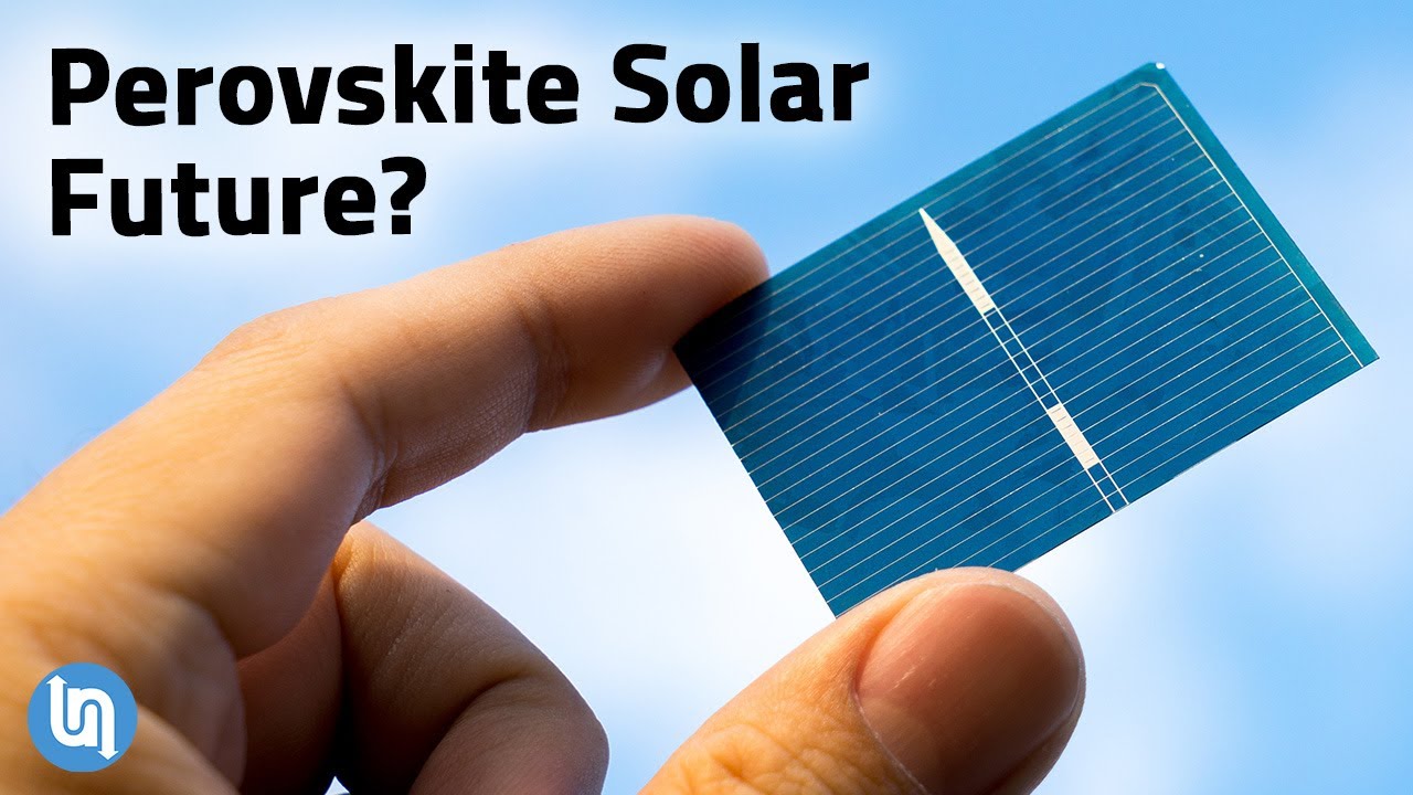
- The future high efficient, low carbon processed solar panel technology
What if we could build solar panels using materials that aren't supply-limited and with a lower carbon process? As well as achieving higher efficiencies at the same time? Perovskite solar panels have been promising that future for some time now, but where are they? And are they the future of solar panel technology?
- Combustion creates an inflatable braille display that changes its shape under the user's touch
Imagine an iPad or a Kindle for the blind, with inflatable braille that changes shape under a user’s touch. A Cornell-led collaboration has made a crucial component for such a technology: a haptic array of densely packed actuators that cause silicone membrane “dots” to pop up when triggered by combustion. The team’s paper, “Valveless Microliter Combustion for Densely Packed Arrays of Powerful Soft Actuators,” was published in Proceedings of the National Academy of Sciences. The lead author is doctoral student Ronald Heisser. One of the major hurdles for designing a dynamic braille display for electronics is figuring out how to apply the necessary amount of force for each dot. Previous attempts have usually involved motors, hydraulics, or tethered pumps, all of which are cumbersome, complex, and expensive, according to Rob Shepherd, associate professor of mechanical and aerospace engineering in the College of Engineering and the paper’s senior author. “Having something that can change its shape in a way you can feel, like real objects, doesn’t exist right now. There’s this tradeoff between having small actuators, and size and weight and cost. It’s so difficult,” Shepherd said. “Everybody’s been trying electromechanical systems. So we said, well, what if we don’t do that at all and we use combustion. Small volumes of gas can create powerful outputs.” The Cornell team collaborated with researchers from Technion-Israel Institute of Technology to design a system, composed primarily of molded silicone and microfluidic liquid metal traces, in which liquid metal electrodes cause a spark to ignite a microscale volume of premixed methane and oxygen. In their array design, this fuel flows through a series of independent channels, each leading to a 3-millimeter-wide actuator. The rapid combustion forces a thin silicone membrane at each site to inflate several millimeters. A magnetic latching system gives these dots their persistent form, and the whole system can be reset simply by pressing them down. Because there is no need for electromechanical valves, the actuators can be packed more densely together, resulting in a smaller, potentially portable system that still manages to produce large displacements at high force in under 1 millisecond. And since the fluidic elastomer actuators cool quickly, and so little fuel is required, a commercial version could be safely operated. The technology is also stretchable and conformable, and the researchers anticipate it could be incorporated into a range of applications, such as soft robots and wearable virtual reality equipment that simulates artificial touch. The biocompatible components could also be used for surgical tools that manipulate tissue or open blocked passageways in medical patients. The current system consists of nine fluidic elastomer actuators, but the researchers are hoping to scale that up and eventually create a full electronic tactile display. “For the past 30 years or more, people have been trying to pack actuators in an array really closely together,” Heisser said. “Touch, in a way, is more intimate to us than sight. The technology has real potential. I think our work shows there are more ways of thinking about this. Chemical actuation is really not something to be ignored.” For more information, visit: https://news.cornell.edu/stories/2021/10/combustion-creates-braille-display-electronics
- Toppan's Microfluidic Chips expected to be used for early cancer detection
LCD manufacturing technology was successfully applied to create prototype chips for specimen testing. Mass production can support the expanded use of microfluidic chips expected to be used for super-early cancer detection. Toppan, a global leader in communication, security, packaging, décor materials, and electronics solutions, has developed technology to manufacture glass microfluidic chips by photolithography.1 Mass production of microfluidic chips using the technology will make it possible to produce chips in larger volumes and at a lower cost than those manufactured via current injection molding technology, which involves injecting polydimethylsiloxane (PDMS), a type of silicone resin, into a metal mold. Photolithography is a fundamental technology honed by Toppan over 60 years in the electronics business and is used for the microfabrication of LCDs and master plates for semiconductor circuits. Microfluidic chips manufactured by this technology are expected to be used in the fields of in-vitro diagnostics and liquid biopsy (a largely non-invasive diagnostic technology requiring only a small amount of blood or other fluid samples), which is expected to see high levels of demand for applications including cancer diagnosis and clinical testing. Recent years have seen growing interest in liquid biopsy testing, which uses samples of blood or other fluids to enable super-early detection of cancer. Microfluidic chips manufactured by injection molding using PDMS are widely used for testing due to the material’s excellent biocompatibility and suitability for optical analysis. The low productivity for microfabrication when using PDMS and the high cost of liquid silicone as raw material, however, drive up the cost of chips, presenting an obstacle to more widespread use. To address this challenge, Toppan has developed technology for producing microfluidic chips by applying microfabrication technology based on photolithography techniques cultivated in the manufacture of LCD color filters. Specifically, channels (grooves or holes that allow liquid or gas to flow) with a width of 10 micrometers (micrometer=0.001 millimeter) to several millimeters and a depth of one to 50 micrometers are formed on a photoresist (light-sensitive material) coated onto a glass substrate. A cover with openings for injecting fluid samples or specimens is then applied over the cured photoresist. Microfluidic chips manufactured using this method have properties that are equivalent or superior to those of PDMS chips and can enable production in larger volumes and at a lower cost. “We have applied Toppan’s advanced microfabrication techniques to potentially enable mass production of something that can drive widespread use of medical testing techniques that reduce the burden on patients,” said Yuichiro Abe, manager of Development Planning in Toppan’s Electronics Division. “We will continue to work with our collaborative partners on pilot testing for commercialization of glass microfluidic chips and hope to establish photolithography-based mass production technology by March 2022.” For more information, visit: https://www.toppan.com/en/news/2021/10/newsrelease211007.html
- Advances in Polyester Film Substrates for Flexible Electronics
Speaker: Scott Gordon | Company: DuPont Teijin Films | Date: 11-12 May 2021 | Full Presentation Continued advances in Flexible Hybrid Electronics have required material suppliers to deliver improved functionality to the device developers in broad applications such as sensors, displays, barrier films, photovoltaics, medical diagnostics, consumer electronics, HMI (Human Machine Interface), and Flexible Printed Circuits (FPCs). Demands on the film substrate suppliers can vary widely, and polymer property requirements typically include: clean surfaces with low surface defects, optically clear films with low haze and iridescence, near zero thermal shrinkage for multilayer print registration and component attach via solder reflow, UV and Hydrolysis resistance, and VTM-0 Flame Retardance. Many requests also include an ability to further tailor the surface chemistry to improve and enhance the downstream processing performance. New commercial polyester film types have been introduced by DuPont Teijin Films, and their typical end use applications will be described. Fraunhofer FEP performs Roll-to-Roll film processing, and they are developing transparent and robust permeation Barrier Films for Flexible Electronics. The substrate choice is critical for optimized performance, and Fraunhofer FEP will describe their journey and key learnings. Join TechBlick on an annual pass to join all live online conference or online version of onsite conference access library of on-demand talks (600 talks + PDFs) portfolio of expert led masterclass year-round platform https://www.techblick.com/ And do NOT miss our flagship event in Berlin on 17-18 OCT 2023 focused on Reshaping the Future of Electronics. This event attracts 550-600 participants from all the world and offers a superb ambience and dynamic exhibition floor. To learn more visit https://www.techblick.com/electronicsreshaped To see feedback about previous event see https://www.techblick.com/events-agenda
- The formation of an IMC layer between the solder alloy & printed conductive copprint's paste
Additive Manufacturing of Electronics requires good soldering and is enabled with Copprint’s conductive copper inks, as demonstrated by the formation of an IMC layer (Inter Metallic Compound). This layer is formed during reflow between the solder alloy and printed conductive copper paste and is the index of good soldering. Full process details: Print copper traces on FR4 substrate with Copprint copper pastes. Soldering process – can be done even one week after sintering. Print off-the-shelf solder paste. (The most recommended paste is Henkel Loctite LF-318). Component placement. Standard reflow process. Die shear tests after the process indicated >3Kgf for 1206 SMD resistor soldered on Copprint’s LF360 with SAC305 Loctite LF-318. For more information, visit: https://www.copprint.com/news/#370