


11 August 2022
Molecular inks: UV sintering and extreme formability for complex IME applications
Molecular particle free inks can offer extreme formability and stretchability, allowing the design and production of 3D shaped and/or in-mold electronics parts with extreme curvatures and complex shapes. Arnold Kell and Julie Ferrigno showcased some unique properties of these inks- together with IME possibility- at a TechBlick conference in May 2022. Some unique features are:
1- UV sintering: you can see in the slide below how the transparent clear molecular inks can be UV sintered (x5 times faster than thermal cure). At first, the clear inks absorb very little UV light. However, as Ag particles begin to precipitate out, the absorption grows. The higher absorption in turn raises the temperature, accelerating the sintering and resulting in higher UV absorption. This process continues until the ink is fully sintered and then self stops because then the particles reflect the light back like a mirror.
2- Partial sintering compatible with InMold Electronics: as part of the IME process, a thermoforming step is required. In this step, the substrate temperature is raised in a controlled fashion to soften the material, allowing it to be formed. In the proposed scheme, the printed molecular inks are first only partially cured by UV light. The full sintering then takes place in-situ by the elevated temperature of the 3D thermoforming process. This is an interesting approach because it enables faster curing and also allows one to sinter molecular inks on low-T substrates like PC.
...

11 August 2022
R2R grown GaN LEDs on metal foils instead of expensive sapphire wafers?
R2R grown GaN LEDs and perhaps even GaN/AlGaN HEMT transistors on metal foils instead of expensive small-area sapphire substrates? This could be a breakthrough technology, bringing the robust and efficient inorganic LED technology to large-areas. In microLED displays, it could mean monolithic integration, leading to mobile-sized and large displays manufactured without a wafer-to-substrate transfer step. As shown below, iBeam Materials is developing such technology. It first planarizes a rough metal foil and then uses an ion beam to form a nm-thick layer with aligned grains. This 'template' then acts as the growth substrate in lieu of, say, a sapphire wafer. As seen below, this technology has already been used to demonstrate a functional GaN LED as well as a GaN/AlGaN HEMT. In July 2021 (when the results were presented at TechBlick) the PL was upto 70% of normal LEDs. However, a direct comparison is not yet fair as the standard approach benefits from decades and decades of accumulated know-how and production expertise. Currently, the LEDs are still not done in a R2R fashion, although the 'template' can be R2R manufactured on 20"-wide substrate. The next step of development will involve demonstrating a R2R MOCVD GaN growth. The R2R production of the template is not the bottleneck, but the growth of a thick (5um or so) GaN LED Finally, Vladimir Matias argues that this technology has the potential to lower cost of production by a factor x25. A detailed cost analysis is shown be...
8 August 2022
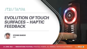
Evolution of touch surfaces - integrating decorative film, capacitive touch, and haptic function in
In the below presentation, Stefano Bianchi from SERISTAMPA SRL, shows a fully functional molded device made out of a combination of decorative film (in-mold decoration or IMD), printed capacitive touch film, and a haptic device. This injection molded device integrates push button, rotary knob, two linear slides, tactile feedback, etc
It is an excellent and complex demonstrator, truely the advancing the art of in-mold electronics to integrate aesthetics, sensing, and tactile feedback
Note that Seristampa is a leading industrial screen printing company specialized in advanced interactive service based in north of Italy. To reach this level of technological capability, Seristampa has evolved from aesthetical overlays/decorative parts to capacitive overlays/IML/IMD to capacitive films/printed electronics/IME and finally now to haptic device combining also all previous functionalities To learn more please visit Seristampa pages on TechBlick https://www.techblick.com/exhibitors Anne Rita Belke Gisella Tanzini
#printedelectronics #haptics #tactilefeedback #IME #InMoldElectronics #3DElectronics...
8 August 2022
3D-shaped mechanically-compliant soft force, pressure, or proximity sensors?
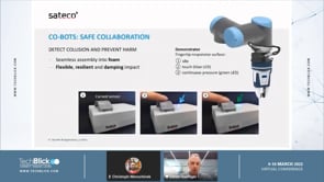
3D-shaped mechanically-compliant soft force, pressure, or proximity sensors with ease of integration and good reliability data? Daniel Haefliger from Sateco Group presents its non-printed technology based on multilayers of moulded conductive silicone. This is a unique technology. The sensor typically has a size of 10-40mm with a thickness of >3mm. It can measure forces in the range of 10-100 N with a resolution of around 0.1 N. The sensor can follow the direction of applied force for some 1mm. Interestingly, the exact behaviour of the sensor can be designed and adjusted by controlling the spaces between the layers to suit specific application requirements.
The technology is reliable. It is shown that at room temperature, it experiences only 5% driff when subjected to 5,000,000 cycles of 20N force. It experiences only 20% drift over full scale when subjected to 100k cycles of 20N force at much harsher conditions (T range: -40 - 85C | RH: 0-90%)
In clip from Daniel's full presentation given at TechBlick in March 2022, you learn about some unique applications of this technology, including:
1- Collaborative robots: these robots work alongside or in close proximity to humans. They are not caged as are typically industrial robots. As such, they require integrated soft 3D sensors to measure proximity as well as impact. This Sateco technology is uniquely suited to this application. 2- Smart steering wheel: the moulded silicone force sensor technology can be integrated within t...

11 August 2022
Phosphors or QD for color conversion in LCD and microLED? Which will win?
Phosphors or QDs for color conversion in LCD and microLED? Which will win? This is an interesting and evolving technology space to watch. James E. Murphy et al from GE Research have developed best-in class narrowband red and green phosphors, and are now evolving the technology towards microLEDs and on-chip integration
The red KSF phosphor is an excellent narrow band color converter for wide color gamut displays. It emits 5 peaks, each of which exhibits an ultra narrow 5-nm FWHM. The main peak is centred around 631nm. It is a stable material under high light flux and high temperature conditions. Indeed, it can be on-chip integrated as a direct replacement for existing yellow phosphors. It is a major commercial success with >19 licensees and >40 BILLION (and growing) KFS-containing LEDs sold worldwide into the display industry.
As the slide below, presented at TechBlick July 2021, shows, the KFS technology is evolving. At first in 2014, the average particle size was a 25-30um. It is now down to 3-9um and evolving towards sub-micron and even nano-sized particles, enabling direct integration with microLEDs of today and tomorrow! This is an important technology trend because it brings the QD vs phosphor competition even to the microLED space (previously QDs were the only game in town due to their small size)
Furthermore, GE's KSF can now be formulated into air-stable inks based on encapsulant-free phosphors suitable for inkjet printing without nozzle clogging. It means that...

9 August 2022
"The Future of Electronics RESHAPED" Event Reports High Demand For Exhibition Booths & Attendees
TechBlick, the leading platform for emerging technologies, has reported high demand for both exhibition booths and attendee places at its inaugural in-person event which takes place on 12 & 13 October at the High Tech Campus in Eindhoven.
The Future of Electronics RESHAPED conference and exhibition is the most important upcoming industry event in printed, hybrid, 3D, in-mold, textile & wearable electronics. As well as a world-class agenda and exhibition the event will also feature expert-led masterclasses and company tours to some of the innovative companies in the Eindhoven area.
Khasha Ghaffarzadeh, CEO of TechBlick reported "We were surprised at the high demand for exhibition booths and fortunately we were able to secure some additional exhibiting space. But we still have a waiting list of companies wishing to exhibit. We have seen the same high demand for attendee places with companies excited by the quality of the speaker programme and exhibitors. This event will be where the world’s printed electronics industry connects and does business and is an important new event in the emerging technologies calendar"
The world-class agenda features speakers such as Meta/Facebook, GE Healthcare, ASML, Airbus, Forvia, Schneider Electric, Stabilo, Forvia, Novo Nordisk, Identiv, JC Decaux, ABInBev and many more. See the full speaker list here. The vibrant exhibition floor features over 50 exhibitors including NanoDimension, DuPont, Eastman Kodak, FujiFilm, Henkel, Applied Mate...

8 August 2022
High-res metalization of 2D and 3D object made from glass, ceramic, PET or thermosets?
The traditional LDS (laser direct structuring) process is fantastic but only works on special plastic substrates containing an sub-surface activation particles. This limits the choice and functionality of materials. Firstly, it typically does not work with glass, ceramics, PET or thermosets. Furthermore, the addition of activation particles can render a transparent material opaque or eliminate bio-compatibility. Furthermore, the linewidth resolution is typically around 80-100um (but can be pushed further down) with surface roughness of 20-30um
Nouhad Bachnak , 3D-MID from Sunway Communication unveils a new process below, which promises to overcome these limitations. Here, the process first involves a special laser structuring process followed by a so-called chemical activation step. After this step, the structured and activated part undergoes typical plating (Cu-NiP-Au)
The details of the chemical activation step - possibly the most important step- were not disclosed. Nonetheless, the disclosed examples and results indeed suggest that it can work on glass, ceramics, thermosets, etc.
This is an important development and advancement of the technology, because it greatly lessens the limits on the choice of materials which can be 3D metallized with bulk-like properties and solderable surfaces
Furthermore, it is argued that this process- presumably when optimized- will achieve 5um linewidths with a surface roughness of just 2-3um (great for antennas, for example). It can also ...
8 August 2022
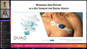
Smart skin patches: a key enable of digital technology
Smart skin patches are a rising trend, finding applications in sleep monitoring, EEG and brain activity monitoring, cardiovascular monitoring, and even in electrical stimulation of neurons, muscles, and other areas. These patches must meet many criteria- from signal quality to bio/skin compatibility to wearable to breathability to stretchability and to low cost production. Here, you will hear from Pauline Hibon on the requirements for skin patches as well as a general overview of some potential health-related applications To achieve low-cost volume production, screen printed electronics is essential. Quad Industries is well positioned in this area with its 1M/year patch production capacity. It can do R2R and S2S screen printing in Belgium and Slovakia, respectively. More importantly, it has already built extensive know-how and production expertise in the field with different designs and is thus an excellent prototyping and production partner. To learn more and visit the Quad Industry team, join the global industry in Eindhoven (the Netherlands) on 12-13 OCT 2022 https://www.techblick.com/electronicsreshaped Arne Casteleyn #printedelectronics#skinpatches#wearablesensors#medicalwearablesensors#eeg#BCI#insomnia#heartrate...