18 August 2025
VTT | Bringing Medical Technology from Innovation to Patient Care
#PrintedElectronics #MedicalTechnology #FlexibleElectronics Author: Antti KEMPPAINEN | Email: antti.kemppainen@vtt.fi
Bringing medical technology from innovation to patient care is slow and costly due to the complexity of the needed technologies and regulations. VTT’s pilot environment for medical devices, based on printed and flexible electronics and photonics technologies, accelerates the market entry of patient-friendly innovations. We are Exhibiting in Berlin. Visit our booth at the TechBlick event on 22-23 October 2025 in Berlin . Contact us for your special discount coupon to attend The medical device pilot enables the production of small and middle-size prototype series for pre-clinical studies using advanced flexible electronics, photonics, microelectronic, and microfluidic components and integration manufacturing technologies. These technologies facilitate the development of comfortable-to-wear, skin-like wearable sensors combined with wireless communication and data processing functionalities. Key application areas for the pilot line include preventive monitoring of cardiovascular diseases, metabolic syndromes, early cancer detection and recurrence, as well as rapid diagnostics. Our Key Infrastructure:
State-of-the-art ISO7 cleanroom Flatbed automatic screen printer with 500 mm x 500mm and Flatbed Computer-to-Screen (CtS) screen exposure system, UV and IR belt oven Automatic component assembly line for large area flexible PCBs High-capacity 3D X-ray Microscopy,...
13 August 2025
MicroLED and AR/VR Connect 2025: The Year’s Must-Attend MicroLED and AR/VR Display Industry Gathering
Introducing the program for MicroLED Connect 2025 and AR/VR Connect 202 5 (Conference and Exhibition, 24 &25 Sept 2025, High Tech Campus, Eindhoven, Netherlands)
This event is shaping up to be the definitive global forum for microLED and AR/VR display professionals, offering an exceptional program, vibrant exhibition, and unmatched networking opportunities. In this preview, we’ll spotlight several speakers, showcase selected conference themes, and give you a glimpse of what awaits in Berlin. For the complete agenda and event details, click here.
Mass Transfer – From Wafer to Display In many icroLED manufacturing platforms, at least one major transfer process is required—often two. Typically, devices move from the epiwafer to an intermediate interposer substrate and later from the interposer to the final display. Executing this step with precision, speed, and cost efficiency remains one of the industry’s most persistent challenges. At MicroLED Connect 2025 , leading innovators will unveil new solutions:
Coherent will present a fully integrated laser-based mass transfer system designed to handle donor wafers and receiver panels—whether they’re backplanes or temporary carriers. Offering exceptional throughput, yield, and flexibility, the system can manage even the tiniest microLED dies.
Holst Centre will introduce a proprietary release stack enabling rapid, selective microcomponent release with adaptive pitch using a cost-effective laser source. Recent results sh...
12 August 2025
Global Map of The Future of Electronics RESHAPED conference and exhibition
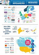
The Future of Electronics RESHAPED ECC, Berlin, Germany | 22 & 23 OCT 2025 Join us in Berlin on 22–23 October 2025 for The Future of Electronics RESHAPED — the global home of Additive, Printed, Sustainable, Hybrid, Wearable and 3D Electronics. World-Class Agenda - 100 Onsite Talks From Around the World! The map below highlights where our speakers for The Future of Electronics RESHAPED event are coming from — a testament to the truly global scope of our agenda. World-class experts will showcase the latest innovations and application developments. Register NOW at early bird rate Perovskite Connect This year, we are excited to co-locate the first-ever Perovskite Connect event alongside The Future of Electronics RESHAPED conference and exhibition. There will be a combined agenda. Perovskite Connect is the only event worldwide dedicated to the fast-growing perovskite industry. The speaker map below shows just how global this event also is — with world-leading experts and innovators joining us from across the globe. All attendees will have full access to both events Global Exhibition Floor - over 90 exhibitors from around the world An incredible tabletop exhibition featuring 90+ companies . Here you can immerse yourself in the world of Additive, Printed, Sustainable, 3D and Wearable Electronics! Explore NOW ACT NOW: Exhibition Booths Almost Sold Out The exhibition floor is almost sold out with only a few spots available. Contact Tom@TechBlick.com now if you wish to join...
8 August 2025
TechBlick Insights: Shear thinning, printed MCUs on PET, Ultrafine metal mesh films, perovskite solar vs Si solar, perovskite stability, microdispensed QDs for microLEDs, and more
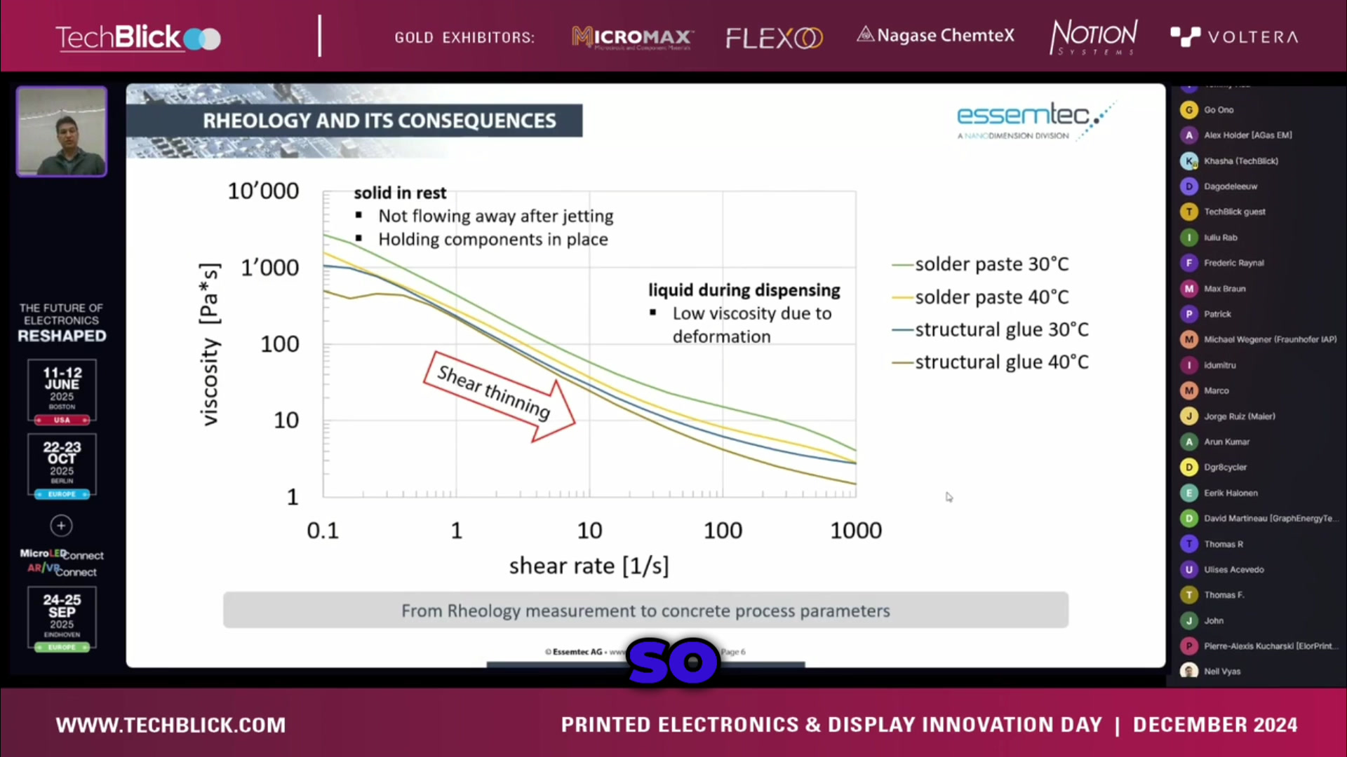
In this newsletter we cover the following Shear thinning of jetted solder and glue for assembly Fully printed double sided MCU on PET substrates? Ultrafine Cu mesh for transparent conductive films for touch, heating, security, etc film applications? Perovskite solar panels outperform the current silicon-based commercial panels, but what about cost? Perovskite solar panels are highly promising not just for utility-grade, but also for indoor light harvesting. Perovskite encapsulation for enhanced stability Microdispensing quantum dots for color conversion How will perovskite panels perform in the 'real world'? We cover these points by sharing short (1min or so) handpicked snippets from their live recent talks at TechBlick, Future of Electronics RESHAPED and Perovskite Connect conferences and exhibitions Join us at TechBlick’s Future of Electronics RESHAPED conference and exhibitions in Berlin on 22 and 23 OCT 2025. This is the global home of the additive, printed, 3D hybrid and sustainable electronics, bringing the entire value chain together, from innovators to suppliers and end users. This year as a special theme we will also collocate Perovskite Connect alongside the same show Explore program here now: The Future of Electronics RESHAPED Shear thinning of jetted solder and glue for assembly Shear thinning is one of the most important physical phenomena in jetting - or in fact in all of printed electronics! This is the physical mechanism on which much of the printed e...
15 August 2025
HPCaP: A New Technology for MicroLED Manufacturing
Authors: Julien Vitiello, Elisa Duquet, Louis Caillard, Achille Guitton, Marc Pascual, Maroua Ben Haddada, Frederic Raynal, Amin M’barki Corresponding author: julien.vitiello@hummink.com Hummink S.A.S, 5 rue Charlot, 75003 Paris, France Keywords: Display repair, additive manufacturing, High Precision Capillary Printing (HPCaP), capillary forces, Atomic Force Microscopy (AFM) Abstract In the field of display repair, particularly for OLED and microLED technologies, there is a growing need for precise and scalable solutions to restore high-resolution defects without compromising performance. While several repair methods exist, they often fall short in resolution, versatility, or ease of integration. High Precision Capillary Printing (HPCaP) overcomes these limitations by leveraging capillary forces and mechanical resonance to deposit inks with micron and sub-micron precision, enabling accurate, reliable, and non-destructive repair of critical display components. 1. Introduction According to MarketsandMarkets the global display market size is expected to reach around USD 174 billion in 2029 growing at a CAGR of 5.1% from 2024 to 2029. The increased demand for displays in various industries especially the IT and healthcare industries, and the increased demand of interactive displays such as wearable devices, AR/VR products in addition to the adoption of flexible displays are the major factors driving this market growth. We are Exhibiting! Visit our booth at the MicroLED Connect...
12 August 2025
Perovskite Connect 2025: The Global Stage for Perovskite Solar Innovation
Perovskite Connect 2025 is shaping up to be the must-attend event for the perovskite industry , bringing together leading innovators, researchers, and manufacturers from across the globe.
Taking place on 22–23 October 2025 at the ECC in Berlin , this specialist conference will run alongside the flagship Future of Electronics RESHAPED show.
The agenda will spotlight the entire perovskite value chain — from materials and production processes to cutting-edge applications in solar energy and beyond.
In addition to its high-level talks, Perovskite Connect will offer an international exhibition and abundant networking opportunities.
In this preview, we highlight just a few of the speakers and themes that will define the event. You can view the full program and details here .
Next-Generation Perovskite Solar Developers In an earlier feature , we introduced several perovskite PV pioneers — including Microquanta, Oxford PV, Perovskia, and Swift Solar. Perovskite Connect 2025 will welcome many more notable solar technology companies:
Halocell Energy will unveil its fully scalable roll-to-roll printing process for producing lightweight, flexible perovskite solar modules. These modules are optimised for low-light conditions and extended lifetimes, making them ideal for IoT devices requiring long-term autonomous operation. Beyond Silicon (USA) will focus on its solution-processing method for manufacturing bifacial perovskite/silicon tandem panels, offering potential c...
11 August 2025
Heraeus Electronics | Thick Film Whitepaper: Large-Format Printing of PTC 4980 Self-Regulating Heater Inks
Zachary Kelly, PhD . - Senior Research Scientist, Heraeus Electronics, Conshohocken, Pennsylvania Introduction Understanding PTC 4980 and Its Benefits Key Features of PTC 4980 Design Principles for PTC Heating Solutions Case Study: Improving Large-Format PTC Heater Performance 5.1 Initial Challenges Identified 5.2 Optimized Design and Manufacturing Process 5.3 Key Takeaways and Industry Implications Conclusion We are Exhibiting in Berlin. Visit our booth at the TechBlick event on 22-23 October 2025 in Berlin . Contact us for your special discount coupon to attend This paper has been carefully compiled by Heraeus Electronics. Although the content is considered accurate, we cannot guarantee that this paper is suitable for any application. The descriptions and engineering data shown here have been compiled by Heraeus Electronics using commonly accepted procedures, in conjunction with modern testing equipment, and have been compiled as according to the latest factual knowledge in our possession. 1. Introduction Printed electronics have revolutionized heating solutions across industries by enabling cost-effective, scalable, and customizable manufacturing processes. One of the critical advancements in this field is the use of Positive Temperature Coefficient (PTC) resistor pastes for self-regulating heaters. These materials offer inherent temperature control, reducing the need for external regulation mechanisms and ensuring safer, more energy-efficient heating solutions. Heraeus El...
7 August 2025
VueReal | Unlocking MicroLED’s Potential: Why Reference Design Kits Are the Key to Mass Adoption
Brad Martin , VueReal | bmartin@vuereal.com MicroLEDs promise to reshape the future of displays and lighting - with higher brightness, lower power consumption, and longer lifespans than OLEDs. But for most innovators, that promise has remained just out of reach. Not due to lack of ideas or demand, but because of one persistent barrier: access. That’s now starting to change, thanks to the arrival of Reference Design Kits (RDKs): pre-integrated microLED modules that empower engineers, designers, and developers to prototype and experiment - without custom fabrication, high-volume commitments, or massive investment. By dramatically lowering the barrier to entry and leveraging flexible manufacturing methods, RDKs are unlocking a new era of innovation - accelerating both the pace of discovery and the path to mass adoption. We are Exhibiting! Visit our booth at the MicroLED Connect & AR/VR Connect in Eindhoven on 24-25 September 2025 The Real Bottleneck: Access, Not Imagination Unlike OLED panels - which are widely available for prototyping and development - microLEDs have historically been locked behind technical and supply chain hurdles. Most companies simply can’t get their hands on the technology. Traditional microLED manufacturing typically requires highly specialized equipment, high-volume commitments, and extensive engineering integration, putting it out of reach for the majority of companies. Even those who want to explore microLEDs in earnest are left to imagine ...


