top of page
Perovskite-Connect white-Small.png
21-22 October 2026  |  Berlin, Germany

Co-located with the Future of Electronics RESHAPED

Masterclasses & Tours

On-Site Masterclasses (TBC)
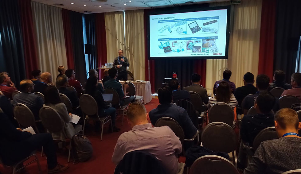
There will be multiple parallel tracks of industry-led masterclasses on 20 October 2026, the day before the conference and exhibition, as part of the co-located show. Each 45-min masterclass will cover a technology or application in detail, offering an insightful blend of practical, technological and application knowledge. 

These masterclasses will be delivered by industry experts & may involve live demonstrations. To give you a sense of the classes, please see our past programs here: Berlin 2025Boston 2025, Berlin 2024, Boston 2024, Berlin 2023Eindhoven 2022.

See the topics of the classes you can expect in 2026.


All atendees will be able to move between tracks at the end of each class. The numbers in each class are limited to 50, and will be allocated on a first come, first served basis. All masterclass presentations will be recorded and available along with the PDF slides for all attendees on-demand one week after the event.

Track 1
Track 2

See all accessible masterclasses in the full joint masterclass program with the Future of Electronics RESHAPED event. 

Attendees have access

to the full program

Masterclasses | Track 3
Masterclasses | Track 1
Celanese

9:00 AM

Polymer Thick Film Master Class

Saeed Madadi

Celanese

Saeed Madadi

This class introduces a detailed view on polymer thick film paste conductor technology. It comprises a descriptions of its main constituents, their respective functions and its critical parameters. An insight into resin and metal powder technology is given and the range of substrate materials and their properties discussed. Paste manufacturing steps and functional testing schemes for quality
assurance are summarized. Beyond screen printing alternative off- and on-contact deposition technologies as well as downstream processes are reviewed. The class closes with an overview of typical industrial applications.

University of Coimbra

10:00 AM

From Liquid Metal droplets to stretchable, self-healing, and sinter-free printed hybrid electronics

Mahmoud Tavakoli

University of Coimbra

Mahmoud Tavakoli

When it comes to stretchable electronics, e-textile, smart gloves, and wearable patches, Liquid Metals (LMs) are becoming the number one choice for most researchers. But research on LMs are also entering fields of energy storage, thermal interfaces, displays, energy harvesting, and even carbon capture. This is due to the excellent combination of electrical and thermal conductivity and fluidic deformability, that makes liquid metals the first choice for many applications. However, unlike the electrically conductive inks and pastes, LMs are not easy to deposit and pattern, they are smearing, and interfacing them with microchips is not straight forward. The good news is that these problems are being addresses rapidly, and there are already some steps toward commercialization of LM based electronics.

In this master class I will summarize the research on liquid metals during the last 15 years, and will demonstrate various aspects of liquid metals. The talk will be divided into 3 sections: Materials (Liquid Metals, LM composites, LM micro and Nano droplets), Fabrication Techniques (Deposition, Patterning and Microchip Interfacing) and Applications. I will talk about the results of electromechanical testing, and durability of circuits when subjects to over 100, 000 strain cycles. I will as well talk about the applications in the space of smart textiles, wearable patches, additive manufacturing, and mechanical sensing, and how some of the top manufacturers (e.g. in automotive sector) are already adopting solutions. If time permits, I will briefly talk about how LMs are entering the energy storage field, both as current collectors, and as active electrodes.

RISE

11:00 AM

The Role of Bio-based Materials and Additive Manufacturing in Achieving Sustainability Goals for Electronics

Jesper Edberg

RISE

Jesper Edberg

Electronic waste (e-waste) poses a pressing global challenge with the World Health Organization (WHO) reporting a staggering annual generation that exceeds 50 million tonnes. Less than 20% of this waste is recycled, highlighting severe environmental and health risks associated with the disposal of hazardous materials such as lead, mercury, and flame retardants. This challenge is further compounded by the overreliance of the global economy on rare earth elements and critical raw materials. Addressing this crisis requires a concerted effort to align with the United Nations Sustainable Development Goals (SDGs), particularly Goal 12 (Responsible Consumption and Production), which emphasizes reducing waste generation and promoting sustainable practices. Achieving this goal requires a paradigm shift in the electronics industry. Our course delves into the urgent need for sustainable materials and manufacturing methods within electronics. We explore alternatives to synthetic, often non-sustainable materials like PFAS (per- and polyfluoroalkyl substances) which persist in the environment and harm ecosystems. - Enter biobased materials—nature-inspired alternatives: Derived from renewable sources like trees, plants and algae, these materials offer a greener path. We’ll explore their properties, applications, and potential to revolutionize electronic design. - Additive Manufacturing and Printed Electronics: Create intricate electronic components layer by layer, minimizing waste and energy consumption for thin flexible solar panels, printed circuit boards, sensors, displays and more. We explore how these innovative techniques can reduce environmental impact. Join us on this journey toward sustainable electronics. Let’s design a future where innovation meets responsibility.

Beckermus Technologies

12:00 PM

Chip Interconnections for Flexible Printed Electronics.

Aviv Ronen

Beckermus Technologies

Aviv Ronen

In this masterclass we will learn the packaging hierarchy and learn how the chip interfaces and structure can help us in building a reliable electronic system. We will see how wire bonding, although famous, is not suitable for the flexible electronic eco-systems and than we see how flip chip bonding is better but still has it disadvantages.
We will see how solders and conductive adhesive has their pros and cons and how they both suffer from thermal mechanic stresses when bonding in elevated temperatures. Therefore, we will see why there is a motivation for lowering this temperature not only because the materials cannot withstand these elevated temperatures.

Masterclasses | Track 2
Arkema and KEMET

9:00 AM

Electroactive Polymers & Applications Focus on sensors & Actuators

Fabrice Domingues Dos Santos | Valerio Zerillo

Arkema and KEMET

Fabrice Domingues Dos Santos | Valerio Zerillo

In this Masterclass we will introduce the use of electroactive polymers for organic, printed and flexible electronics.Electroactive polymer is a class of different materials that convert electrical energy in Mechanical energy.Different types of electroactive polymers exists : Dielectrics, ionic, ferroelectric, Relaxor ferroelectric. Among them, ferroelectric polymers do the other way, converting mechanical energy into electrical energy. With these unique properties EAP find numerous applications and developments in printed and flexible actuators, sensors, energy-harvesters etc..In this Masterclass, we will introduce the different class of electroactive polymers and their applications.We will then focus on the processing and emerging applications of ferroelectric Polymers in sensors.In a third par we will introduce the use of electroactive polymers in flexible applications from AR/VR to Medicals.

TracXon, Lohmann

10:00 AM

R2R Flexible Hybrid Electronics: printing, assembly and testing

Ashok Sridhar | Volker Lutz

TracXon, Lohmann

Ashok Sridhar | Volker Lutz

In this joint masterclass by TracXon and Lohmann, an in-depth view of R2R manufacturing technologies that are essential for next-gen Wearables and IoT devices will be provided, based on practical examples.
These technologies include, but not limited to, R2R screen printing, SMD component assembly, downstream conversion processes such as lamination and die cutting. Furthermore, key considerations on materials selection will be highlighted.
Different testing methods and protocols that are essential in qualifying the IoT and Wearable devices will also be introduced in this masterclass. Based on experience we will provide an estimation of manufacturing scales to adopt increasing demand for new products.

Printed Electronics Ltd

11:00 AM

Digital Additive Manufacturing of Electronics: Inkjet, Aerosol, EHD Printing, Microdispensing and Beyond

Neil Chilton

Printed Electronics Ltd

Neil Chilton

In this masterclass, you will learn about all key digital additive techniques for manufacturing electronic devices - in 2D, 2.5D, and 3D. These techniques include inkjet printing, aerosol printing, electrohydrodynamic printing, microdispensing, and beyond. This class introduces the techniques and include practical insights and real-life application orientated advice on technology use, selection and operation

ImageXpert

12:00 PM

Techniques for optimizing an inkjet printing process for printed electronics

Jochen Christiaens

ImageXpert

Jochen Christiaens

In this masterclass, ImageXpert will discuss new technologies for the development of printed electronics. These tools allow you to build a better understanding of your inkjet process, improve performance, and accelerate your rate of development. We will explore the latest analysis tools, from new dropwatching technologies to smarter inspection tools."

Masterclasses | Track 3
Tours-collage.jpg
page-bg_edited.png
Company Tours (TBC)

Click below to explore tours in past events

The tours are open to attendees of the morning masterclasses


Places on the tours will be allocated on a 'first come, first served' basis. 

The tours will leave at 1.30pm and attendees should meet at the registration desk.  Transportation will be provided and the tours are expected to return to the Estrel by 6.00pm.


Confirmed tours include Fraunhofer IZM, Fraunhofer IAP, Helmholz Zenrum Berlin, Adlershof Research Park, and others

CONTACT US

KGH Concepts GmbH

Mergenthalerallee 73-75, 65760, Eschborn

+49 17661704139

chris@techblick.com

TechBlick is owned and operated by KGH Concepts GmbH

Registration number HRB 121362

VAT number: DE 337022439

  • LinkedIn
  • YouTube

Sign up for our newsletter to receive updates on our latest speakers and events AND to receive analyst-written summaries of the key talks and happenings in our events.

Thanks for submitting!

© 2025 by KGH Concepts GmbH

bottom of page