


9 September 2025
Choosing the Right Inkjet Printhead for Printed Electronics
Author: Kyle Pucci, kyle@imagexpert.com , ImageXpert The ImageXpert Perspective Inkjet printing has been around for decades, but in the world of printed electronics it is still an emerging technology — one that is opening doors to applications that traditional coating and deposition methods cannot reach. At ImageXpert, we have had a front row seat to this evolution. For more than 30 years, we’ve helped engineers and researchers understand, test, and optimize inkjet systems. Our equipment is found in hundreds of labs worldwide, giving us the chance to see firsthand what works, what doesn’t, and what separates a laboratory experiment from a production-ready process. Unlike print shops or graphic arts applications where speed and cost are the primary drivers, printed electronics demand precision and adaptability. The fluids are often unconventional: nanoparticle dispersions, high-viscosity coatings, or conductive inks. The layers can be extremely thin, sometimes just a few hundred nanometers, or conversely quite thick, exceeding one hundred microns. In every case, the choice of printhead determines whether the process succeeds or fails. We are Exhibiting! Visit our booth at the MicroLED Connect & AR/VR Connect in Eindhoven on 24-25 September 2025 Over the years, we’ve worked with companies who are brand new to inkjet, guiding them through early ink trials, waveform optimization, and eventually into pilot production. We’ve also partnered with seasoned electronics manufacturers wh...

8 September 2025
Introducing the Program - Smart surfaces and sensors
Why Should You Join TechBlick's The Future of Electronics RESHAPED? The Future of Electronics RESHAPED conference and exhibition (22 & 23 OCT 2025, Berlin) is set to be the most important event of the year focused on additive, hybrid, 3D, sustainable, wearable, soft and textile electronics. This year the program features a world-class agenda with over 100 superb invited talks from around the world, 12 industry- or expert-led masterclasses, 4 tours, and over 90 onsite exhibitors. In this article, we discuss and highlight various innovative talks at the event around the theme of smart surfaces and sensors. In future articles, we will cover further technologies including smart surfaces, sustainable electronics, printed medical electronics, novel materials and beyond. Explore the full agenda now and join the global industry in Berlin on 22 & 23 OCT 2025. Let us RESHAPE the Future of Electronics together, making it Additive, Hybrid, 3D, R2R, Soft, Flexible, Wearable, Textile and Sustainable. 🚨Register before 12 September to save 200 Euros on top of early bird discounts. This is a one-time offer. The coupon can be obtained here🚨 Toyota – Michael Rowe presents technology opportunities beyond automotive , showcasing cross-industry applications of actuator, sensor, and material innovations. Highlights include shape memory alloy (SMA) wire actuators delivering lightweight, translational motion with integrated feedback; near-IR reflective pigments enabling hidden data transfer fo...

1 September 2025
MicroLED & AR/VR Display Innovations: Mass Transfer, Wafer Metrology, Red GaN, Perovskite QDs, Smart Glasses, and Scalable Manufacturing
We cover these points by sharing short (1min or so) handpicked snippets from their live recent talks at TechBlick and MicroLED Connect conferences and exhibitions In this newsletter we cover the following MicroLED Wafer Metrology and Calibration Strategies Assessing the Practicality of MicroLED Displays for Mass Production Stamp-Based Imprinting for AR Waveguide Manufacturing Advances in Mass Transfer Processes for MicroLED Chip Integration VR vs. AR: Market Outlook and Growth Limitations Perovskite Quantum Dots for High-Density Color Conversion Challenges and Advances in Native Red MicroLED Efficiency Etching and Deposition Solutions for MicroLED Materials Progress Toward Emissive Quantum Dot–EL Displays Cubic GaN as a Novel Platform for Scalable MicroLEDs Wafer-to-Wafer Integration for MicroLED Microdisplays MicroLED Smart Glasses and Market Update for AR Applications Integrated Production Platforms for Scalable MicroLED Manufacturing Join the MicroLED Connect + AR/VR Connect 2025 on 24 & 25 Sept 2025 at the High Tech Campus in Eindhoven (Netherlands). Explore full agenda here and register before 12 Sept when the FINAL early bird rates expire https://www.microledconnect.com/ https://www.microledconnect.com Manufacturing Processes & Integration Advances in Mass Transfer Processes for MicroLED Chip Integration Mass transfer remains one of the biggest hurdles for cost-effective microLED displays. At MicroLED-Connect 2024, Toray Engineering presented a new transfer method com...

29 August 2025
Next Generation Conductive Ink
Authors: Alan Brown , Dr. Jay R Dorfman , Zac Hudson , Brandon Peters Contact: abrown@nagasechemtex.com , Nagase ChemteX America, LLC In the rapidly evolving field of Printed Electronics, the demand for robust, durable, and highly stretchable conductive inks is paramount for advancing applications in wearable technology and hybrid electronics. While existing conductive inks offer some degree of stretchability, they often exhibit a trade-off between mechanical resilience and electrical performance, leading to a significant increase in resistivity under strain. This limitation poses a critical challenge for engineers designing products that require consistent electrical conductivity across a wide range of motion. Nagase ChemteX America, LLC. (NCU) has developed a next-generation conductive ink, CI-1096, that is formulated to address this gap by providing superior stretchability while maintaining excellent and stable electrical resistivity. Our work constitutes a novel material solution that enables the development of more reliable and versatile stretchable electronic devices, paving the way for future innovations in biomedical sensors, smart textiles, and flexible displays. Stretch Ink Wearable Electrode NCU began this project with the goals of developing a Ag ink with increased stretchability, superior durability and high conductivity compared to CI-1036, an NCU Ag ink that has been on the market >10 years. This paper will document some of the challenges incurred during de...

8 September 2025
How Femtosecond Lasers are Advancing the Consumer Electronics Field
Deividas Andriukaitis (Main Author) [1], Paulius Gečys[2], Tadas Kildušis[3] [1] Ekspla, Vilnius, Lithuania | [2] Center for Physical Sciences and Technology, Vilnius, Lithuania | [3] Akoneer, Vilnius, Lithuania Contact: d.andriukaitis@ekspla.com , Deividas Andriukaitis The consumer electronics field continues to evolve rapidly, driven by tighter tolerances, higher quality, faster processing speeds, and novel functionalities. As manufacturing demands increase, femtosecond lasers have become an essential technology, playing a critical role in enabling these advancements. In this article, we explore how femtosecond lasers are shaping the development of consumer electronics and powering emerging manufacturing technologies. Figure 1. Fan-out circuit on PI. Courtesy of Akoneer Lasers have long contributed to technological progress across various domains - from telecommunications and metrology to automotive, semiconductor, and medical sectors. Among the different laser types, femtosecond lasers stand out due to their extremely short pulse duration (on the order of 10⁻¹⁵ seconds). When tightly focused, they enable highly localized energy delivery in both time and space, vaporizing material with minimal thermal effects - a process known as „cold“ ablation. Figure 2. Schematic of material processing with long and ultrashort pulse lasers. Courtesy of Amada Miyachi America Inc. To learn more about MicroLED and AR/VR displays please join the show in Eindhoven on 24 and 25 Sept 2025. Lea...

5 September 2025
Full Program: The Future of Electronics RESHAPED Berlin
22 & 24 October 2025 | ECC, Berlin | Conference & Exhibition This is the must-attend event of the year , focusing on additive, printed, 3D sustainable, wearable, flexible, hybrid, soft, stretchable, textile, structural and R2R electronics. This year the event will feature:
✅ 100+ speakers
✅ 90+ exhibitors showcasing all the key innovations
✅ 12 expert- and industry-led masterclasses
✅ 3 guided tours
✅ Networking with 600+ global participants
✅ Annual access to all TechBlick online events, on-demand version of all onsite events, as well as an on-demand library featuring over 1500 talks and masterclasses.
🚨Register before 12 September to save 200 Euros on top of early bird discounts. This is a one-time offer. The coupon can be obtained here🚨
Explore The Agenda See the most up-to-date conference agenda here 22 October | Conference Day 1 Track 1 09:00 | TechBlick | Welcome & Introduction 09:10 | Toyota | Technology Opportunities That Go Beyond Automotive 09:30 | Fuji Corporation | Additively manufactured multi-layer and stacked circuits with embedded electronics components 09:50 | Lockheed Martin | Flexible Hybrid Electronics in the Wild: How Copper Printing and Flexible RF Circuits Made it Out of the Lab and Into the Field 10:10 | NanoPrintek | Inkless Multimaterial Printing Directly from Raw Materials - Breaking the Barriers in Cost, Time, Pollution, and Supply Chain Networking Break 11:15 | University of Rome Tor Vergata | Scalable and Ambien...

29 August 2025
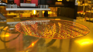
Scalable Metal Oxide Nano Inks for High-Performance Organic, Perovskite, and Thin Film Photovoltaics and OLEDs
#PerovskiteSolarCells #OLED #OrganicPV #PrintedElectronics #NanoInks #ElectronTransportLayer #FlexibleElectronics #Optoelectronics #RollToRoll #SmartMaterials #EnergyTech #SolarInnovation #DisplayTechnology #NextGenMaterials #SustainableElectronics
Author: Maryam Bari & Ashwani Jain PINA CREATION Unlocking printable, low-temperature charge transport layers for next-generation optoelectronics As next-generation optoelectronic technologies—such as Perovskite solar cells (PSCs), OLED displays, and Organic photovoltaics (OPVs) —move from lab to large-scale manufacturing, the pressure is on to find materials that are not only high-performing, but scalable, stable, and compatible with printed device architectures . A critical bottleneck remains the Electron Transport Layer (ETL) and Hole Transport Layer (HTL) . For technologies relying on delicate or flexible substrates, traditional materials such as Organic Semiconductors and traditional metal oxide inks pose serious limitations. High-temperature processing, moisture sensitivity, high cost, and limited lifetime all threaten the viability of commercial deployment. At PINA Creation , we’ve developed a line of ready-to-use SnO₂, NiO and ZnO nano inks that overcome these barriers and unlock practical, large-area fabrication for flexible and rigid optoelectronics. We are Exhibiting in Berlin. Visit our booth at the TechBlick Perovskite Connect event co-located with the Future of Electronics RESHAPED on 22-23 Oc...

28 August 2025
Introducing the full Perovskite Connect 2025 conference program
Perovskite Connect conference and exhibition | 22 & 23 OCT 2025, ECC, Berlin | Co-located with the Future of Electronics RESHAPED Berlin 2025 Perovskite Connect 2025 is shaping up to be the must-attend event for the perovskite industry , bringing together leading innovators, researchers, and manufacturers from across the globe. Taking place on 22–23 October 2025 at the ECC in Berlin , this specialist conference will run alongside the flagship Future of Electronics RESHAPED show. This article highlights some of the key talks that will take place during this conference. Explore the Full Agenda and Register before 12 September 2025 for the best rates Oxford PV – Edward Crossland presents the world’s first commercial perovskite-silicon tandem module . Breaking silicon’s efficiency limits, tandem technology delivers higher performance with minimal changes to existing production lines. The talk highlights Oxford PV’s milestone 2024 shipment, recent advances, and solutions for durability, scalability, and environmental compliance, demonstrating readiness for large-scale deployment. Hangzhou Microquanta Semiconductor – Yang Chen discusses the commercial readiness of perovskite PV . Drawing on lessons from industrial validation and field deployment, the talk addresses solutions to challenges in stability, efficiency, and scalable manufacturing. Insights into certification and real-world testing show how perovskite PV is evolving into a commercially viable alternative to s...