


6 November 2023
TechBlick - The Future of Electronics RESHAPED Event - Finally We Go To The US!
TechBlick, the leading platform for emerging technologies has announced that it will hold a US edition of its very successful 'The Future of Electronics RESHAPED' conference and exhibition in Boston on 12 & 13 June, 2024.
TechBlick is responding to huge demand by the global industry to hold this event. It will be the most important industry and research meeting in this field in the US and the first event for a number of years to bring the entire ecosystem together.
The Future of Electronics RESHAPED conference and exhibition will focus on additive, sustainable, flexible, hybrid, wearable, structural and 3D electronics. As well as a world-class agenda and exhibition, the event will also feature expert-led masterclasses and company tours to some of the innovative organisations in the Boston area.
Khasha Ghaffarzadeh, CEO of TechBlick reported "Following the success of our recent Berlin Event a couple of weeks ago which saw a 50% growth both in attendee and exhibitor numbers, we feel confident that we can hold a successful US event. Indeed we have had such strong exhibitor interest that we have already had to add extra exhibition space. For further information visit https://www.techblick.com/electronicsreshapedusa
Join the global industry at the long-awaited TechBlick US event on 12 & 13 June 2024 in Boston and also in Berlin on 23 & 24 October 2024....

27 October 2023
Simple Fluidic Self Assembly (FSA) Mass Transfer for Low Cost MicroLED Displays | eLux
MicroLED are the ultimate display technology, but the grand challenge of mass transfer at low cost and high yield with variable pixel pitch and no mura effect remains an important theme. On 29-30 NOV 2023, JJ Lee from eLux, Inc. will present at www.MicroLEDConnect.com on their novel simple fluidic self-assembly (FAS) mass transfer process, which positions each µLED by capture of the device in a well structure that also contains the connecting electrodes. This process uses gravity to trap µLED
✅ Simple µLED and substrate structures, recyclable µLED after FSA, and extremely simple and scalable FSA tools. ✅ Handle µLEDs sized from 5 to 200 µm offering flexibility to make a wide variety of displays with resolutions from 400 to 10 ppi or larger.
✅ Assembly speed as high as tens of millions µLEDs per hour on large panels.
✅ µLED emitter area to µLED size ratio adjustable ✅ Fluidic assembly applies relatively low force on the device so brittle materials such as red µLEDs fabricated from AlGaInP can be assembled in the same way as blue and green emitting GaN µLEDs.
Slide [1] shows the progress from LED wafer to uLED array, offering also information on eutectic bonding of TFTs and uLEDs as well as on yield, de-trap, orientation control parameters Slide [2] shows how select harvest of known-good dies as well as randomization in the ink ensure that FAS has low defectivity and no stamp mura. The mura from pick-and-place solution is very clear, resulting from wavelength and l...

27 October 2023
Towards Integrated CMOS+GaN microDisplays fabricated at wafer scale
Future of MicroLEDs: wafer level integration combining III-V devices with CMOS transistors to achieve truly monolithic microdisplay? Daniel Lepkowski and Kenneth Lee from nsc (New Silicon Corp) will join https://www.microledconnect.com/ on 29-30 NOV 2023 to explain how they are enabling and progressing technology.
Slide [2] shows the approach to front-end heterogeneous integration enabling wafer-scale CMOS+GaN LED systems. First the circuit is designed using CMOS EDA tools running a custom nsc PDK that allows designers to layout, simulate, and iterate CMOS + LED circuits like never before. Then during the tapeout phase, the CMOS front end is produced using a properly suited 200 mm CMOS process at one of many established CMOS foundries. This front-end CMOS wafer is then integrated with an as-grown GaN-on-Si wafer using a proprietary double layer transfer technique. The wafer is then returned to the foundry where LED devices are fabricated and interconnected with CMOS devices using standard CMOS back-end processes. This enables higher interconnect densities and greater manufacturability than is possible using traditional hybrid bonding schemes.
Slide [3] shows how they have achieved this on a 200 mm silicon manufacturing line. The device cross section shows how the heterogeneous integration of CMOS and GaN-on-Si looks like on a 200mm Si wafer.
Slide [4] also shows how this integration technique can increase reliability, yield and design freedom of packaging and bondin...

26 October 2023
Fine-Pitch Direct Die Attach Without Thermal Compression | SunRay Scientific
Andrew Stemmerman & John Yundt SunRay Scientific Inc. Eatontown, NJ USA andrew@sunrayscientific.com johny@sunrayscientific.com SunRay Scientific of Eatontown, NJ, USA has developed a new and innovative approach to electronic component assembly. This article will outline the developments of this technology and show examples of this magnetically aligned Anisotropic Conductive Epoxy packaging method used on various substrates. Progress will be shared for dense and fine pitch Land Grid Arrays (LGA) on a semi-rigid interposer. Introduction Flip-chip die and die-to-die bonding, from dense to fine pitch, typically require solder balls and underfills. Underfill and/or edge encapsulant is often utilized to provide additional mechanical strength and stress reduction. The result is a complex assembly process flow. Localized placement of Anisotropic Conductive Adhesive (ACA) or Anisotropic Conductive Film (ACF) for specific components typically involves the fine-pitchuse of thermocompression bonding, an additional process step that could also be damaging to thin silicon. Another drawback for traditional interconnect materials is relatively slow processes, limiting the utility of such technologies. Development towards a wafer scale compatible packaging method will be shared, using a pressure-less and low-temperature magnetically aligned Anisotropic Conductive Epoxy (ACE). Figure 1. Flip Chip assembly comparisons: traditional solder balls & underfill attachment (Left); Die attach with z-ax...


27 October 2023
Total Solution for Mass Production of MicroLED Displays | Toray Engineering
How can equipment manufacturers innovate to meet current and future needs of microLED production? You can join us on 29-30 NOV 2023 at https://www.microledconnect.com/ where Katsumi Araki from Toray Engineering Co., Ltd. will present how they are addressing some of these challenges including 1] Handling of ever smaller microLED die with a stable process: as you can see in slide #2, dies size have shrunk and will continue to do so. To give a sense of the transition consider that a traditional LED is >1mm wherea a microLED die can be less than 2um, a shrinkage of 500-1000 times! This require innovative equipment to handle, to transfer, to bond, to inspect, to repair, etc with near perfect yield 2] Efficient repair process: this is a vital challenge in the industry. To highlight the scale of the challenge, as shown in slide 2, consider a 4mm smart watch. This watch will include 500,000 microLED chips. Thus, a 1% defect will translate into 5000 repair tasks, which would take 7 hours with a standard pick-and-place machine. Or consider a 4k TV. This would have 25M chips and thus at 1% defect rate 250000 chips would need to be repaired, translating to 347 hours with a conventional pick-and-place machine 3] Minimizing image discoloration: when mass transfer is performed using the conventional method (e.g., stamp), uneven brightness and wavelenght are transferred as they. This will need to be addressed In slide [3] you can see the entire process chain from LED chip manufacutring to wa...
27 October 2023
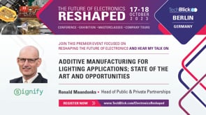
Additive manufacturing for lighting applications; state of the art and opportunities | Signify
In this presentation, Ronald Maandonks will elaborate on Signify's efforts to drive the transition from a linear to a circular economy. He will highlight the significant advantages that technologies like additive manufacturing bring to customers, with a particular focus on 3D printed luminaires. These luminaires are purposefully designed to cater to specific needs and applications across various sectors. Whether it's achieving performance enhancements with higher efficacies in lumen per watt (lm/W) or delivering superior light quality, meeting diverse aesthetic preferences through different colors, textures, or shapes, or enabling seamless system upgrades, the modular concept lies at the heart of addressing these requirements. By allowing for the exchange or addition of modules, this approach not only preserves the value of the product but also minimizes waste, leading to a substantial reduction in CO2 emissions. Furthermore, this innovative method enhances local production capabilities, empowering the ability to manufacture where the products are sold. Overall, the presentation will shed light on Signify's commitment to sustainability, CO2 reduction, and waste reduction through its transformative approach to lighting solutions. SAVE THE DATE...

26 October 2023
Additive Manufacturing for Future High Volume Manufacturing of Electronic Devices | Meta
Recent advances in Additive Manufacturing (or 2D and 3D Print) have poised many of these technologies to displace or augment traditional electronics manufacturing methods, yet significant further advances are still needed in order to obtain broad adoption for high-volume manufacturing of electronics devices. After presenting a view of how additive manufacturing methods could be leveraged for wearable AR/VR devices as well as highlighting the benefits of additive methods, I will dig into key areas where significant developments are still needed, including: component-level and device reliability; design tools; close-loop in-situ process monitoring; integrated manufacturing workflows; productivity and yield; and material properties. I will then conclude with a few application examples, highlighting unique solutions promised by additive methods as well as gaps which remain. SAVE THE DATE...