


6 January 2026
Blackleaf | Water-Based Graphene Inks: A Sustainable Innovation for Thermal Heating Elements
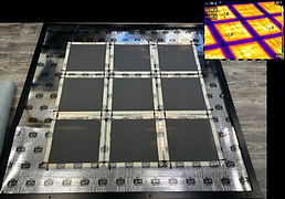
Authors: Anaghim Nasri, R&D Engineer Quentin Maerklen, Process Engineer Water-based graphene inks are emerging as a groundbreaking solution for next-generation heating technology. By leveraging graphene’s exceptional thermal and electrical conductivity, these inks enable thin, flexible heating elements that deliver high heat output with minimal power. Importantly, sustainability is becoming a key market driver, with growing demand for water-based, responsibly sourced graphene inks as eco-friendly alternatives to metal-based conductive materials. This article explores how water-based graphene inks provide efficient and uniform heating, their environmental advantages over conventional carbon-based inks, and the role of Blackleaf in driving this innovation forward. As the demand grows for eco-friendly heating (from automotive seats to building systems), water-based graphene inks offer a powerful combination of performance, sustainability, and scalability. Introduction: Blackleaf Inks for Next-Generation Heating One of the pioneers bringing this technology to market is Blackleaf, a French graphene manufacturer and ink developer. Blackleaf has positioned itself as a leading producer of graphene and formulated inks in Europe, with a capacity of over 120 tons per year of graphene products by 2027, all produced in-house in France. Blackleaf’s product portfolio includes ready-to-use graphene conductive inks for a variety of uses. Notably, the company has focused on graphene-base...

24 November 2025
The Future of Electronics RESHAPED USA
Conference & Exhibition: 10 & 11 June 2026 | Masterclasses: 9 June 2026 Computer History Museum, Mountain View, California, USA Co-located with the Nextflex Innovation Day Exhibition spaces 75% sold already! Super early bird rate expiring 19 DEC 2025 The next Future of Electronics RESHAPED USA show will move from the East Coast to the West Coast, taking place at the iconic Computer History Museum in Mountain View, California! Let's RESHAPE the Future of Electronics together, one layer at a time, on 10 & 11 June 2026 in Mountain View, making it Additive, Printed, Sustainable, Flexible, Hybrid, Stretchable, Wearable, Textile, Structural, 3D... Global Agenda Discover key breakthroughs RESHAPING the future of electronics. Discover more here The TechBlick team is currently curating the agenda. To get a sense of the calibre of our events, please explore all our previous events here. All these past events across all locations, technology topics and years are also available to you with your annual pass. Super early bird attendee rates end on 19 DEC 2025. Secure your spot now Incredible Tradeshow
Experience the innovations that will RESHAPE electronics
Explore
75+ exhibitors will be joining us onsite, creating a vibrant tradeshow floor that reflects the state-of-the-art across the entire global value chain for additive, printed, hybrid, sustainable, wearable and 3D electronics. The exhibition floor is already 75% full. Please secure your space now. Learn more and download the pac...

17 October 2025
LevSurf™: A Technical Evolution in 3D-Formable Hard-Coated Films
LevSurf™ is a UV‑cured hard-coated polycarbonate (PC) film engineered to enable three-dimensional forming for IMD/FIM manufacturing — combining scratch resistance and robust chemical durability with material flexibility. The coating is fully cured prior to forming, eliminating the need for post-processing steps like secondary UV curing or lacquer, increasing throughput and reducing defect rates. Tailored for cover-lens substitution in high-resolution displays (e.g. automotive instrument panels), LevSurf offers optical clarity comparable to glass, with weight savings and potential reductions in CO₂ footprint per vehicle lifecycle. Constructed using polycarbonate substrate, LevSurf features anti-reflective (F18) or glossy (F04) finishes, each optimized for display readability or aesthetic effect. The hardcoat layer yields durability — pencil hardness H and full chemical resistance while allowing elongation of up to ~125% during forming without cracking. The film maintains excellent optical performance, with haze as low as ~0.1% and reflectance around 1.4%, paired with anti-fingerprint and anti-glare finishes for improved visual performance. Kimoto applies the UV-curable coating using ISO‑certified clean‑room R2R coating lines, ensuring minimal particulate contamination for high-resolution display optics. After coating, the film can be printed (e.g. for in-mold graphics), then formed via IMD/FIM tooling. As the coating is fully cured, there’s no post-curing required — meaning lo...

17 October 2025
ZnO Deposition with Direct Atomic Layer Processing (DALP®)
Authors: Laszlo Izso. Matthias Carnoy. Nandan Singh Ruhela. Benjamin Borie. Mira Baraket. Maksym Plakhotnyuk Introduction: ZnO from an Applications point of view Zinc oxide (ZnO) is a versatile semiconductor material that has attracted broad interest in electronics and sensing. It features a direct wide bandgap of ~3.37 eV, making it useful for UV optoelectronic devices like LEDs and photodetectors [1]. ZnO is also abundant, low-cost, and chemically stable, and it can be synthesized via relatively easy methods all contributing to its popularity in research and industry [2]. Beyond optics, ZnO can be doped to achieve high conductivity (transparent conducting films) and used in thin-film transistors (TFTs) as an n-type semiconductor channel. In microelectronics, ZnO and related oxides have been explored for transparent and flexible transistors, as well as varistors and UV sensors. Its wurtzite crystal structure lacks inversion symmetry, giving ZnO a strong electromechanical coupling it is one of the few semiconductors that is also piezoelectric [3]. This means mechanical strain can induce an electric charge and vice versa, enabling ZnO to serve in mechanical actuators and sensors [3]. In MEMS/NEMS devices, polycrystalline ZnO thin films (often c-axis oriented) are used for piezoelectric actuators, micro-resonators, and energy harvesters. For example, ZnO thin films form the active layer in surface acoustic wave (SAW) devices and bulk acoustic resonators for filters and sensors ...

4 December 2025
Voltera | Enabling Multilayer Flexible PCBs with Direct Ink Writing Technology
Author: Jesus Zozaya, CEO, Voltera, sales@voltera.io
It was our pleasure to present a masterclass at TechBlick Berlin on advancements in printed electronics prototyping. As a follow-up, we’d like to share an example of a multilayer flexible circuit we printed on PET. To watch this presentation in full, please purchase TechBlick Annual Pass at https://www.techblick.com/registration and login to TechBlick platform https://app.swapcard.com/event/techblick
MATERIALS USED Voltera Conductor 3 silver ink ACI Materials FS0142 Semi-Sintering Conductive Ink ACI Materials SI3104 Stretchable Printed Insulator Voltera T4 solder paste Voltera solder wire Siraya Tech Tenacious Flexible Resin SUBSTRATES USED Normandy Coating polyethylene terephthalate (PET) FR1 board TOOLS AND ACCESSORIES V-One PCB printer NOVA materials dispensing system Voltera disposable nozzle Nordson EFD 7018395 dispensing tip Nordson EFD 7018424 dispensing tip Nordson general purpose dispense tips NE555DR timer LEDs Project Overview Purpose The goal of this project was to prototype a flexible multilayer LED wheel roulette circuit that was traditionally considered rigid and validate the redesign of the circuit. Design This project involves a multilayer flexible PCB for the LED roulette circuit and a traditional control board that powers it. We adapted the design of an LED roulette circuit, originally developed for a 3” × 4” FR4 board by ITIZ, Voltera’s authorized reseller in Korea. This new version is printed on ...

17 October 2025
Building the Future of Electronics: Brewer Science’s Material Innovations for Additive Manufacturing
As electronics demand greater miniaturization, multifunctionality, and integration, the materials enabling these advancements require significant consideration. Brewer Science is pioneering a new frontier in additive electronics by developing advanced functional materials, including printable low-loss dielectrics, encapsulants, and optical layers, that empower high-performance sensor systems and advanced packaging solutions. These innovations not only enhance device capabilities but also strengthen the domestic electronics supply chain, positioning the U.S. as a leader in next-generation electronics manufacturing. The Challenge: Evolving Demands in Electronics Manufacturing Microelectronics manufacturing has long relied on proven techniques like photolithography and PCB fabrication, technologies that have enabled decades of innovation and remain essential to many high-performance applications. However, as the industry pushes toward greater miniaturization, multifunctionality, and integration, new manufacturing paradigms are emerging to meet these evolving demands. Additive manufacturing offers unique advantages in design flexibility, rapid prototyping, and integration of complex 3D structures. Yet, while structural additive manufacturing has matured, the development of functional materials, such as printable dielectrics, conductive materials, and encapsulants, remains a critical frontier. Brewer Science is helping bridge this gap by introducing advanced materials that compl...

17 October 2025
Empowering the Future of Industrial Printed Electronics
Digital Additive Hybrid Solutions as a Value Driver
Authors: Frédéric SOULIER and Viktoriya TESSIER-DOYEN Email authors here In the era of Smart Factories, IoT, AI and Sustainability Goals, the electronics and industrial sectors are undergoing a profound transformation. Traditional subtractive methods : etching, photolithography, plating still dominate, but they come with high fixed tooling cost, lead times, and material wastage. Digital Additive Manufacturing — particularly in the domain of Printed Electronics — is emerging as a powerful disruptive lever. Among various solutions in this space, the CeraPrinter, by Ceradrop - MGI Group, offers hybrid digital deposition equipment that combine multiple printing technologies : Inkjet, NanoJet, Aerosol Jet®, Microdispensing to deliver flexible, precise, and sustainable manufacturing across industrial domains. This article discusses key trends, technical merits, hybrid approaches, and business advantages of digital additive hybrid manufacturing. We are Exhibiting in Berlin. Visit our booth at the TechBlick event on 22-23 October 2025 in Berlin. Contact us for your special discount coupon to attend Trends & Growth in the Printed Electronics Sector The global printed electronics market is forecast to grow strongly — expected to nearly double by 2030. This expansion is driven by flexible, lightweight, multifunctional electronics for wearables, automotive, sensors, and IoT devices.Key trends include flexibility, sustainability, on-...

16 October 2025
Rethinking PCB manufacturing: A digital and sustainable approach
Contact: Max Scherf, Maximilian.Scherf@profactor.at Reimagining the entire life-cycle of electronics—from raw material sourcing to end-of-life management—is essential for building a sustainable economy and society. The EU-funded HyPELignum project addresses this challenge by exploring a holistic approach for manufacturing electronics with net zero carbon emissions, centred around additive manufacturing and wood-derived materials. Methodology Materials By creating novel materials derived from wood feedstock, such as lignocellulosic composite boards, bio-derived resins, and functional compounds incorporating abundant, low-impact metals, a transition towards green electronics can be realized. These new materials expand the technological possibilities for electronics while maintaining a strong focus on environmental responsibility. A key material in this development is Cellulose Nano Fibrils (CNF), known for its excellent mechanical performance, ease of application, biodegradability, and eco-friendly nature. CNF has emerged as a promising material for eco-electronics due to its unique properties. Initial research at Empa demonstrated the feasibility of using CNF from delignified pulp (ECF) for eco-electronics applications. The prepared CNF samples exhibited robust mechanical strength and stability in indoor environments, providing a strong foundation for further development. While CNF-based ecoPCBs show strong mechanical properties comparable to FR4 PCBs, they face challeng...