Search Results
Search this site
1075 results found with an empty search
- Evolution of flexible active matric backplanes to integrate all side circuits and driving ICs?
Here, Meike Baumgarten explains how InnovationLab GmbH is evolving the architecture of flexible active matrix backplanes with printed electronics and thinned ICs as part of 2-Horisons project to eliminate all rigid parts. In a conventional set up, the non-pixel-level circuits as well as driver IC sit off-site, linked with the flexible backplane via some connector. In this project, iL has already demonstrated that it can print many of the circuit functions (e.g., multiplexers, decoders) already onto the flexible backplane sheet. This is an important advancement of the technology. The next step of the evolution will be to print also full circuits and fan-outs and place thinned silicon IC/dies onto the flexible active matrix backplane sheet, thus integrating all the electronics into the backplane sheet itself. This is essential for creating very flexible displays and will be an important development in the field. To support this project, and also to generally support flexible hybrid electronics, iL is also developing techniques to solder ICs and SMDs directly onto the substrate with printed metallization. Here, Cu inks are S2S printed to, for example, form NFC on substrates such as PEN, FR4, and PET. Given the non-bulk conductivity of inks, a high dry thickness of 30um is required for printed Cu metallization, which can result in spreading and thus shorting between the pins of ICs. Meike Baumgarten explains various approaches to overcome this challenge To learn more join the Printed Electronics community in Eindhoven, the Netherlands, on 12-13 OCT 2022. For more information please visit https://www.techblick.com/electronicsreshaped Dr. Florian UllrichDr. Christoph KaiserInnovationLab GmbH #printedelectronics#flexibledisplays#backplanes#tft#solder#smt
- Standard printing to securely bridge the gap between physical and digital worlds?
PRISMADE LABS has developed an innovative technology to enable this. They use standard printing machinery with carbon inks to print conductive patterns on almost any substrate (PC, PET, Paper, etc). These conductive patterns act as “touch transformers” converting an input touch signal into a unique signal pattern or signature, which is then read and recognized by a touch sensor like a mobile phone. The unique signal can then authenticate a card or a product or act as a secure trigger between physical and digital world. The compatibility with standard printing techniques makes this approach widely adoptable in almost any sector where printing is used. The lack of electronic parts, unlike NFC or RIFD tags, makes it lower cost and also environmentally friender, especially in high volume and disposable applications The technology sits somewhere between a simple low-cost but unsecure QD code and an expensive but secure electronic recognition system There have already been many examples of commercial success and demonstration including in driving licenses, in marketing compaigns, and in securing bockchain-link collectables, etc In one interesting example (May 2021), Prismade discuss how it enables the Twich streaming community to security print the physical twin of the their unique digital cards (note: the digital cards can be designed by a member of the Twitch community who has earned enough points). There were, according to Prismade, some 50M digital cards designed by May 2021 For more info about printed electronics join TechBlick on 12-13OCT2022 in the Netherlands https://www.techblick.com/electronicsreshaped
- Solderable "silver" conductive paste for hybrid electronics compatible with SMT assembly?
Curable silver inks with millisecond curing for rapid R2R printing? In this short 5-min video by Philipp Hoelzl you will learn about both these trends. In particular you will see the following: Solderable Silver Ink: Elantas has developed a silver ink which is resistant up to 200C and compatible with substrates like Kapton. This ink- offering <15 mOhm/s/mill- survives harsh conditions, meaning that it can - together with printable high-T insulators - enable temperature sensors for environments in which inks normally burn! Interestingly, the high temperature nature means that it can also be soldered. Here, you will see prototypes by Kundisch GmbH & Co. KG showing how these silver conductive pastes can be soldered using a low-temperature Sn-Bi-Ag solder with a eutectic temperature of 138C. Here you will see a complex example involving soldered LEDs, NFC function, and touch screen elements with printed metallization on glass. This is an important development because it shows that not only copper inks, but also silver conductive inks can also be soldered, thereby enabling SMT assembly of parts and thus enabling flexible hybrid electronics R2R Silver Conductive Inks: R2R printing is all about speed. Often, the heat curing step (a few min in the oven at >120C) slows the entire process down, and requires long ovens with buffer zones. This is why UV curable inks are desired. However, many UV inks do not meet requirements, especially as the absence of forceful drying, unlike heat curing, may mean that particles do not pull together to form a highly conductive line. Here, Philipp Hoelzl introduces a UV curable ink able to reach <30mOhm/sq/mill conductivity with a low VoC content (<2%) with sub-second curing via UV exposure To learn more and to meet the ELANTAS EUROPE team join the global community in Eindhoven, Netherlands on 12-13 OCT 2022 Curable silver inks with millisecond curing for rapid R2R printing? In this short 5-min video by Philipp Hoelzl you will learn about both these trends. In particular you will see the following: Solderable Silver Ink: Elantas has developed a silver ink which is resistant up to 200C and compatible with substrates like Kapton. This ink- offering <15 mOhm/s/mill- survives harsh conditions, meaning that it can - together with printable high-T insulators - enable temperature sensors for environments in which inks normally burn! Interestingly, the high temperature nature means that it can also be soldered. Here, you will see prototypes by Kundisch GmbH & Co. KG showing how these silver conductive pastes can be soldered using a low-temperature Sn-Bi-Ag solder with a eutectic temperature of 138C. Here you will see a complex example involving soldered LEDs, NFC function, and touch screen elements with printed metallization on glass. This is an important development because it shows that not only copper inks, but also silver conductive inks can also be soldered, thereby enabling SMT assembly of parts and thus enabling flexible hybrid electronics R2R Silver Conductive Inks: R2R printing is all about speed. Often, the heat curing step (a few min in the oven at >120C) slows the entire process down, and requires long ovens with buffer zones. This is why UV curable inks are desired. However, many UV inks do not meet requirements, especially as the absence of forceful drying, unlike heat curing, may mean that particles do not pull together to form a highly conductive line. Here, Philipp Hoelzl introduces a UV curable ink able to reach <30mOhm/sq/mill conductivity with a low VoC content (<2%) with sub-second curing via UV exposure To learn more and to meet the ELANTAS EUROPE team join the global community in Eindhoven, Netherlands on 12-13 OCT 2022 Curable silver inks with millisecond curing for rapid R2R printing? In this short 5-min video by Philipp Hoelzl you will learn about both these trends. In particular you will see the following: Solderable Silver Ink: Elantas has developed a silver ink which is resistant up to 200C and compatible with substrates like Kapton. This ink- offering <15 mOhm/s/mill- survives harsh conditions, meaning that it can - together with printable high-T insulators - enable temperature sensors for environments in which inks normally burn! Interestingly, the high temperature nature means that it can also be soldered. Here, you will see prototypes by Kundisch GmbH & Co. KG showing how these silver conductive pastes can be soldered using a low-temperature Sn-Bi-Ag solder with a eutectic temperature of 138C. Here you will see a complex example involving soldered LEDs, NFC function, and touch screen elements with printed metallization on glass. This is an important development because it shows that not only copper inks, but also silver conductive inks can also be soldered, thereby enabling SMT assembly of parts and thus enabling flexible hybrid electronics R2R Silver Conductive Inks: R2R printing is all about speed. Often, the heat curing step (a few min in the oven at >120C) slows the entire process down, and requires long ovens with buffer zones. This is why UV curable inks are desired. However, many UV inks do not meet requirements, especially as the absence of forceful drying, unlike heat curing, may mean that particles do not pull together to form a highly conductive line. Here, Philipp Hoelzl introduces a UV curable ink able to reach <30mOhm/sq/mill conductivity with a low VoC content (<2%) with sub-second curing via UV exposure To learn more and to meet the ELANTAS EUROPE team join the global community in Eindhoven, Netherlands on 12-13 OCT 2022 https://www.techblick.com/electronicsreshaped
- Reinventing the Wheel? Printing (R)Evolution For A Luxury Brand
Speaker: Rafael Michalczuk | Company: SWAROVSKI| Date: 10-11 March 2021 | Full Presentation Swarovski is innovating since decades in the additive manufacturing domain and printing technologies form an important puzzle piece in the manufacturing processes. But is it now time to reinvent Gutenberg´s invention? As proof-of-concept Swarovski will showcase in the talk different innovations – ranging from additive manufacturing in jewelry, 3D glass printing to 2D/3D printed electronics applications and nano-imprint lithography in various application areas for the luxury brand. Rafael Michalczuk Senior Technology & Funding Manager @ SWAROVSKI Bio Rafael Michalczuk, Senior Technology & Funding Manager at Swarovski, is supporting research, development and innovation projects within interdisciplinary and cross-functional teams at Swarovski, especially with key enabling technologies involved (e.g. additive manufacturing, printed electronics, artificial intelligence, robotics). Additionally he is founder of the innovation & funding consulting agency InnoPotentials. In this capacity he serves a broad portfolio of clients (from startups, SMEs to large companies and R&D institutions) to develop innovative business ideas, secure funding and support the overall innovation journey of the customers. Join TechBlick on an annual pass to join all live online conference or online version of onsite conference access library of on-demand talks (600 talks + PDFs) portfolio of expert led masterclass year-round platform https://www.techblick.com/ And do NOT miss our flagship event in Berlin on 17-18 OCT 2023 focused on Reshaping the Future of Electronics. This event attracts 550-600 participants from all the world and offers a superb ambience and dynamic exhibition floor. To learn more visit https://www.techblick.com/electronicsreshaped To see feedback about previous event see https://www.techblick.com/events-agenda
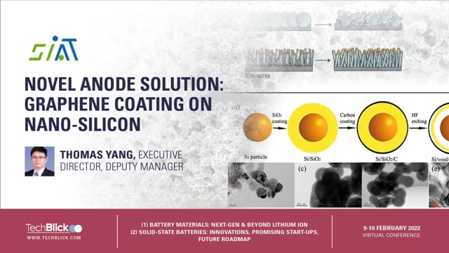
- Novel anode solution: graphene coating on nano silicon
Speaker: Thomas Yang | Company: Sino Applied Technology | Date: 9-10 Feb 2022 | Full Presentation Join TechBlick on an annual pass to join all live online conference or online version of onsite conference access library of on-demand talks (600 talks + PDFs) portfolio of expert led masterclass year-round platform https://www.techblick.com/ Our next battery-related event will take place on 15-16 FEB 2023, covering 1) Solid-State Batteries: Innovations, Promising Start-Ups, & Future Roadmap 2) Battery Materials: Next-Generation & Beyond Lithium Ion The speakers include: General Motors, Graphenix Development, Brookhaven National Laboratory, Fraunhofer IKTS, RWTH Aachen University, Lawrence Livermore National Laboratories, Meta Materials Inc, Skeleton Technologies, Solid State Battery Inc, Argonne National Laboratories, OneD Battery Sciences, VTT, Leyden Jar Technologies B.V., b-Science, Rho Motion, Wevo-Chemie, LiNA Energy, CNM Technologies, Ionblox, Empa, Zinc8 Energy Solutions, Avicenne Energy, Echiontech, South8 Technologies, Basquevolt, NanoXplore, Chasm, Li Metal, Sila Nanotechnologies, Quantumscape (tentative), Fraunhofer ISI, etc https://www.techblick.com/
- How to screen print sub 30um features?
Screen printing never ceases to advance and is entering into ultrafine line printing territory. FERNANDO ZICARELLI explains in this short 5-min talks important considerations to achieve fineline printing and further push the resolution down: - Team effort: screen printing is a team effort, requiring close collaboration between paste maker, mesh and emulsion maker, printer, etc. - Black stainless steel mesh: conventional stainless steel meshes are reflective (10-15%). To achieve narrow and sharp openings in the high resolution photosensitive emulsion, random reflections from the stainless steel mesh- especially at 365nm and 405nm wavelengths- need to be minimized. This is why a black version is required - Narrow meshes: Asada Mesh is the master of making the most advanced stainless steel meshes. To achieve sub 30um, a mesh with a diameter of 11-13um with 55%-60% opening will be required. Asada Mesh is already pushing the performance envelope, offering even 9um meshes. This is an incredible advance, considering it takes around 3 years of intense developments to shave 1um from the diameter of the mesh Substrate selection: depending on paste, substrate selection is key to balance surface tension/energy. Here, Fernando shows the outsize impact of substrate properties on on even 50um printed lines To learn more and to meet the Asada Mesh team join us in Eindhoven (12-13 OCT) https://www.techblick.com/electronicsreshaped
- Ink-Free Digital Printing | Solder/Adhesive Free Die Bonding | Roadmap for 3DPE | HTL for ...
Ink-Free Digital Printing | Solder/Adhesive Free Die Bonding | Roadmap for 3DPE | HTL for High Performance OPV | OTFTs compatible with LCD ProductionHigh-Performance Before delving into the details of the technology updates for this week, I would like to say that we very excited about our onsite event in Eindhoven, the Netherlands, on 12-13 OCT 2022. The exhibition is long sold out with a long waiting queue, the world-class agenda is announced, and there is very high demand for attendee tickets. You can see the full information here. This is the most important upcoming event in the industry. Next, we will provide updates and insights on a few interesting developments in the world of additive electronics. We will cover (1) dry ink-free digital printing (2) HTL with deep work function (3) roadmap for 3DPE (4) direct die bonding on paper with solder or adhesives (5) liquid wire based on Ga-In-Sn conductive gels (5) OTFT backplanes compatible with LCD production and (6) key steps in printing sub 30um linewidths A dry ink-free digital printing process to deposit multifunctional materials? We recently came across this interesting system, developed by Masoud Mahjouri-Samani, PhD et al Auburn University. Here, as shown below, an excimer laser is focused by lens onto a target. The target is ablated, forming a plume of nanoparticles which then condense onto the substrate to form nanoparticles. The laser system can be used to in situ sinter and crystallize the structure. This dry printing process thus involves no inks and can 'print' complex multifunctional materials like TiO2 or ITO, going beyond the capability of traditional digital ink printing. These researchers claim that this "new method allows the in situ and on-demand formation of various nanoparticle building blocks in atmospheric pressure and at room temperature. These nanoparticle building blocks can be directed toward the substrate through a nozzle forming a stream of nanoparticles that can be laser sintered/crystallized on various substrates in real-time." Indeed, below you can see an example of the generated and sintered TiO2 nanoparticles. Furthermore, you can see examples of ITO and TiO2 circuits printed on SiO2 substrate using this process. This is a novel, promising and innovative approach to direct digital deposition of a wide range of materials on various substrates. It may overcome some key limitations of ink-based wet printing techniques, especially in terms of possible material options. Of course, This is currently a small-scale lab operation and of course, as technology development advances more trade-offs will become known. The technology is now entering the commercialization phase. Indeed, NanoPrintek (NanoPrintek, Inc.) has been recently set up to take this exciting approach forward. New HTL materials enable bridging the gap between the latest lab-level and production-level printed OPV performance. Below you can see the historical rise of OPV (organic photovoltaics) efficiencies from 2.5% in 2000 to >18% now, showing how evolution in materials has driven this rise. (Material Evolution: P3HT: PCBM --> emergence of push-pull polymers (PPP) --> rise of non-fullerene acceptors (NFAs)---> novel PPP and NFA). The chart below, by Nicolas Bouchard Brilliant Matters, also reveals the large gap between the best lab results and the best production level results with the highest industry-scale results being <8% !! One key factor holding back the efficiency of production-level OPVs is the unavailability of a hole transport layer (HTL) compatible with the latest OPV donor and acceptor materials. This is because the latest novel donor and acceptor materials have wider bandgaps, thereby creating a large energy barrier with the common traditional HTL materials: PEDOT. This acts against charge injection and lowers efficiency. Thus, to get the best from the latest PPPs and NFAs in industry-scale processes, one requires an HTL material in a non-halogenated solvent with a deep work function which can be printed in ambient conditions and which yields uniform thick (>100nm) layers. Brilliant Matters has developed such a material. Here, it is shown how this novel printable deep HTL achieves results equivalent to MoO3 (best evaporated material) when used with PTQ10 and NFA. This is an important step in the further development and industrialization of organic photovoltaics You can see a short 5-min presentation by Nicolas Bouchard explaining this in good details here Direct flip chip bonding on paper without adhesive or solder? Ali Roshanghias et al Silicon Austria Labs (SAL) demonstrate an interesting approach in a recent publication, exploiting the unique properties of polypropylene(PP) coatings on paper. Here, the bottom of the dies is coated with a sputtered lines of Cr(10nm)/Au (300nm) layers. The paper is coated with a thin 18-um PP layer through extrusion lamination. Ag tracks were R2R flexoprinted and dried. The dies are simply flip chip thermocompressed into the substrate. The results - shown below- confirm that the bonding is formed without an adhesive or solder layer. Here, the PP layer is softerend at 150C and reflows locally at temperature of 162-165C during die bonding, allowing the bumps to penetrate and make contacts with the printed Ag lines. Upon solidification, the PP layer cirumpassed the contacts, acting essentially as a pre-applied adhesive and applying a compressive force to stabilize the electrical contacts. This is an interesting advancement in the field and an alternative process to solder and ACFs. However, now, the burden is to apply a PP layer in advance. If the PP layer is essential in any case to planarize substrate and/or promote printability, then this step may simplify the process, removing an additional dispense/print step and removing the need for additional materials. The future roadmap of 3D printed electronics in the medium (3-5 year) and long (5-10 year) terms? In this short 5-min presentation, Dr. Martin Hedges shares his insights about the current status as well as medium term (3-5 year) and long term (5-10 year) development roadmap of the industry. Martin is the CEO of Neotech AMT GmbH, a leader in the development of 3D printed electronics machinery, for both prototyping and volume production. Current status: you can exampleds of (1) print on already 3D surfaces and (2) fully additive 3D printed electronics. In the latter, you can see an example of a filament (FFM) 3D printer building the mechanical part. The process is interrupted to automatically do SMT PnP and Ag metal jetting for building the conductive tracks. Here, multiple layers of interconnected electronics are created within the 3D structure, integrating parts such as LED, optics, waveguides, etc Short term (3-5 year) roadmap: the industry should complete the first completely automated processing line based on digital 3D printing of electronics. Some degree of AI/ML will also be integrated for quality inspection and perhaps even auto correction. Furthermore, a wide range of functionalities, especially power electrodes, will be integrated, perhaps using cermaic structures, and the printed area/volume will also expand to form large 3D objects. Long term (5-10year) roadmap: completely new product architectures will be enabled and the industry can start to move away from traditional etching-based PCB production techniques. Furthermore, automated recycling, repair and reuse will be possible How to screen print sub 30um features? Screen printing never ceases to advance and is entering into ultrafine line printing territory. This slideshow and short video considers what is required to reach sub 30um features in production: Team effort: screen printing is a team effort, requiring close collaboration between paste maker, mesh and emulsion maker, printer, etc. Black stainless steel mesh: conventional stainless steel meshes are reflective (10-15%). To achieve narrow and sharp openings in the high resolution photosensitive emulsion, random reflections from the stainless steel mesh- especially at 365nm and 405nm wavelengths- need to be minimized. This is why a black version is required Narrow meshes: Asada Mesh is the master of making the most advanced stainless steel meshes. To achieve sub 30um, a mesh with a diameter of 11-13um with 55%-60% opening will be required. Asada Mesh is already pushing the performance envelope, offering even 9um meshes. This is an incredible advance, considering it takes around 3 years of intense developments to shave 1um from the diameter of the mesh Substrate selection: depending on paste, substrate selection is key to balance surface tension/energy. The examples below, presented by FERNANDO ZICARELLI, show the outsize impact of substrate properties on on even 50um printed lines. You can watch the full video by Fernando here. High-performance TFT backplanes printed at 80C and patterned using existing LCD equipment? It is incredible to see the progress that organic semiconductors (OSC) have made over the past 15-20 years. SmartKem, Inc. is removing the long-existing barriers to adoption of OTFT technology. These are hard-won crucial and essential development steps to ensure commercial success, as technical progress alone in terms of mobility or stability will never suffice. EDA tools: They have designed EDA tools enabling design and simulation of circuits using their OTFT circuits. This is an essential prerequisite for adoption which had been previously missing Full portfolio of TFT materials: TFT is not just the semiconducting layer. All materials in a TFT stack must work together in an optimized way. Some 50M and ten years have been spent to develop a full portfolio of materials required to make an OTFT together with processing parameters including passivation layers, sputter resistant layer, base layer gate insulator, etc. This is incredibly important because all materials must work together and ensure compatibility with existing production processes. Compatibility with existing processes: One can not expect display makers to reinvent the wheel and to adopt not just a new material but also a new process. Thus compatibility with existing processes is an absolute must-have. Smartkem has ensured that one can make OTFT backplane using its material set based on existing LCD equipment Commercial partnerships across various display technologies: They have announced partnerships on AMOLED, QD-LCD displays, and mini-LED with RiT Display, Nanosys, and an unnamed Taiwanese player, respectively. This way they are covering multiple technology areas, and not chasing only a single target market. In the past, this error proved costly as most OTFT developers in the past only banked on low hanging fruit of e-papers! It is a delight for us to see the progress of OTFT technology. The barriers to adoption are being cleared away. In the end, this technology proposes to offer the lowest processing cost for good enough displays, a prerequisite for the ubiquitous adoption of the emerging metaverse! Watch a full 5-min presentation by Ian Jenks by clicking here A full musculoskeletal kinematics platform using ultra-stretchable liquid metals? Gallium-Indium-Tin is an interesting material for stretchable electronics. It can be formed into a non-toxic RoHS-compliant gel and applied to almost any substrate to form stretchable conductive metallizations and circuits. It retains its limited liquidity, meaning that it can follow the form of the substrate as the substrate stretchec, provided the limits of its hysteresis are not approached. In this presentation Jorge Carbo - innovator at Liquid Wire Inc.- shares data showing that they have approached 1M cycles of 100% stretch without any change in resistance- this is some benchmark to beat! In fact, most stretchable inks will struggle to match this performance (although they will likely offer higher conductivity). Furthermore, They are developing a full platform based on its material. As can be seen, this platform integrates their stretchable interconnects together with microprocesses, strain gauge sensors, and other rigid ICs, showing that they can form fully-functional deformable silicone based novel sensor systems with embedded electronics. The slides and the video below also outlines multiple examples of this technology, showing how this 'second skin' forms the basis of a platform technology that can be used in measuring athletic performance, in VR/AR gaming, clinical trials, etc.
- In-mold Electronics Add Context Awareness to Smart Apparel
Speaker: Kimmo Pernu | Company: Movesense by Suunto Oy| Date: 10-11 March 2021 | Full Presentation Movesense is an open sensor platform for creating new solutions to track motion, heart rate and ECG. Movesense is used for building wearable sensor concepts and for integrating sensors with apparel. To enable smooth apparel integration and to provide context information for the sensor, Movesense team of the Finnish sports watch expert Suunto worked together with TactoTek, another Finnish tech company specialized in IME, to develop a flexible connector element that includes in-molded electronics and can be applied to clothing with typical textile industry methods. The presentation describes the project background and steps in practice. Join TechBlick on an annual pass to join all live online conference or online version of onsite conference access library of on-demand talks (600 talks + PDFs) portfolio of expert led masterclass year-round platform https://www.techblick.com/ And do NOT miss our flagship event in Berlin on 17-18 OCT 2023 focused on Reshaping the Future of Electronics. This event attracts 550-600 participants from all the world and offers a superb ambience and dynamic exhibition floor. To learn more visit https://www.techblick.com/electronicsreshaped To see feedback about previous event see https://www.techblick.com/events-agenda
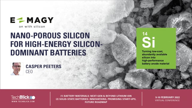
- Nano-porous silicon for high-energy silicon-dominant batteries
Speaker: Casper Peeters | Company: E-Magy | Date: 9-10 Feb 2022 | Full Presentation A major improvement for the next generation of Li-ion batteries is the introduction of silicon as material for the anode, bringing capacity and fast charging to the next level. The biggest challenge of applying silicon-dominant anodes in Li-ion batteries, is silicon's tendency to expand during cycling. E-magy has invented and manufactures micron-sized silicon particles with nanopores that overcome this challenge by containing that expansion within the nanopores themselves. Li-ion batteries with anodes made of E-magy silicon hold 40% more energy than those made of graphite. It's the low-cost, drop-in solution compatible with existing production lines that the EV industry needs – as currently verified by R&D managers of more than a dozen leading automotive and battery manufacturer brands. Join TechBlick on an annual pass to join all live online conference or online version of onsite conference access library of on-demand talks (600 talks + PDFs) portfolio of expert led masterclass year-round platform https://www.techblick.com/ Our next battery-related event will take place on 15-16 FEB 2023, covering 1) Solid-State Batteries: Innovations, Promising Start-Ups, & Future Roadmap 2) Battery Materials: Next-Generation & Beyond Lithium Ion The speakers include: General Motors, Graphenix Development, Brookhaven National Laboratory, Fraunhofer IKTS, RWTH Aachen University, Lawrence Livermore National Laboratories, Meta Materials Inc, Skeleton Technologies, Solid State Battery Inc, Argonne National Laboratories, OneD Battery Sciences, VTT, Leyden Jar Technologies B.V., b-Science, Rho Motion, Wevo-Chemie, LiNA Energy, CNM Technologies, Ionblox, Empa, Zinc8 Energy Solutions, Avicenne Energy, Echiontech, South8 Technologies, Basquevolt, NanoXplore, Chasm, Li Metal, Sila Nanotechnologies, Quantumscape (tentative), Fraunhofer ISI, etc https://www.techblick.com/
- High-performance TFT backplanes printed at 80C and patterned using existing LCD equipment?
It is incredible to see the progress that organic semiconductors (OSC) have made over the past 15-20 years. Ian Jenks, CEO of SmartKem, Inc.- a leader in the field- explains in this short 5-min presentation how they are removing the long-existing barriers to adoption of OTFT technology. These are hard-won crucial and essential development steps to ensure commercial success, as technical progress alone in terms of mobility or stability will never suffice. 1- EDA tools: They have designed EDA tools enabling design and simulation of circuits using their OTFT circuits. This is an essential prerequisite for adoption which had been previously missing 2- Full portfolio of TFT materials: TFT is not just the semiconducting layer. All materials in a TFT stack must work together in an optimized way. Some 50M and ten years have been spent to develop a full portfolio of materials required to make an OTFT together with processing parameters including passivation layers, sputter resistant layer, base layer gate insulator, etc. This is incredibly important because all materials must work together and ensure compatibility with existing production processes. 3- Compatibility with existing processes: One can not expect display makers to reinvent the wheel and to adopt not just a new material but also a new process. Thus compatibility with existing processes is an absolute must-have. Smartkem has ensured that one can make OTFT backplane using its material set based on existing LCD equipment 4- Commercial partnerships across various display technologies: They have announced partnerships on AMOLED, QD-LCD displays, and mini-LED with RiT Display, Nanosys, and an unnamed Taiwanese player, respectively. This way they are covering multiple technology areas, and not chasing only a single target market. In the past, this error proved costly as most in the past banked on e-papers alone for OTFTs. It is a delight for us to see the progress of OTFT technology. The barriers to adoption are being cleared away. In the end, this technology proposes to offer the lowest processing cost for good enough displays, a prerequisite for the ubiquitous adoption of the emerging metaverse!
- A dry ink-free digital printing process to deposit multifunctional materials?
We recently came across this interesting system, developed by Masoud Mahjouri-Samani, PhD et al Auburn University. Here, as shown below, an excimer laser is focused by lens onto a target. The target is ablated, forming a plume of nanoparticles which then condense onto the substrate to form nanoparticles. The laser system can be used to in situ sinter and crystallize the structure. This dry printing process thus involves no inks and can 'print' complex multifunctional materials like TiO2 or ITO, going beyond the capability of traditional digital printing. This researchers claim that this "new method allows the in situ and on-demand formation of various nanoparticle building blocks in atmospheric pressure and at room temperature. These nanoparticle building blocks can be directed toward the substrate through a nozzle forming a stream of nanoparticles that can be laser sintered/crystallized on various substrates in real-time." Indeed, below you can see an example of the generated and sintered TiO2 nanoparticles. Furthermore, you can see examples of ITO and TiO2 circuits printed on SiO2 substrate using this process. This is a novel, promising and innovative approach to direct digital deposition of a wide range of materials on various substrates. It may overcome some key limitations of ink-based wet printing techniques, especially in terms of possible material options. This is currently a small scale lab operation and of course as the technology development advances more trade-offs will become known.
- New HTL materials enable bridging the gap between the latest lab-level and production-level OPVs
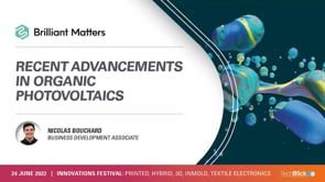
New HTL materials enable bridging the gap between the latest lab-level and production-level printed OPV performance: In this concise 5-min presentation, Nicolas Bouchard first shows the historical rise of OPV efficiencies from 2.5% in 2000 to >18% now, showing how evolution in materials has driven this rise (P3HT: PCBM --> emergence of push-pull polymers (PPP) --> rise of non-fullerene acceptors (NFAs)---> novel PPP and NFA). He then reveals the large gap between the best lab results and the best production level results with the highest industry-scale results being <8% !! One key factor holding back the efficiency of production-level OPVs is the unavailablity of a hole transport layer (HTL) compatible with the latest OPV donor and acceptor materials. This is because the latest novel donor and acceptor materials have wider bandgaps, thereby creating a large energy barrier with the common traditional HTL materials: PEDOT. This acts against charge injection and lowers efficiency. Thus, to get the best from the latest PPPs and NFAs in industry-scale processes, one requires an HTL material in a non halogenated solvent with a deep work function which can be printed in ambient conditions and which yields uniform thick (>100nm) layers. Brilliant Matters has developed such a material. Here, it is shown how this novel printable deep HTL achieves results equivalent to MoO3 (best evaporated material) when used with PTQ10 and NFA. This is an important step in further development and industrialization of organic photovoltaics to learn more about this technology and hear the latest from Brilliant Matters, please join us onsite in Eindhovne (the Netherlands) on 12-13 OCT 2022 https://www.techblick.com/electronicsreshaped #opv #photovotailc #printedelectronics #HTL #organicelectronics #organicsemiconductor #printedsolarcells #solarcells