
top of page


1/6


29 August 2025
Scalable Metal Oxide Nano Inks for High-Performance Organic, Perovskite, and Thin Film Photovoltaics and OLEDs
#PerovskiteSolarCells #OLED #OrganicPV #PrintedElectronics #NanoInks #ElectronTransportLayer #FlexibleElectronics #Optoelectronics #RollToRoll #SmartMaterials #EnergyTech #SolarInnovation #DisplayTechnology #NextGenMaterials #SustainableElectronics
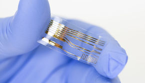
Author: Maryam Bari & Ashwani Jain PINA CREATION Unlocking printable, low-temperature charge transport layers for next-generation optoelectronics As next-generation optoelectronic technologies—such as Perovskite solar cells (PSCs), OLED displays, and Organic photovoltaics (OPVs) —move from lab to large-scale manufacturing, the pressure is on to find materials that are not only high-performing, but scalable, stable, and compatible with printed device architectures . A critical bottleneck remains the Electron Transport Layer (ETL) and Hole Transport Layer (HTL) . For technologies relying on delicate or flexible substrates, traditional materials such as Organic Semiconductors and traditional metal oxide inks pose serious limitations. High-temperature processing, moisture sensitivity, high cost, and limited lifetime all threaten the viability of commercial deployment. At PINA Creation , we’ve developed a line of ready-to-use SnO₂, NiO and ZnO nano inks that overcome these barriers and unlock practical, large-area fabrication for flexible and rigid optoelectronics. We are Exhibiting in Berlin. Visit our booth at the TechBlick Perovskite Connect event co-located with the Future of Electronics RESHAPED on 22-23 Oc...

28 August 2025
Introducing the full Perovskite Connect 2025 conference program
Perovskite Connect conference and exhibition | 22 & 23 OCT 2025, ECC, Berlin | Co-located with the Future of Electronics RESHAPED Berlin 2025 Perovskite Connect 2025 is shaping up to be the must-attend event for the perovskite industry , bringing together leading innovators, researchers, and manufacturers from across the globe. Taking place on 22–23 October 2025 at the ECC in Berlin , this specialist conference will run alongside the flagship Future of Electronics RESHAPED show. This article highlights some of the key talks that will take place during this conference. Explore the Full Agenda and Register before 12 September 2025 for the best rates Oxford PV – Edward Crossland presents the world’s first commercial perovskite-silicon tandem module . Breaking silicon’s efficiency limits, tandem technology delivers higher performance with minimal changes to existing production lines. The talk highlights Oxford PV’s milestone 2024 shipment, recent advances, and solutions for durability, scalability, and environmental compliance, demonstrating readiness for large-scale deployment. Hangzhou Microquanta Semiconductor – Yang Chen discusses the commercial readiness of perovskite PV . Drawing on lessons from industrial validation and field deployment, the talk addresses solutions to challenges in stability, efficiency, and scalable manufacturing. Insights into certification and real-world testing show how perovskite PV is evolving into a commercially viable alternative to s...

22 August 2025
Introducing the Program - Material, Ink and Paste Innovations
Why Should You Join TechBlick's The Future of Electronics RESHAPED? The Future of Electronics RESHAPED conference and exhibition (22 & 23 OCT 2025, Berlin) is set to be the most important event of the year focused on additive, hybrid, 3D, sustainable, wearable, soft and textile electronics.
This year the program features a world-class agenda with over over 100 superb invited talks from around the world, 12 industry- or expert-led masterclasses, 4 tours, and over 90 onsite exhibitors. In this article, we discuss and highlight various innovative talks at the event around the theme of Material, Ink and Paste Innovations.
In future articles, we will cover further technologies including smart surfaces, sustainable electronics, printed medical electronics, novel materials and beyond.
Explore the full agenda now and join the global industry in Berlin on 22 & 23 OCT 2025. Let us RESHAPE the Future of Electronics together, making it Additive, Hybrid, 3D, R2R, Soft, Flexible, Wearable, Textile and Sustainable. Heraeus Electronics – Ryan Banfield presents bridging additive and subtractive technologies through solderable polymer thick films. The talk highlights advances in polymer thick-film conductors that overcome long-standing barriers of poor solderability and thermal stability. This breakthrough enables flexible, low-cost circuits while reducing reliance on environmentally intensive subtractive manufacturing processes.
Blackleaf – Michael Friess presents graphe...
19 August 2025
Introducing the Program - Additive, Hybrid and 3D Electronics - Why Should You Join TechBlick's The Future of Electronics RESHAPED?
The flagship Future of Electronics RESHAPED conference and exhibition (22 & 23 OCT 2025, Berlin) is set to be the most important event of the year focused on additive, hybrid, 3D, sustainable, wearable, soft and textile electronics. This year the program features a world-class agenda with over over 100 superb invited talks from around the world, 12 industry- or expert-led masterclasses, 4 tours, and over 90 onsite exhibitors. In this article, we discuss and highlight various innovative talks at the event around the theme of Additive, Hybrid and 3D Electronics. In future articles, we will cover further technologies including smart surfaces, sustainable electronics, printed medical electronics, novel materials and beyond. Explore the full agenda now and join the global industry in Berlin on 22 & 23 OCT 2025. Let us RESHAPE the Future of Electronics together, making it Additive, Hybrid, 3D, R2R, Soft, Flexible, Wearable, Textile and Sustainable. Register before 12 Sept 2025 for the best rates Lockheed Martin (USA)– Paul Gaylo explores the transition of flexible hybrid electronics (FHE) from lab to field applications . Case studies on copper printing and flexible RF circuits illustrate how FHE can deliver SWaP-C advantages in defense systems while meeting reliability demands. The talk emphasizes concurrent engineering and early integration of design with advanced manufacturing to overcome barriers to FHE adoption. Fuji Corporation (Japan) – Ryojiro Tominaga demonstrates ad...

29 August 2025
Next Generation Conductive Ink
Authors: Alan Brown , Dr. Jay R Dorfman , Zac Hudson , Brandon Peters Contact: abrown@nagasechemtex.com , Nagase ChemteX America, LLC In the rapidly evolving field of Printed Electronics, the demand for robust, durable, and highly stretchable conductive inks is paramount for advancing applications in wearable technology and hybrid electronics. While existing conductive inks offer some degree of stretchability, they often exhibit a trade-off between mechanical resilience and electrical performance, leading to a significant increase in resistivity under strain. This limitation poses a critical challenge for engineers designing products that require consistent electrical conductivity across a wide range of motion. Nagase ChemteX America, LLC. (NCU) has developed a next-generation conductive ink, CI-1096, that is formulated to address this gap by providing superior stretchability while maintaining excellent and stable electrical resistivity. Our work constitutes a novel material solution that enables the development of more reliable and versatile stretchable electronic devices, paving the way for future innovations in biomedical sensors, smart textiles, and flexible displays. Stretch Ink Wearable Electrode NCU began this project with the goals of developing a Ag ink with increased stretchability, superior durability and high conductivity compared to CI-1036, an NCU Ag ink that has been on the market >10 years. This paper will document some of the challenges incurred during de...
26 August 2025
Introducing the Program - Additive and 3D Electronics Manufacturing Process Innovation
Why Should You Join TechBlick's The Future of Electronics RESHAPED? The Future of Electronics RESHAPED conference and exhibition (22 & 23 OCT 2025, Berlin) is set to be the most important event of the year focused on additive, hybrid, 3D, sustainable, wearable, soft and textile electronics. This year the program features a world-class agenda with over 100 superb invited talks from around the world, 12 industry- or expert-led masterclasses, 4 tours, and over 90 onsite exhibitors. In this article, we discuss and highlight various innovative talks at the event around the theme of Additive and 3D Electronics Manufacturing Process Innovation. In future articles, we will cover further technologies including smart surfaces, sustainable electronics, printed medical electronics, novel materials and beyond. In previous articles we introduced other innovations in Additive and 3D electronics (see here ) and also key material related innovations which will be showcased at the show (see here ) Explore the full agenda now and join the global industry in Berlin on 22 & 23 OCT 2025. Let us RESHAPE the Future of Electronics together, making it Additive, Hybrid, 3D, R2R, Soft, Flexible, Wearable, Textile and Sustainable. Explore the Full Agenda and Register before 12 September 2025 for the best rates GE Aerospace – Felippe Pavinatto presents additive electronics for aerospace applications in harsh environments . Examples include direct-write 3D printed passive RF sensors operating up...

20 August 2025
BrightSpot Automation | Customized defect imaging solutions for Perovskite and Tandem cell/panel architectures
#PerovskiteSolarCells #TandemSolar #Photovoltaics #SolarInnovation #DefectImaging #Electroluminescence #Photoluminescence #UVFluorescence #PVManufacturing #QualityControl #SolarTech #RenewableEnergy Author: Andrew Gabor, BrightSpot Automation LLC, gabor@brightspotautomation.com Perovskite PV technology faces severe challenges in scaling to the GW deployment level in terms of panel stability, conversion efficiency, and manufacturing yields. To help solve these challenges, BrightSpot Automation serves the entire Perovskite PV value chain with a suite of metrology tools implemented from R&D to product development to manufacturing to field testing. Our systems help identify defects, improve quality, reduce investment risk, and extend the performance of PV technology throughout its lifecycle. BrightSpot supplies customized Photoluminescence (PL) and Electroluminescence (EL) imaging tools which assess device spatial uniformity and resolve defects such as pinholes between the Perovskite film and carrier transport layers. Such pinholes may cause shunts that reduce fill factor and increase sensitivity to reverse bias damage. BrightSpot also supplies UV Fluorescence (UVF) tools which reveal the effects of moisture ingress due to incomplete sealing. The table above shows which of these tools are applicable at different stages during manufacturing, accelerated testing, and field exposure. EL involves injecting current into the device with a power supply such that the device glows ...

19 August 2025
Revolutionizing High-Volume Production: The Intlvac Icarus Indium Solder Bump Deposition System
In the fast-paced world of advanced manufacturing, precision, speed, and reliability are non-negotiable. Enter the Intlvac Icarus Indium Solder Bump Deposition System—a game-changing solution designed to meet the rigorous demands of high-volume production. With over 30 years of expertise in system manufacturing and coating services, Intlvac has engineered a system that delivers exceptional performance, minimal maintenance, and rapid turnaround times. A solder bump is a small, raised deposit of indium solder that is typically applied to the surface of a microelectronic device. Solder bumps are commonly used in semiconductor packaging and flip-chip bonding processes, microprocessors, integrated circuits, and other electronic components. They provide an efficient and reliable method for connecting chips to substrates, allowing for high-performance and compact devices. We are Exhibiting! Visit our booth at the MicroLED Connect & AR/VR Connect in Eindhoven on 24-25 September 2025 Why Indium Bumps? Indium bumps are essential for advanced applications due to their unique properties. They enable higher packing density and increased device speeds, making them ideal for flip-chip bonding in pixel readout applications. Additionally, indium offers strong mechanical properties and superconductivity at temperatures below 3.4K, ensuring reliable performance in demanding environments. Its role as an under-bump diffusion barrier further enhances device performance by preventing material int...
bottom of page